Note : Les descriptions sont présentées dans la langue officielle dans laquelle elles ont été soumises.
CA 02752277 2011-09-12
R-9229
PHOTOVOLTAIC MODULES
Gregory F. Jacobs
BACKGROUND
Field of the Disclosure
[0001] The following is directed to photovoltaic modules, and more
particularly
substrates for use with certain photovoltaic modules.
Description of the Related Art
[00021 Alternative energy sources continue to be in greater demand to stem our
reliance
upon fossil fuels, since fossil fuels are proven to be in limited supply and
difficult to find,
1o store, and distribute. Additionally, fossil fuels are becoming more
expensive due to
increasing scarcity and political issues surrounding the limited supply. It is
also worth
noting that fossils fuels have been shown to have negative effects on the
global
environment, including for example, air pollution and reduction of the ozone
layer.
[0003] As such, the global community has a growing interest in harvesting
energy from
other natural resources, such as wind, water, and solar energy. In particular
reference to
solar energy, "photovoltaic cells" are typically used to convert solar energy
into electrical
energy. Conventional photovoltaic cells can be made of semiconductor
materials, which
aid the conversion of solar energy to electrical energy that can be
distributed for common
uses. Various photovoltaic cells have been integrated into solar farms (e.g.,
in the desert
regions of the Southwestern United States), as well as integrated into
conventional
residences and office buildings. See, for example, US Patents 5,437,735,
5,575,861,
6,875,914, 6,883,290, 6,928,775. However, given the variety of uses, the
photovoltaic
cells are being exposed to ever greater variety of environments.
[0004] There is a continuing need for photovoltaic modules having capabilities
to be
deployed into a variety of environments, while maintaining sufficient
efficiency in power
generation.
-1-
CA 02752277 2011-09-12
R-9229
SUMMARY
[0005] According to a first aspect, a photovoltaic module includes a
photovoltaic element
and a substrate coupled to the photovoltaic element. The substrate can be made
of an
amorphous phase material and have a compression region abutting an external
surface of
the substrate, wherein the compression region extends for an average depth
into the
substrate of at least about 50 microns.
[0005] In another aspect, a photovoltaic module includes a photovoltaic
element and a
substrate coupled to the photovoltaic element made of an amorphous phase
material. The
substrate includes a compression region abutting an external surface of the
substrate and
to comprises a compressive stress of at least about 200 MPa.
[0007] In yet another aspect, a photovoltaic module includes a photovoltaic
element and a
substrate coupled to the photovoltaic element, wherein the substrate comprises
a Young's
Modulus of at least about 40 GPa and a fracture toughness of at least about
0.4 MPa m,2.
[0008] In still another aspect, a photovoltaic module includes a photovoltaic
element and
a first substrate coupled to the photovoltaic element comprising an inorganic,
amorphous
phase material, wherein the first substrate has an average thickness of not
greater than
about 3.0 mm.
[0009] According to another aspect, a roofing element includes a photovoltaic
element, a
substrate coupled to the photovoltaic element, wherein the substrate comprises
an
amorphous phase, wherein the substrate has a surface region under a
compressive stress
of at least about 200 MPa. The roofing element can further include a
decorative overlay
overlying the photovoltaic element, wherein the decorative overlay simulates
the
appearance of conventional building materials and is substantially transparent
to radiation
within an operating wavelength range of the photovoltaic element.
[0010] In yet another aspect, a photovoltaic module includes a photovoltaic
element and a
first substrate coupled to the photovoltaic element comprising an inorganic,
amorphous
phase material. The first substrate has an average thickness of not greater
than about 3.0
mm and a fracture toughness of at least about 0.4 MPa ml/2.
[oot t] According to one aspect, a roofing element has a body including a
photovoltaic
module and an attachment mechanism configured to attach the body to a surface
of a
-2-
CA 02752277 2011-09-12
R-9229
building structure. The photovoltaic module includes a substrate comprising an
amorphous phase material having a compression region abutting an external
surface of
the substrate, wherein the compression region extends for an average depth
into the
substrate of at least about 50 microns.
[0012] In still another aspect, a building element includes a body of a
building material
configured to be attached to a structure, and a photovoltaic module attached
to the body
via an attachment mechanism. The photovoltaic module includes a substrate
comprising
an amorphous phase material having a compression region abutting an external
surface of
the substrate, wherein the compression region extends for an average depth
into the
substrate of at least about 50 microns.
BRIEF DESCRIPTION OF THE DRAWINGS
[0013] The present disclosure may be better understood, and its numerous
features and
advantages made apparent to those skilled in the art by referencing the
accompanying
drawings.
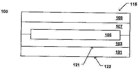
[0014] FIG. I includes a cross-sectional diagram of a photovoltaic module
according to an
embodiment.
[0015] FIG. 2 includes a cross-sectional diagram of a photovoltaic module
according to
an embodiment.
[0016] FIG. 3 includes a cross-sectional diagram of a photovoltaic module
according to
an embodiment.
[0017] FIG. 4 includes a cross-sectional diagram of a photovoltaic module
according to
an embodiment.
[0018] FIG 5 includes a cross-sectional diagram of a photovoltaic module
according to an
embodiment.
[oo19] FIG. 6 includes a cross-sectional diagram of a photovoltaic module
according to
an embodiment.
[0020] FIG. 7 includes a cross-sectional diagram of a photovoltaic module
according to
an embodiment.
-3-
CA 02752277 2011-09-12
R-9229
[0021] FIG. 8 includes an illustration of a body in the form of a roofing
element
incorporating a photovoltaic module in accordance with an embodiment
[0022] The use of the same reference symbols in different drawings indicates
similar or
identical items.
DETAILED DESCRIPTION
[0023] The following is directed to photovoltaic modules. As used herein, the
term
"photovoltaic module" means one or more photovoltaic cells electrically
connected to
operate as an integral unit. "Infrared radiation" means electromagnetic
radiation having a
wavelength of from 1.4 micrometers to 1000 micrometers. "Near infrared
radiation"
to means electromagnetic radiation having a wavelength of from 0.75
micrometers to 1.4
micrometers. "Visible radiation" means electromagnetic radiation having a
wavelength of
from 350 to 750 nanometers. "Substantially transmissive" when referring to
radiation
means having an average transmission coefficient of at least 50 percent.
[0024] FIG. I includes a cross-sectional diagram of a photovoltaic module
according to
an embodiment. As illustrated, the photovoltaic module 100 can include a
photovoltaic
element 105, which can include one or more semiconducting layers (not shown)
for
converting solar energy to electricity. The photovoltaic element 105 can
include
semiconductor single crystal silicon layers, non-single crystal semiconductor
silicon
layers such as amorphous semiconductor silicon layers, microcrystalline
semiconductor
silicon layers, nanocrystalline semiconductor silicon layers, polycrystalline
semiconductor silicon layers, and compound semiconductor layers. Photoactive
semiconductor silicon layers can be stacked, and the junctions between the
stacked layers
can be of the pn-type, the np-type, the Schottky type, etc. Photoactive layers
can include
n-type silicon layer doped with an electron donor such as phosphorous,
oriented towards
incident solar radiation, and a p-type silicon layer doped with an electron
acceptor, such
as boron. Semiconductor stacks can include transparent electrical current
conducting
layers formed from electrically conductive semiconductor materials such as
indium oxide,
stannic oxide, zinc oxide, titanium dioxide, cadmium stannate, and the like.
The
photovoltaic element 105 can further include a backing plate and current
collecting
electrodes, which are not illustrated.
-4-
CA 02752277 2011-09-12
R-9229
[0025] The photovoltaic element 105 can include one or more interconnected
photovoltaic cells. The photovoltaic cells of the photovoltaic element can be
based on
any desirable photovoltaic material system, such as monocrystalline silicon;
polycrystalline silicon; amorphous silicon; III-V materials such as indium
gallium nitride;
II-VI materials such as cadmium telluride; and more complex chalcogenides
(group VI)
and pnicogenides (group V) such as copper indium diselenide or CIGS. For
example, one
type of suitable photovoltaic cell includes an n-type silicon layer (doped
with an electron
donor such as phosphorus) oriented toward incident solar radiation on top of a
p-type
silicon layer (doped with an electron acceptor, such as boron), sandwiched
between a pair
of electrically-conductive electrode layers. Another type of suitable
photovoltaic cell is
an indium phosphide-based thermo-photovoltaic cell, which has high energy
conversion
efficiency in the near-infrared region of the solar spectrum. Thin film
photovoltaic
materials and flexible photovoltaic materials can be used in the construction
of
encapsulated photovoltaic elements for use in the present invention. In one
embodiment
of the invention, the photovoltaic element includes a monocrystalline silicon
photovoltaic
cell or a polycrystalline silicon photovoltaic cell.
[0026] The photovoltaic element 105 can be disposed between a lower
encapsulant layer
103 and an upper encapsulant layer 107. The encapsulant layers 103 and 107 can
be
formed around the photovoltaic element 105 to protect the delicate components
of the
photovoltaic element 105 and provide structure for affixing other components
of the
photovoltaic module 100. Certain suitable properties of the encapsulant layers
103 and
107 include impact resistance, low temperature resistance, high temperature
resistance,
environmental stability, and adhesion for use in encapsulating the
photovoltaic element
103 in photovoltaic modules 100 for exterior use.
[0027] The lower and upper encapsulant layers 103 and 107 can include an
organic
material. Suitable organic materials can include polymers, such as polyamids,
polyimides, resins, epoxies, and a combination thereof. According to one
particular
embodiment, the lower and upper encapsulant layers 103 and 107 consist
essentially of a
resin, and further may be formed of the same resin material. Generally, the
upper
encapsulant layer 107 can include a material that is substantially transparent
or
transmissive to both near infrared radiation and infrared radiation, such as
for example, an
ethylene vinyl acetate resin.
-5-
CA 02752277 2011-09-12
R-9229
[0028] Organic materials suitable for use in the upper and lower encapsulant
layers 103
and 107 can include resins, such as ethylene vinyl acetate copolymer resins,
ethylene
ethyl acrylate copolymer resins, ethylene methyl acrylate copolymer resins,
polyvinyl
butyral resins, polyurethane resins, fluororesins, and silicone resins. It
will be appreciated
that resins, which are substantially transparent or at least transmissive
radiation within the
operating wavelength range (e.g., near infrared radiation and to infrared
radiation), such
as ethylene vinyl acetate resins, are suitable. The resins can be employed in
the form
thermoplastic or thermosetting fluids applied to a substrate including the
photovoltaic
materials, as films applied to the photovoltaic materials, or the like.
Physical properties
of some resins can be altered by utilizing particular average molecular
weight, molecular
weight distributions, degrees of branching, and levels of crosslinking.
[0029] In one particular embodiment, the encapsulant layers 103 and 107 can
include
certain amounts, such as between about 0.1 to 1.0 percent by weight of the
resin, of
additives to enhance the ultraviolet radiation resistance and/or the radiation
stabilization
of the encapsulant resin. For example, ultraviolet radiation absorbers such as
benzophenones, benzotriazoles, cyanoacrylates, and salicylic acid derivatives
can be
employed, including 2-hydroxy- 4-methoxybenzophenone, 2-hydroxy-4-n-
octyloxybenzophenone, 2-(2-hydroxy-5-t- octylphenyl)benzotriazole, titanium
dioxide,
cerium (IV) oxide, zinc oxide and stannic oxide. Ultraviolet radiation
absorbers can
include nanoparticle zinc oxides and titanium dioxides. Suitable radiation
stabilizers,
which can be used in conjunction with ultraviolet radiation absorbents,
include hindered
amine bases such as, for example, derivatives of 2,2,6,6-tetramethyl
piperidine of lower
molecular weight or in polymeric form. The encapsulant layers 103 and 107 can
also
include anti-oxidants such as hindered phenols, and adhesion-promoting agents
such as
organic titanates, organic zirconates, organosilanes, and a combination
thereof.
[0030] A substrate 101 can be coupled to the photovoltaic element 105, and
particularly,
can be bonded directly to the lower encapsulant layer 103, such that the
substrate 101
underlies the photovoltaic element 105 and provides suitable support for the
photovoltaic
module 100. The substrate 101 can include a rigid material, which can be
transparent or
transmissive to radiation within the range of operating wavelengths of the
photovoltaic
element. As will be appreciated, the photovoltaic element 105 can have a range
of
operating wavelengths, and different photovoltaic elements have different
power
-6-
CA 02752277 2011-09-12
R-9229
generation efficiencies with respect to different parts of the solar spectrum.
For example,
amorphous doped silicon is most efficient at visible wavelengths, and
polycrystalline
doped silicon and monocrystalline doped silicon are most efficient at near-
infrared
wavelengths. Solar radiation includes light of wavelengths spanning the near
UV, the
visible, and the near infrared spectra. As used herein, when the term "solar
radiation" or
"solar energy" refer to wavelengths of radiation ranging from 300 nm to 1500
nm. As
used herein, the range of operating wavelengths for a given photovoltaic
element is the
wavelength range over which the relative spectral response is at least 10% of
the maximal
spectral response. According to certain embodiments of the invention, the
operating
wavelength range of the photovoltaic element 105 is within a range between
about 300
nm and about 2000 nm, and more particularly within a range between about 300
nm and
about 1200 nm.
[0031] According to one embodiment, the substrate 101 can include an inorganic
material, such as a metal, metal alloy, ceramic, glass, and a combination
thereof.
Particular photovoltaic modules can have substrates 101 made of glass, and can
consist
essentially of glass. Certain suitable glasses can include aluminosilicate
glass materials,
and more particularly, an alkali-aluminosilicate material. According to one
embodiment,
the substrate 101 can be an alkali-aluminosilicate material containing a
majority amount
(on a mol% basis) of silica (Si02). For example, the amount of silica can be
within a
range between about 55 mol% and about 75 mol%, and more particularly within a
range
between about 60 mol% and about 70 mol%.
[0032] In certain instances, the substrate 101 can include a particular amount
of alumina
(A1203), such as between about 5 mol% and about 15 mol%. Some substrate 101
materials can include an amount of alumina (A1203) within a range between
about 6
mol% and about 14 mol%, and more particularly, between about 8 mol% and about
12
mol%.
[0033] Moreover, the substrate 101 may include some content of boron oxide
(B203).
For example, boron oxide can be present within the substrate 101 within a
range between
about 0 mol% and about 15 mol%, such as between about 0 mol% and about 8 mol%,
and
more particularly, within a range between about 0.5 mol% and about 5 mol%.
-7-
CA 02752277 2011-09-12
R-9229
[0034] Certain substrate 101 materials may incorporate a certain amount of
lithium oxide
(Li2O). According to one embodiment, the substrate 101 can have an amount of
lithium
oxide within a range between about 0 mol% and about 20 mol%, such as between
about 0
mol% and about 10 mol%, or even between about 0.5 mol% and about 5 mol%.
Still,
certain substrate compositions can be essentially free of lithium oxide
(Li2O). As used
herein, "essentially free of lithium" means that lithium is not intentionally
added to the
raw materials during any of the processing steps leading to the formation of
the alkali
aluminosilicate glass.
[0035] In addition to the compositions noted above, the substrate 101 can have
particular
amount of potassium oxide (K2O). For example, certain suitable contents of
potassium
oxide can be within a range between about 0 mol% and about 8 mol%, within a
range
between about I mol% and about 6 mol%, and even within a range between about 2
mol% and about 5 mol%.
[0036] The substrate 101 can include an amount of sodium oxide (Na2O) within a
range
between about 0 mol% and about 20 mol%. Other substrate compositions contain
an
amount of sodium oxide within a range between about 5 mol% and about 18 mol%,
or
even within a range between about 12 mol% and about 16 mol%.
[00371 Notably, the substrate 101 can be made of a material having a
composition
wherein the total content of alkali oxide compounds (e.g., lithium oxide
(Li2O), sodium
oxide (Na2O), and potassium oxide (K2O)) is particularly limited. For example,
the
substrate 101 can have a total content of alkali oxide compounds within a
range between
about 5 mol% and about 20 mol%, and even within a range between about 12 mol%
and
about 20 mol%.
[0038] The substrate 101 can be formed of a material containing particular
amounts of
magnesium oxide (MgO). That is, certain substrates 101 are formed to have an
amount of
magnesium oxide within a range between about 0 mol% and about 10 mol%, such as
between about 2 mol% and about 8 mol%, or even between about 4 mol% and about
6
mol%.
[0039] Likewise, the substrate 101 can be a material having a certain content
of calcium
oxide (CaO). Particularly suitable amounts of calcium oxide can be within a
range
-8-
CA 02752277 2011-09-12
R-9229
between about 0 mol% and about 10 mol%, such as between about 0 mol% and about
8
mot%, and even within a range between about 0.2 mol% and about 5 mol%.
[00401 Certain substrate 101 compositions may also contain a limited amount of
strontium oxide (SrO). The amount of strontium oxide within the substrate 101
can be
within a range between about 0 mol% and about 5 mol%.
[0041] The total content of alkaline earth oxide compounds (i.e., magnesium
oxide
(MgO), calcium oxide (CaO), and strontium oxide (SrO) present within the
substrate 101
can be within a range between about 0 mot% and about 10 mol%. For certain
embodiments, the total amount of alkaline earth oxides can be within a range
between
about 2 mol% and about 10 mol% or even within a range between about 5 mol% and
about 8 mol%.
[0042] Some substrate 101 compositions can include a minor amount of tin oxide
(Sn02).
According to one embodiment, the substrate 101 can be formed to have an amount
of tin
oxide within a range between about 0 mol% and about 5 mol%, such as within a
range
between about 0 mol% and about 2 mol%, and even more particularly within a
range
between about 0.5 mol% and about 2 mol%.
[0043] An amount of cerium oxide (CeO2) can be present within the material of
the
substrate 101. For example, certain substrates 101 can contain an amount of
cerium oxide
within a range between about 0 mol% and about 5 mol%, such as between about 0
mol%
and about 2 mol%, and even between about 0.5 mol% and about 2.0 mol%.
[0044] According to another embodiment, the substrate 101 can be formed of a
particularly thin sheet of glass. That is, for example, the substrate 10 1 can
have a total
average thickness, measured as a distance between the surfaces 121 and 122, of
not
greater than about 3mm. In particular instances, the substrate 101 can be
thinner, having
a total average thickness of not greater than about 2.8 mm, such as not
greater than about
2.5 mm, not greater than about 2.2 mm, or even not greater than about 2.0 mm.
Still, the
substrate 101 can have a total average thickness within a range between about
0.5 mm
and about 3.0 mm, such as between about 0.5 mm and about 2.8 mm, or even
between
about 0.5 mm and about 2.5 mm.
-9-
CA 02752277 2011-09-12
R-9229
[00451 Notably, the substrate 101 can be a glass material formed through a
fusion-draw
process. That is, the glass is capable of being formed into sheets using
fusion-draw
methods. The fusion-draw process uses a drawing tank that has a channel for
accepting
molten glass raw material. The channel has weirs that are open at the top
along the length
of the channel on both sides of the channel, and when the channel fills with
molten
material, the molten glass overflows the weirs. Due to gravity, the molten
glass flows
down the outside surfaces of the drawing tank. These outside surfaces extend
down and
inwardly so that they join at an edge below the drawing tank. The two flowing
glass
surfaces join at this edge to fuse and form a single flowing sheet. The fusion
draw method
offers the advantage that, since the two glass films flowing over the channel
fuse together,
neither outside surface of the resulting glass sheet comes in contact with any
part of the
apparatus. Thus, the surface properties are not affected by such contact.
[0046] Notably, the glass forming the substrate 101 material can have a high
liquidus
viscosity for suitable forming using the fusion-draw process. For example, the
glass
material of the substrate can have a liquidus viscosity of at least 230
kilopoise (kpoise)
and, in other embodiments, the liquidus viscosity is at least 250 kpoise.
[00471 In one embodiment, the substrate 101 can be a glass material that is
strengthened
by ion-exchange. As used herein, the term "ion-exchanged" is understood to
mean that
the glass is strengthened by ion exchange processes that are known to those
skilled in the
glass fabrication arts. Such ion exchange processes include, but are not
limited to,
treating the heated glass with a heated solution containing ions having a
larger ionic
radius than ions that are present in the glass surface, thus replacing the
smaller ions with
the larger ions. Potassium ions, for example, can replace sodium ions in the
glass.
Alternatively, other alkali metal ions having larger atomic radii, such as
rubidium or
cesium can replace smaller alkali metal ions in the glass. Similarly, other
alkali metal
salts such as, but not limited to, sulfates, halides, and the like may be used
in the ion
exchange process. In one embodiment, the glass can be chemically strengthened
by
placing it a molten salt bath comprising NaNO3 or KNO3 for a predetermined
time period
to achieve ion exchange. In one embodiment, the temperature of the molten salt
bath can
be about 430 C, and the glass can stay in the salt bath for a duration of
approximately
eight hours. It will be appreciated that multiple and successive ion exchange
processes
-10-
CA 02752277 2011-09-12
R-9229
can be undertaken. For example, a first ion-exchange process can be completed
and a
second ion-exchange process can be completed after the first ion-exchange
process.
[0048] Due to the ion exchange process, the substrate 101 can have a dopant
material
(i.e., an ion or element of the salt that has been exchanged within the glass
material) that
is present in a higher concentration within the compression region than a
region within
the substrate 101 outside of the compression region. In certain instances, the
dopant
material can include an alkali element, and particularly sodium.
[0049] The ion exchange process facilitates the formation of a compression
region within
the glass substrate 101, wherein the compression region is abutting an
external surface
to (i.e., surface 121 or 122) of the substrate 101 and extends for a
particular depth into the
body of the substrate 101. For example, the compression region can extend for
an
average depth of at least about 50 microns. In other embodiments, the depth of
the
compression region is at least about 60 microns, such as at least about 70
microns, at least
about 80 microns, at least about 90 microns, or even at least about 100
microns. Still, the
depth of the compression region can be limited, for example, the compression
region may
not extend for a depth of greater than about 300 microns, such as not greater
than about
250 microns, or even not greater than about 210 microns. Particular glass
substrates 101
can have a compression region that has an average depth within a range between
about 50
microns and about 200 microns, such as between about 70 microns and about 200
microns, or even between about 70 microns and about 150 microns.
[00501 Moreover, the formation of a compression region results in a
compressive stress
within the compression region, measureable at the surface of the glass. The
compressive
stress within the glass substrate 101 can be at least about 200 MPa. In other
instances, the
compressive stress can be greater, such as at least about 300 MPa, at least
about 400 MPa,
at least about 500 MPa, at least about 600 MPa, at least about 700 MPa, or
even at least
about 800 MPa. Particular glass substrates 101 can be formed to have a
compressive
stress within the compression region between about 200 MPa and about 1000 MPa,
or
even between about 400 MPa and about 1000 MPa.
[0051] Formation of the compression region near the external surface of the
substrate 101
can induce a tensile stress in a central region of the substrate. According to
one
embodiment, the substrate 101 can have a tension of at least about 2 MPa=cm
within the
-11-
CA 02752277 2011-09-12
R-9229
central region. In other embodiments, the tension can be greater, such as at
least about
2.5 MPa=cm, at least about 2.8 MPa=cm, or even at least about 3 MPa-cm.
Particular
substrates 101 can have a central region having a tension within a range
between about 2
MPa-cm and about 4 MPa=cm, or more particularly within a range between about
2.5
MPa=cm up to about 3.8 MPa=cm
[0052] Based on the use of the fusion-draw process coupled with the ion-
exchange
process, glass substrates of the embodiments herein can have improved
geometric
properties over other glasses, such as those formed through a float process.
For example,
the glass substrate 101 can have a warpage of less than about 0.5 mm for a 300
mm x 400
to mm sheet. In another embodiment, the warpage is less than about 0.3 mm.
[0053] The substrate 101 can include a glass material having particular
mechanical,
chemical, and physical properties. For example, the substrate 101 can include
a glass
having a softening point (1076 poises) of not greater than about 865 C. In
still other
instances, the substrate 101 can include a glass material having a softening
point of not
greater than about 855 C, not greater than about 850 C or even not greater
than about
845 C. Particular glass materials for use in the substrate 101 can have a
softening point
within a range between about 830 C and about 865 C, and more particularly
within a
range between about 835 C and 850 C.
[0054] Additionally, the substrate 101 can include a glass having a strain
point (1014.7
poises) of not greater than about 590 C. In still other instances, the
substrate 101 can
include a glass material having a strain point of not greater than about 580
C, such as not
greater than about 570 C. Particular glass materials for use in the substrate
101 can have
a strain point (10147 poises) within a range between about 530 C and about 590
C, and
more particularly, within a range between about 540 C and about 570 C
[00551 Further properties of material suitable for use in the substrate 101
can include a
glass having an annealing point (1013.2 poises) of not greater than about 635
C. For
example, the glass material can have an annealing point of not greater than
about 625 C,
such as not greater than about 620 C, or even not greater than about 615 C.
Particular
glass materials for use in the substrate 101 can have an annealing point
within a range
3o between about 590 C and about 630 C, and more particularly, within a range
between
about 595 C and about 620 C.
-12-
CA 02752277 2011-09-12
R-9229
[00561 The substrate 101 can have a density within a range between about
between about
2.40 g/cm3 and about 2.50 g/cm3. In other embodiments, the density can be
within a
range between about 2.42 g/cm3 and about 2.46 g/cm3.
[0057] Another particular aspect of the material of the substrate 101 is that
it can be
particularly resilient to cracking and shattering. Such properties are
particularly
advantageous in the context of photovoltaic cells that are deployed in a
variety of
environments, and cracks within the substrate 101 (or other particular
components as
discussed herein) can present regions susceptible to chemical attack,
mechanical failure,
and operational flaws of the module. For example, the substrate 101 can
include a
material, such as a glass, having a Young's Modulus of at least about 40 GPa.
In other
instances, the substrate 101 can have a Young's Modulus of at least about 50
GPa, such
as at least about 55 GPa, at least about 60 GPa, or even at least about 65
GPa. Particular
substrates 101 can utilize a glass material having a Young's Modulus within a
range
between about 50 GPa and about 100 GPa, such as between about 60 GPa and about
90
GPa.
[00581 Certain substrates 101 can include a material having a fracture
toughness of at
least about 0.4 MPa m'12. In other instances, the substrate 101 can have a
fracture
toughness of at least about 0.5 MPa mv2, such as at least about 0.6 MPa m'12,
or even at
least about 0.65 MPa m1"2. According to an embodiment, the substrate 101 can
include a
material having a fracture toughness of not greater than about 0.9 MPa m'/2,
or even not
greater than about 0.8 MPa m1/2.
[00591 The chemical durability of the substrate 101 may be particularly
suitable for use in
photovoltaic applications. For example, the substrate 101 can include a
material, such as
a glass material, having a suitable chemical durability, which is measured as
a weight loss
of not greater than about 1 mg/cm2 when the substrate is exposed to a solution
of 5% HCI
for 24 hours at a temperature of 95 C. In fact, the chemical durability of
certain
substrates 101 can have a weight loss of not greater than about 0.8 mg/cm2,
not greater
than about 0.6 mg/cm2, not greater than about 0.4 mg/cm2, not greater than
about 0.2
mg/cm2, or even not greater than about 0.08 mg/cm2. In fact, the chemical
durability can
be within a range between about 0.01 mg/cm2 and about 1 mg/cm2, or even
between
about 0.01 mg/cm2 and 0.2 mg/cm2.
-13-
CA 02752277 2011-09-12
R-9229
[0060] While the foregoing has noted that certain substrates 101 can include a
glass
material having particular features, other materials can be used in the
substrate 101. For
example, other suitable glass materials include organic materials, ceramics,
metals, metal
alloys, composites, and combinations thereof. Moreover, an electrically
insulating
material is suitable for use in the substrate 101. Particularly suitable
organic materials
can include nylon, polytetrafluoroethylene, polycarbonate, polyethylene,
polystyrene,
polyester, or the like,
[0061] As further illustrated in FIG. 1, the photovoltaic module 100 can
further include a
substrate 109. The substrate 109 can be a superstrate or cover plate for the
photovoltaic
element 105. As illustrated, an external surface of the substrate 109 defines
the active
face 115 of the photovoltaic module, which is the surface designed to receive
the solar
radiation. The substrate 109 can have any and all of the features of the
substrate 101
described in the embodiments herein. Notably, the substrate 109 can be a glass
material,
and particularly an alkali-aluminosilicate material as described herein.
[0062] It will be appreciated, that in addition to the features described
herein, the
substrate 109 can have an antireflection coating can be applied to a surface,
such as the
external surface defining the active face 115, for radiation adsorption. The
antireflection
coating can contribute to a characteristic blue or black appearance of the
photovoltaic
module. Other contributing factors can include the semiconducting layers
within the
photovoltaic element, and other component layers within the module. It will
further be
appreciated, that since the substrate 109 defines the active face 115 of the
photovoltaic
module 100, the substrate 109 is preferably substantially transmissive to
solar radiation
within the range of operating wavelengths of the photovoltaic element 103.
[0063] Additionally, in certain embodiments herein, an optional infrared
transmissive
film (not illustrated) can be coupled to the exterior surface of the substrate
109 defining
the active face 115. The infrared transmissive overlay film can include a
surface coating
including pigment absorbing radiation in the visible range arranged in a
decorative
pattern.
[0064] FIG. 2 includes a cross-sectional diagram of a photovoltaic module
according to
3o an embodiment. As illustrated, the photovoltaic module 200 includes certain
same
features of the photovoltaic module 100 of FIG. 1. The photovoltaic module 200
includes
-14-
CA 02752277 2011-09-12
R-9229
a substrate 101, a lower encapsulant layer 103 overlying the substrate 101, an
upper
encapsulant layer 107 overlying the lower encapsulant layer 103, a
photovoltaic element
105 disposed between the upper and lower encapsulant layer 107 and 103, and a
substrate
109 overlying the photovoltaic element 105 and the upper encapsulant layer
107.
[0065] Additionally, the photovoltaic module 200 comprises an overlay layer
230
overlying the substrate 109. In particular, the overlay layer 230 can be
directly coupled to
the upper surface of the substrate 109. As such, the overlay layer 230 can
define the
active surface 115 of the photovoltaic module 200.
[0066] According to one particular embodiment, the overlay layer 230 can be a
decorative overlay. A decorative overlay can be formed to simulate the
appearance of
conventional building materials, particularly building materials against which
the
photovoltaic module is placed. Examples, of conventional building materials
include
roofing (e.g., shingles), siding, natural surfaces (e.g., stone, brick,
concrete, etc.), glass, or
metal surfaces.
[0067] Some decorative overlay layers can be formed to have a three-
dimensional
pattern, which may be created by embossing, molding, selectively coating, or
by any of
the many ways known in the art for creating a three-dimensional pattern. In
addition, the
overlay layer 230 can include a pigment configured to absorb radiation in the
visible
range, providing a hue simulating the hue of conventional building materials.
[0068] According to one embodiment, the overlay layer 230 can include an
infrared
transmissive film 111 overlying, and particularly in direct contact with the
substrate 109.
In one embodiment, the film I I l can be transmissive or transparent in the
near infrared
range and scatter, reflect or absorb light in the visible range of the
spectrum to produce a
particular appearance. Certain polymers suitable for use in the film 111 can
include
acrylics, polycarbonates, and fluoropolymers, such as fluororesins.
[0069] Additionally, the overlay layer 230 can include an infrared-
transmissive pigment
within the film 111 can be used to provide visible color to the coating or
film. Some
suitable infrared-transmissive pigments can be inorganic or organic. In the
case of
organic pigments, it is preferred to include a protective overlay film that
contains an
ultraviolet absorber. The ultraviolet absorber provides an element of
weatherability
enhancement for organic transparent pigments. Examples of infrared-
transmissive
-15-
CA 02752277 2011-09-12
R-9229
pigments include zinc sulfide, zinc oxide, nanoparticle titanium dioxide and
other
nanopigments, Cl Pigment Black 3 1, Cl Pigment Black 32, Cl Pigment Red 122,
Cl
Pigment Yellow 13, perylene pigments, ultramarine blue pigments, quinacrodone
pigments, azo pigments, and pealescent pigments.
[0070] The overlay layer 230 can be formed using a deposition process,
lamination
process, printing process, spraying, and a combination thereof. The infrared
transmissive
overlay film 111 may be coupled to the surface of the substrate 109 by an
adhesive film
112 of infrared transmissive adhesive material. Still, in another embodiment,
the
adhesive film 112 may be omitted, and the overlay film 111 can secured
otherwise, such
by suitable fasteners or edging material (not shown).
[0071] FIG. 3 includes a cross-sectional diagram of a photovoltaic module
according to
an embodiment. As illustrated, the photovoltaic module 300 includes certain
same
features of the photovoltaic module 100 of FIG. 1. The photovoltaic module 100
includes
a substrate 101, a lower encapsulant layer 103 overlying the substrate 101, an
upper
encapsulant layer 107 overlying the lower encapsulant layer 103, a
photovoltaic element
105 disposed between the upper and lower encapsulant layer 107 and 103, and a
substrate
109 overlying the photovoltaic element 105 and the upper encapsulant layer
107.
[0072] Additionally, the photovoltaic module 300 comprises an overlay layer
330
underlying the substrate 109. In particular, the overlay layer 330 may be
directly coupled
to the upper surface of the upper encapsulant layer 107 and the lower surface
of the
substrate 109. In particular, an adhesive film (not shown) may be used to bond
the
overlay layer 330 to any of the adjacent layers (i.e., the upper encapsulant
layer 107 or the
substrate 109).
[0073] The substrate 109 can define the active surface 115 of the photovoltaic
module
300. The overlay layer 330 can have all the attributes of other overlay layers
described
herein in other embodiments.
[0074] While not particularly illustrated, it will be appreciated that in an
alternative
embodiment, the overlay layer 330 can be disposed in another position within
the
photovoltaic module. For example, the overlay layer 330 can be disposed within
the
upper encapsulant layer 107.
-16-
CA 02752277 2011-09-12
R-9229
[0075] FIG. 4 includes a cross-sectional diagram of a photovoltaic module
according to
an embodiment. As illustrated, the photovoltaic module 400 includes certain
same
features of the photovoltaic module 100 of FIG. 1. The photovoltaic module 400
includes
a substrate 101, a lower encapsulant layer 103 overlying the substrate 101, an
upper
encapsulant layer 107 overlying the lower encapsulant layer 103, a
photovoltaic element
105 disposed between the upper and lower encapsulant layer 107 and 103, and a
substrate
109 overlying the photovoltaic element 105 and the upper encapsulant layer
107.
[0076] Additionally, the photovoltaic module 400 comprises an overlay layer
430
overlying the substrate 109. In particular, the overlay layer 430 may be
directly coupled
1o to the upper surface of the substrate 109. In particular, an adhesive film
(not shown) may
be used to bond the overlay layer 430 to the substrate 109.
[0077] The overlay layer 430 can define the active surface 115 of the
photovoltaic
module 300. The overlay layer 330 can have all the attributes of other overlay
layers
described herein in other embodiments. As illustrated, the overlay layer 430
can be a
Is decorative overlay, which can have an appearance designed to simulate
conventional
building materials. The overlay layer 430 can have an irregularly shaped upper
surface to
simulate certain conventional building materials. For example, the overlay
layer 430 can
have protruding features (e.g., jagged edge or roughened surface) extending
from the
upper surface of the overlay layer 430 to simulate the appearance of
conventional
20 building materials. It will be appreciated that certain overlay layers can
be formed to
have a patterned surface.
[00781 FIG. 5 includes a cross-sectional diagram of a photovoltaic module
according to
an embodiment. As illustrated, the photovoltaic module 500 includes certain
same
features of the photovoltaic module 100 of FIG. 1. The photovoltaic module 500
includes
25 a substrate 101, a lower encapsulant layer 103 overlying the substrate 101,
an upper
encapsulant layer 107 overlying the lower encapsulant layer 103, a
photovoltaic element
105 disposed between the upper and lower encapsulant layer 107 and 103, and a
substrate
109 overlying the photovoltaic element 105 and the upper encapsulant layer
107.
[0079] Additionally, the photovoltaic module 500 comprises an overlay layer
530
30 underlying the substrate 109 and overlying the upper encapsulant layer 107.
In particular,
the overlay layer 430 may be directly coupled to the lower surface of the
substrate 109,
-17-
CA 02752277 2011-09-12
R-9229
and/or the upper surface of the upper encapsulant layer 107. In particular, an
adhesive
film (not shown) may be used to bond the overlay layer 530 to the substrate
109 and the
upper encapsulant layer 107.
[0080] Like the overlay layer 430, the overlay layer 530 can be a decorative
overlay,
which can have an appearance designed to simulate conventional building
materials. As
illustrated, the overlay layer 530 can have an irregularly shaped surface to
simulate
certain conventional building materials.
[0081] FIG. 6 includes a cross-sectional diagram of a photovoltaic module
according to
an embodiment. As illustrated, the photovoltaic module 600 includes certain
same
features of the photovoltaic module 100 of FIG. 1. The photovoltaic module 600
includes
a substrate 101, a lower encapsulant layer 103 overlying the substrate 101, an
upper
encapsulant layer 107 overlying the lower encapsulant layer 103, a
photovoltaic element
105 disposed between the upper and lower encapsulant layer 107 and 103, and a
substrate
109 overlying the photovoltaic element 105 and the upper encapsulant layer
107.
[0082] Additionally, the photovoltaic module 600 comprises an overlay layer
630
overlying the substrate 109. In particular, the overlay layer 630 may be
directly coupled
to the upper surface of the substrate 109. In particular, an adhesive film
(not shown) may
be used to bond the overlay layer 630 to the substrate 109.
[0083] The overlay layer 630 can define the active surface 115 of the
photovoltaic
module 300. The overlay layer 330 can have all the attributes of other overlay
layers
described herein in other embodiments. As illustrated, the overlay layer 630
can be a
decorative overlay, which can have an appearance designed to simulate
conventional
building materials. In particular, the overlay layer 630 can be a decorative
overlay
comprising granules 605 coupled to a bonding layer 603. As will be described
in more
detail below, the granules 605 can be made of many different materials and
take many
different forms. The granules 605 may be small particles, or alternatively may
be more
similar to gravel in size. Regardless of the identity of the granules 605,
however, in
certain embodiments of the invention, the granule type, the physical
distribution of the
granules 605, and the bonding layer structure are selected so that the
combination of the
3o bonding layer 603 and the granules 605 disposed thereon can have an overall
energy
transmissivity to radiation (preferably solar) of at least about 40% over the
operating
-18-
CA 02752277 2011-09-12
R-9229
wavelength range of the photovoltaic element. In certain instances, the
combination of
the bonding layer 603 and the granules 605 disposed thereon have an overall
energy
transmissivity to radiation (preferably solar) of at least about 60%, such as
a least about
70%, at least about 80%, or even at least about 90% over the operating
wavelength range
of the photovoltaic element 105.
[00841 The bonding layer 603 can include an adhesive layer capable of adhering
the
granules 605, described in more detail below, to the active face 115 of the
photovoltaic
module 600. For example, suitable adhesives for use within the bonding layer
603 can
include a two-part epoxy, a hot-melt thermoplastic, a heat-curable material or
a radiation-
curable material to form the adhesive layer. One particular example of an
adhesive is a
UV-cured product including acrylated urethane oligomer (e.g., EBECRYL 270,
available
from Cytec) with I wt % photoinitiator (e.g., IRGACURE 651 from Ciba Specialty
Chemicals). Other suitable adhesives can include ethylene-acrylic acid and
ethylene-
methacrylic acid copolymers, polyolefins, PET, polyamides and polyimides.
[00851 According to another embodiment, the bonding layer 603 can have a
particular
color while maintaining at least about 50% energy transmissivity to radiation
over the
750-1150 nm wavelength range. As used herein, an item that has "color" or is
"colored"
is one that appears to have a visibly identifiable hue and tone (including
white, black or
grey, but not colorless) to a human observer. According to one embodiment, the
bonding
layer 603 can include (either at one of its surfaces or within it) a near
infrared
transmissive multilayer interference coating designed to reflect radiation
within a desired
portion of the visible spectrum. In another embodiment, the bonding layer 603
can
include (either at one of its surfaces or within it) one or more colorants
(e.g., dyes or
pigments) that absorb at least some visible radiation but substantially
transmit near-
infrared radiation. The color(s) and distribution of the colorants may be
selected so that
the photovoltaic module 600 can has an appearance that simulates conventional
building
materials.
[0086] The pattern of colorant may be, for example, uniform, or may be mottled
in
appearance. Various techniques can be used to form the pattern, such as ink
jet printing,
lithography, spraying, deposition, and the like. The bonding layer 603 can
include a
pattern of colorant at, for example, the bottom surface, the top surface, or
formed within
the bonding layer 603.
-19-
CA 02752277 2011-09-12
R-9229
[0087] In certain embodiments, the granules 605 can have a size in the range
of 0.2 mm
to 3 mm (taken in their greatest dimension). In other embodiments, the
granules 605 can
have a size in the range of 0.4 mm to 2.4 mm. The granules 605 may be roughly
spherically symmetrical in shape or may be more planar in shape.
[00881 According to one embodiment, the granules 605 can be made from
virtually any
material that will withstand exposure to the environment without substantially
degrading
over an extended duration (e.g., at least 10 years). Some suitable materials
can include
rock, mineral, gravel, sand, ceramic, or plastic. In certain especially
desirable
embodiments, the granules 605 are ceramic-coated mineral core particles
optionally
colored with metal oxides, such as those used on asphalt roofing shingles. The
mineral
core can consist of any chemically inert matter that can support a ceramic
layer and has
adequate mechanical properties. For example, the mineral core can be formed
from
materials available in the natural state, such as talc, granite, siliceous
sand, andesite,
porphyry, marble, syenite, rhyolite, diabase, quartz, slate, basalt,
sandstone, and marine
shells, as well as material derived from recycled manufactured goods, such as
bricks,
concrete, and porcelain.
[0089] According to one embodiment, the granules 605 are at least partially
transmissive
to radiation over the operating wavelength range of the photovoltaic element
105. For
example, in one embodiment, the granules 605 can have at least about 50%
energy
transmissivity to radiation within the operating wavelength range of the
photovoltaic
element 105. In other instances, the granules can be at least about 60%, such
as at least
about 70%, at least about 80%, or even at least about 90% transmissive to
radiation
within the operating wavelength range of the photovoltaic element 105.
[0090] Granules 605 having such transmissivity can be formed from glass, such
as in the
form of cutlet or beads. Other materials suitable for such granules 605
quartz, sand, and
non-vitreous ceramics. Still other granules 605 can be made of a polymeric
material,
such as polypropylene, poly(ethylene terephthalate), poly(propylene oxide),
acrylic
polymers, or polysulfone.
[0091] The granules 605 can be treated with an adhesion promoter in order to
enhance
their adhesion to the top surface of the bonding layer 603. Additionally, the
granules 605
can be coated with an anti-reflective layer. Moreover, the granules 605 can
have an index
-20-
CA 02752277 2011-09-12
R-9229
of refraction that is closely matched to the index of refraction of the
bonding layer 603.
For example, the difference between the nD value of the granules 605 and the
nD value of
the bonding layer 603 at its top surface can be less than about 0.1, and more
particularly,
less than about 0.05.
[0092] In certain photovoltaic modules, at least some of the granules can be
opaque to at
least some radiation within the operating wavelength range of the photovoltaic
element
105. Moreover, it may be suitable to use more than one type of granule 605 in
the
photovoltaic module, including for example, a mixture of opaque and at least
partially
transmissive granules 605 in order to achieve a desired balance of appearance
and
transmissivity. Multiple colors of granules 605 may also be used to achieve a
desired
aesthetic effect. Similarly, different zones of the photovoltaic module 600
can be covered
with granules 605 of different composition, color and/or distribution. For
example, the
active area of the active face of the photovoltaic element might be covered
with granules
of one color/composition/distribution, while the remainder of the device is
covered with
granules of another color/composition/distribution.
[00931 When the photovoltaic module 600 is relatively thick, it may be
desirable for the
bonding layer 603 and granules 605 to cover not only the active face 115 but
also one or
more of the edge faces (i.e., sides) of the photovoltaic module 600 to impart
to it a desired
appearance when it is installed. Granules present on the edge of the
photovoltaic module
600 can have the same properties as other granules described herein.
[0094] FIG. 7 includes a cross-sectional diagram of a photovoltaic module
according to
an embodiment. As illustrated, the photovoltaic module 700 includes a series
of
photovoltaic cells 701, 702, 703, and 704 (701-704) having the same features
of the
photovoltaic module 100 of FIG. 1. Such features can include a substrate 101,
a lower
encapsulant layer 103 overlying the substrate 101, an upper encapsulant layer
107
overlying the lower encapsulant layer 103, a photovoltaic element 105 disposed
between
the upper and lower encapsulant layer 107 and 103, and a substrate 109
overlying the
photovoltaic element 105 and the upper encapsulant layer 107. In fact, as
illustrated, each
of the photovoltaic cells 701-704 can include substrates 705, 706, 707, and
708 (705-
708), respectively (see, for example, the photovoltaic module of FIG. 1). The
substrates
705-708 can include any and all attributes of the substrates described herein
in
accordance with other embodiments.
-21-
CA 02752277 2011-09-12
R-9229
[0095] Notably, the series of photovoltaic cells 701-704 can be contained
within a
housing 710, such that the photovoltaic module 700 is in the form of a large
panel array
of photovoltaic elements, which may be suitable for use in various commercial,
industrial,
and residential applications. The series of photovoltaic cells 701-704 can be
arranged in a
pattern or array within the housing 710.
[0096] The large panel array photovoltaic module 700 can further include a
substrate 709
defining the active face 115 of the photovoltaic module 700 and being
essentially
transmissive to radiation within the operating wavelength range of the
photovoltaic
elements within each of the photovoltaic cells 701-704. Accordingly, the
substrate 709
can be a cover plate configured to overlie the plurality of photovoltaic cells
701-704. The
substrate 709 can overlie the photovoltaic cells 701-704, and more
particularly can be
sealed or affixed to the housing 710 to facilitate sealing of the photovoltaic
cells 701-704
within the housing 710. As will be appreciated the substrate 709 can include
any and all
attributes of the substrates described herein in accordance within other
embodiments.
[0097] Additionally, the substrate 709 can be made of the same material as any
of the
substrates 705-708 within the photovoltaic cells 701-704. Still, the
substrates 709 can be
made of a different material than any of the substrates 705-708. In particular
instances,
the substrate 709 can be made of glass. More particularly, the substrate 709
can be an
alkali-aluminosilicate glass material as described herein.
[0098] As further illustrated, the substrate 709 can have a larger volume than
any of the
substrates 705-709 of the series of photovoltaic cells 701-704. Moreover, the
substrate
709 can have a greater surface area than any of the substrates 705-709. As
such, in
certain instances, it may be suitable that the substrate 709 have a greater
thickness than
the substrates 705-709 to provide suitable protection and resiliency.
[0099] FIG. 8 includes an illustration of a body in the form of a roofing
element
incorporating a photovoltaic module in accordance with an embodiment. In one
embodiment, a body in the form of a roofing element 800 incorporates a
photovoltaic
module 801, which can be directly attached to a roof or other building
structure. In one
such embodiment, the roofing element 800 can be attached to a building via an
3o attachment mechanism such as nails, screws, foam, a tack-down strip,
adhesives, and the
like. Additionally, in certain embodiments, a tack-down strip can be
configured to
-22-
CA 02752277 2011-09-12
R-9229
connect the photovoltaic module 801 to overlap a roof shingle or roof tile
802. It will be
appreciated that while the following describes certain aspects of a roofing
element 800,
such features can be incorporated into other building elements.
[00100] In other instances, the roof shingle 802 can include an opening 803,
such as in the
form of an opening or recession extending into the body of the roof shingle
802, wherein
the photovoltaic module 801 can be placed and secured to the roof shingle 802.
Placement of the photovoltaic module 801 within the opening 803 can facilitate
a low
profile roofing element 800, such that the photovoltaic module 801 does not
protrude
significantly from the upper surface of the roof shingle 802. In particular
embodiments,
the low profile roofing element 800 can be less than 0.65" thick.
[00101] In one particular embodiment, the photovoltaic module 801 can be
removably
attached to the body of the roofing element 800. For example, the photovoltaic
module
801 can be removably attached within the recess roof shingle 802 (or any other
building
element as described herein). Suitable mechanisms for forming a removable
connection
between the photovoltaic module 801 and the roof shingle 802 include press-
fitting
connections, interference fit connections, complementary engagement structure
connections (e.g., tongue-in-groove), fastener connections, and a combination
thereof. It
may be desirable to have a removable attachment mechanism between the
photovoltaic
module 801 and the roof shingle 802 for independent servicing or replacement
of either of
the components.
[001021 Alternatively, the photovoltaic module 801 can be incorporated into
the body of
the roof shingle 802 (or any other building material described herein). Such
incorporation
can be the formation of a photovoltaic module 801 and body of the roof shingle
802,
wherein the two components are a monolithic article having a unitary
construction. In
such embodiments, the photovoltaic module 801 is incorporated as part of the
body of the
roof shingle 802 and may not be removable.
[00103] Additionally, the photovoltaic element 801 can include a substrate 805
and a
substrate 811, and an array of photovoltaic elements 809 disposed between the
substrates
805 and 811. The photovoltaic module 801 further includes a buss 807 for
controlling
and guiding the electricity generated by the photovoltaic elements 809. The
substrates
805 and 811 can include any of the features of the embodiments described
herein.
-23 -
CA 02752277 2011-09-12
R-9229
Moreover, the photovoltaic module 801 can incorporate any of the features of
photovoltaic modules of the embodiments herein.
[001041 In certain embodiments, the roofing element 800 may incorporate a rain-
rail
disposed on or around the photovoltaic module 801 and configured to provide a
conduit
for rainwater, and move rainwater away from the photovoltaic module 801.
[001051 In some embodiments, the photovoltaic module 801 can be sealed to
reduce the
effects of weathering, including for example, reducing moisture, dust, debris,
and the like
from interacting with the photovoltaic elements 809.
[001061 In some examples, the roofing element 800 can include a frame, which
may be
1o injection molded plastic. The frame may include a wind clip, which can
facilitate
securing the roofing element 800, and more particularly, the photovoltaic
module 801 to a
roof. For example the wind clip may be secured under a frame of an abutting
roofing
element, such that the two roofing elements 800 are secured to each other and
to the roof,
thereby reducing the possibility of unintended removal of one of the roofing
elements
800. Accordingly, the second, abutting roofing element can hold the first
roofing element
onto the roof such that if the first roofing element begins to lift, the wind
clip pushes
against the second roofing element and holds the first roofing element to the
building.
[001071 In alternative designs, the photovoltaic module 801 can be
incorporated into other
building materials in addition to the roofing element 800. For example,
certain other
suitable building materials can include exterior surface building materials,
and
particularly building materials suitable for use as shingles, awnings,
coverings, paneling,
siding, live-building products (e.g., live-roof products), and the like. Some
suitable
building materials can be made of materials including ceramics, polymers,
metal or metal
alloys, natural materials, woven materials, cloth materials, and a combination
thereof.
According to one embodiment, the body comprises a composite material. In a
more
particular embodiment, the body of the building material can include an
organic material.
[001081 The foregoing embodiments represent a departure from the state-of-the-
art.
Certain types of glass compositions have been used in the electronics industry
to provide
cover plates for cell phones and other similar components. However, it is
conventional
wisdom within the industry to utilize cheap, yet strong, float glass materials
as substrates
in photovoltaic modules, since other glasses (e.g., Gorilla GlassTM from
Corning) formed
-24-
CA 02752277 2011-09-12
R-9229
through down-draw processing are small in size, time consuming and expensive
to
produce. See, for example, US Patent 7,666,511.
[00109] In contrast to conventional notions, the embodiments herein utilize a
combination
of features, including but not limited to, particular substrate having certain
compositions,
thicknesses, decorative elements, films, coatings and physical or mechanical
properties,
which are particularly suitable for using the realm of photovoltaic modules.
Moreover, as
photovoltaic modules must be exposed to the sun to be operated as intended,
the modules
and assemblies incorporating such modules are also exposed to weather and
environments
which are not always favorable to electronic devices. The embodiments herein
include
to photovoltaic modules and assemblies incorporating such photovoltaic
modules, which
have improved weathering resistance. In particular, the photovoltaic modules
have an
improved impact resistance to debris, hail, and other particulate, which can
impact the
photovoltaic modules. Moreover, the photovoltaic modules of the embodiments
herein
are more resistant to erosion effects due to smaller particulate (e.g., dust
and sand) and
thus are suitable for use in a wider variety of environments than conventional
photovoltaic cells. Additionally, the photovoltaic modules of the embodiments
herein
have improved resistance to corrosion and corrosive weathering effects.
[00110] Moreover, the combination of particular components, and particularly
the use of
certain substrate materials facilitates the formation of lighter weight
photovoltaic
modules. Lighter weight photovoltaic modules allows for easier installment,
and easier
incorporation into various building structures, since lighter modules require
less
specialized construction for proper support and buttressing of the portion of
the building
containing the modules.
[00111] The above-disclosed subject matter is to be considered illustrative,
and not
restrictive, and the appended claims are intended to cover all such
modifications,
enhancements, and other embodiments, which fall within the true scope of the
present
invention. Thus, to the maximum extent allowed by law, the scope of the
present
invention is to be determined by the broadest permissible interpretation of
the following
claims and their equivalents, and shall not be restricted or limited by the
foregoing
detailed description.
-25 -
CA 02752277 2011-09-12
R-9229
[00112] The foregoing description is submitted with the understanding that it
will not be
used to interpret or limit the scope or meaning of the claims. In addition,
embodiments
herein describe a variety of features, which can be considered alone or in
combination,
and any description directed to a single feature does not limit the use of
said feature in
combination with other features. This disclosure is not to be interpreted as
reflecting an
intention that the claimed embodiments require more features than are
expressly recited in
each claim. Rather, as the following claims reflect, inventive subject matter
may be
directed to less than all features of any of the disclosed embodiments. Thus,
the
following claims are incorporated into the Detailed Description, with each
claim standing
Jo on its own as defining separately claimed subject matter.
-26-