Note : Les descriptions sont présentées dans la langue officielle dans laquelle elles ont été soumises.
CA 02752311 2011-09-14
1
Device for protecting a connector and a communications wire of a memory
card reader.
1 FIELD OF THE INVENTION
The present invention pertains to the field of the protection of memory
card readers comprising a memory card (MC) connector. Memory card readers are
used especially in many apparatuses such as payment terminals, authentication
or
identification devices, or again content-reading devices.
The present invention pertains more particularly to the securing of a
connector and the securing of a communications link of such memory card
readers
in order to protect them against all intrusion by malicious third parties.
2 PRIOR ART
Apparatuses integrating memory card readers such as electronic payment
terminals (EPTs) and automatic teller machines (ATMs) are a key element in
measures taken to ensure securing electronic payments by users.
Indeed, electronic payment terminals are used to set up a link between the
payment card and its holder, between the supplier and the network.
Furthermore,
they record the transaction.
Automatic cash dispensers are used to withdraw bank notes after the
holder has been identified. They are routinely connected to the data-
processing
centre of the card-issuing banks during each transaction. Credit institutions
are
responsible for their operation.
These payment terminals comprise many securing devices and implement
many methods to ensure that the apparatuses are employed in compliance with
the
use for which they were designed and that they meet the security standards
laid
down by certification organizations.
For example, in the field of electronic payment terminals (EPTs), the
manufacturers are required, since January 1" 2008, to comply with the PCI PED
2.0 (Payment Card Industry Pin Entry Device) standard.
CA 02752311 2011-09-14
2
This security standard consists especially in securing the entry keypad of
the terminals by protecting the entry of the confidential code, and blocking
the
terminal in the event of intrusion (whether fraudulent or accidental).
However experience shows that, apart from the securing of the keypad,
there is a problem in that making payment terminals available at sales points
gives
malicious third parties relatively easy access to these payment terminals. One
recently observed fraudulent practice is that of snooping on confidential data
in
the input/output communications link commonly known as the "MC -10"
(Memory Card Input/Output) link. The term "inputs/outputs" also designates
information exchanges between the processor of the payment terminal and the
peripherals associated with it. This input/output communications link is
directly
connected to the memory card connector of the payment terminal.
In January 2010, Professor Ross Anderson of Cambridge University, a
specialist in IT security engineering, made the headlines in the matter of
data
securing. He had discovered a way to falsify the interaction between a card
and a
payment terminal so as to trick the latter into believing that the cardholder
had
keyed in his code.
Thus, a novel form of fraud is that of the insertion into the payment
terminal of a decoy making the payment terminal believe that the bank card
holder has well and truly keyed in his or her confidential code. Such a
fraudulent
practice corresponds concretely to the insertion of a micro-bug or a software
anomaly into the slot used to insert the payment card connector.
A bug of this kind can take various forms. For example, the bug may be an
electronic micro-assembly used to snoop on transactional data between the
payment card and the payment terminal. The bug may also correspond to a simple
link inserted into the memory card connector, linking the input/output
communications link of the payment terminal to an external assembly designed
to
snoop or perform any other form of malicious action against a user's bank
data.
In order to protect the input/output link and the memory card connector,
protection solutions have been developed. These solutions are of the "electro-
CA 02752311 2011-09-14
3
mechanical" type implementing for example a flexible wire mesh or again a
lattice of links on which voltage tests are performed for example.
These costly solutions are aimed explicitly at preventing access by an
malicious third party to the input/output links and to memory card connectors.
In general, several wire meshes or lattices of links are associated in
parallel
to protect the MC_IO input/output link. A lattice of links implanted in one of
the
internal layers of the PCB (printed circuit board) can be used to protect the
bottom
side of the "MC" connector, while wire mesh (a flexible wire mesh having
adjacent tracks covering the surface area to be protected) will be placed on
the top
side of the connector. And a third device (an IO cache) can be deployed in a
position just facing the connection pins linking the connector to the PCB.
This
latter device is a mini-printed-circuit in which the lattice of links is
implanted, the
entire unit being connected (soldered) to the main printed circuit board so as
to
obtain a "mini-wall" between the connection pins and the slot for inserting
the
connector.
These various devices are tested on voltage levels or signals.
The drawback of these solutions lies in the fact that the wire mesh, by its
nature, has holes which enable possible intrusion into the memory card
connector
or again possible deterioration of the input/output link.
Thus, to date, the inventors have not identified any simple and low-cost
solution enabling protection as well as efficient surveillance of the
input/output
link and of the memory card connector against any intrusion by malicious third
parties.
3 SUMMARY OF THE INVENTION
The invention does not have these drawbacks of the prior art. Indeed, the
invention pertains to a device for protecting an electronic payment terminal
comprising an electronic printed circuit board and a casing.
According to the invention, such a protection device comprises:
at least one capacitive detector positioned in a volume formed by a first
ground plane of said printed circuit and a second ground plane positioned
CA 02752311 2011-09-14
4
on an internal surface of said casing, said at least one capacitive detector
being configured to deliver a reference capacitance;
- a capacitive measurement microprocessor electrically connected to said at
least one capacitive detector, said at least one microprocessor being
configured to detect a variation of capacitance of said at least one
capacitive detector;
means for transmitting a piece of information representing said variation of
capacitance when an absolute value of a difference between said measured
capacitance and said reference capacitance exceeds a predetermined
threshold.
According to one particular characteristic of the invention, said protection
device uses an existing detector (wire mesh) and performs a measurement of
capacitance on said detector.
According to one particular embodiment, said protection device further
comprises calibration means delivering said reference capacitance.
According to one particular embodiment, said protection device further
comprises a system of environmental compensation modifying said reference
capacitance as a function of a predetermined criterion.
According to one particular characteristic, said at least one capacitive
detector, called a first capacitive detector, is positioned on a memory card
connector.
According to one particular characteristic, the protection device further
comprises a second capacitive detector connected to an input/output link of
the
memory card connector.
According to one particular embodiment, said first capacitive detector is a
square spiral shaped copper track.
According to one other particular embodiment, said first capacitive
detector is deployed in a full plane.
CA 02752311 2011-09-14
According to another aspect, the invention also pertains to a method for
protecting an electronic payment terminal comprising an electronic printed
circuit
board and a casing. According to the invention, said protection method
comprises:
a step for positioning at least one capacitive detector in a volume formed
5 by a first ground plane of said printed circuit and a second ground plane
positioned on an internal surface of said casing, said at least one capacitive
detector being configured to deliver a reference capacitance;
a capacitive measurement step implemented by a capacitive measurement
microprocessor electrically connected to said at least one capacitive
detector, said at least one microprocessor being configured to detect a
variation of capacitance of said at least one capacitive detector;
a step for transmitting a piece of information representing said variation of
capacitance when an absolute value of a difference between said measured
capacitance and said reference capacitance exceeds a predetermined
threshold.
According to one particular characteristic, said protection method also
comprises a calibration step delivering said reference capacitance.
According to another aspect, the invention also pertains to a payment
terminal. According to the invention, such a payment terminal comprises a
protection device as previously described.
According to another aspect, the invention also pertains to a computer
program comprising program code instructions to implement the protection
method when the program is executed by a processor.
4 LIST OF FIGURES
Other features and advantages of the invention should appear more clearly
from the following description of a preferred embodiment, given by way of a
simple, illustratory and non-exhaustive example and from the appended
drawings,
of which:
Figure 1 is a drawing of a protection device according to the invention;
- Figure 2 shows curves of calibration of the protection device according to
CA 02752311 2011-09-14
6
the invention;
Figures 3A to 3D present the layout and working of a capacitive detector
on a memory card connector, as well as two variants of capacitive
detectors;
- Figures 4A and 4B respectively present the drawing of a second
embodiment of the invention and the electronic structure of the second
associated capacitive detector;
Figure 5 illustrates the method of protection according to the invention;
Figure 6 is a schematic view of a payment terminal according to the
invention.
5 DETAILED DESCRIPTION OF THE INVENTION
5.1 Reminder of the principle of the invention
The invention proposes to provide simple and efficient surveillance of the
input/output link and of the memory card connector against any intrusion by
malicious third parties by using protection devices implementing a capacitive
measurement of at least one capacitive detector positioned on the memory card
connector of a payment terminal.
Since the protection device implements a capacitive measurement, an
intrusion of a conductive element is detected because the intrusion modifies
the
magnetic field lines, and therefore modifies the reference capacitance of the
capacitive detector beyond a predetermined threshold.
According to the invention, a device for protecting a payment terminal
includes a capacitive detector introduced into a volume formed by a first
ground
plane resting on the surface of the printed circuit of the payment terminal,
and a
second ground plane positioned at the bottom of the plastic casing of the
payment
terminal, a capacitive measurement microprocessor and means for transmitting a
piece of information reporting a variation of the capacitance of the
capacitive
detector beyond a predetermined threshold, in other words reporting an
intrusion
into the volume under surveillance.
i
CA 02752311 2011-09-14
7
According to a first embodiment of the invention, a first capacitive
detector is deployed on a memory card connector of the payment terminal.
According to another embodiment, a second capacitive detector is added
to the protection device and linked to an input/output link of the memory card
connector.
According to the invention, the protection device is capable of protecting a
payment terminal by capacitive measurement. Such a protection device can take
any shape whatsoever. The shape of the device can be adapted to the casing, or
again to the memory card connector to be connected.
Here below, a detailed description is provided of one embodiment of a
protection device according to the invention. It is clear however that the
invention
is not limited to this particular application but can also be implemented in
many
other contexts of protection of electronic printed circuit boards, and more
generally in any case where the characteristics listed here below are useful.
General structure ofa device according to the invention
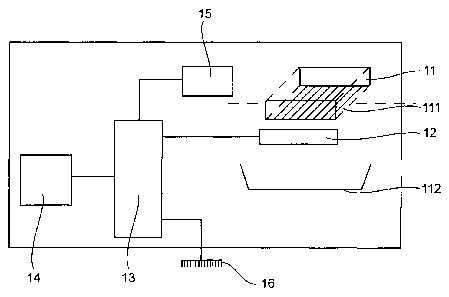
Referring to Figure 1, we present the general structure of a protection
device 10 according to the invention. Such a device comprises first of all a
capacitive detector 12 belonging to a volume defined by a first ground plane
111
of an electronic printed circuit 11 and a second ground plane of a printed
circuit
112 positioned at the bottom of the casing of the payment terminal.
These ground planes produce an action comparable to that of a Faraday
cage, i.e. they protect the protection device from external electromagnetic
disturbances if any.
The ground plane positioned at the bottom of the casing of payment
terminal is obtained for example by means of a known method for applying
conductive paint.
Besides, the calibration means 15, which are electrically connected to the
capacitive detector, enable its reference capacitance to be evaluated. These
calibration means 15 shall be described in further detail here below.
I
CA 02752311 2011-09-14
8
Furthermore, the protection device according to the invention also includes
a capacitive measurement microprocessor 13 electrically connected to the
capacitive detector 12 and to the ground 16. A measurement microprocessor of
this kind uses for example a capacitive sensor corresponding to a probe to
measure the capacitance of the capacitive detector.
Such a probe is generally made with a flat measurement electrode
surrounded by a guard ring. The electrode then, along with the capacitive
detector,
forms a flat capacitor. A guard electrode contained in the guard ring is
placed
around the measurement electrode and its potential is carried to the same
value in
order to improve linearity, by making the field lines normal (i.e.
perpendicular) to
the measurement electrode. The guard electrode thus eliminates edge effects.
Through these measurement means 13, a variation is detected in the
capacitance of the capacitive detector. This variation is obtained for example
by
comparing the measured capacitance with the reference capacitance
preliminarily
determined by the calibration means 15. This measurement is preferably done in
real time so that the secured processor of a payment terminal is
instantaneously
alerted through transmission means 14.
Independently of the measurement frequency selected by the user, all the
measurements are driven by a computer program recorded within the
measurement means.
More specifically, the measurement means determine a difference between
the capacitance of the capacitive detector measured by the measurement means
13
and the reference capacitance determined by the calibration means. If the
absolute
value of this difference exceeds a predetermined threshold S, the transmission
means of the protection device according to the invention tells the secured
processor of the secured terminal to go into "attack" mode.
Thus, the protection device according to the invention is used to determine
any contact with the capacitive detector placed in a volume defined by the
ground
plane 111 of the electronic printed circuit board 11 and by the second ground
plane 112 positioned at the bottom of the casing of the payment terminal to be
CA 02752311 2011-09-14
9
protected. In particular, any intrusion (even without direct contact with the
sensor)
by a malicious third party will be detected, because this intrusion,
especially
through the introduction of a conductive element, significantly modifies the
capacitance of the capacitive detector.
Furthermore, this protection device makes use of the capacitive detector
and of the capacitive measurement by avoiding implementation of a complex
geometrical routing or again by avoiding the use of a protective hardware
which
can easily deteriorate and is costly, for example flexible wire mesh.
Means for calibrating the considered capacitive detector
The calibration implemented by the calibration means 15 is needed
because the value of the capacitance is sensitive to external variations.
Indeed, it is known that the value of the capacitance varies according to
different factors. For example, the capacitance of a capacitive detector
varies as a
function of the charge hysteresis due to the magnetizing of a material, the
effect of
a battery of the payment terminal, or again the temperature, humidity, aging
especially by oxidation of the materials constituting the capacitive detector,
etc.
Figure 2, representing an example of calibration curves of the protection
device according to the invention, represents the procedure implemented by the
calibration means delivering the reference capacitance of the capacitive
detector.
The calibration means measure 21 (for example similarly to the method
used by the previously described measuring means) the capacitance of the
capacitive detector as a function of time. The measurement curves 21 shown in
Figure 2 attests to the fact that the capacitance varies according to time,
especially
as a function of the ambient temperature.
The calibration means take the average of the capacitance measurement
data on the measurement curve so that a reference value Ref is obtained.
Furthermore, the calibration means determine for example a capacitance
variation threshold S beyond which the variation in capacitance is abnormal.
Thus, the calibration means determine the range of values of capacitance
centered
CA 02752311 2011-09-14
on the reference value making it possible to attest to "normal" and secured
operation of the printed circuit board of the payment terminal.
Preferably, the reference value and the predetermined threshold S are
recorded in a memory and transmitted to the measurement means so these means
5 determine an intrusion by a malicious third party aiming at damaging the
electronic printed circuit board.
Optionally, the calibration means furthermore include a system of
environmental compensation aimed at adapting the reference values and the
predetermined threshold S as a function of a parameter selected by the user of
the
10 payment terminal.
For example, since the ambient temperature in Singapore is very different
from the temperature in Stockholm, the user will adapt the capacitance
reference
and the authorized range of capacitance variation to the location.
Similarly, in another example, the user may adapt this range of variation as
and when the payment terminal ages, according to the manufacturer's
recommendations set forth in a user's instruction sheet.
5.2 Description of a first embodiment of a device according to the
invention
Structure of the protection device according to this first embodiment
In this embodiment, represented by Figures 3A to 3D, we present a
protection device according to the invention in which a first capacitive
detector is
mounted on the memory card connector shown in Figure 3A.
The first capacitive detector placed on the memory card connector
measures the capacitance of the volume defined by a first ground plane Ill of
an
electronic printed circuit board 11 and a second ground plane 112 positioned
at
the bottom of the casing of the payment terminal.
Thus, any insertion of an object, even very small, formed by one or more
conductive parts, between the capacitive detector and one of the ground planes
(defining the volume containing the capacitive detector) modifies the field
lines
32 shown in Figure 3B.
I
CA 02752311 2011-09-14
11
This modification of field lines leads to a variation of the capacitance of
the volume beyond the predetermined threshold defined previously by the
calibration means.
Type of capacitive detector
A capacitive detector taking the form of a simple copper track is used for
example and shown in Figure 3C. This track takes for example the shape of a
square spiral 33.
According to another variant, the detector 12 corresponds to a full plane 34
and is positioned on a surface of the memory card connector of the payment
terminal for example.
A capacitive detector corresponding to a full plane takes the form of a
capacitive surface. More specifically, a capacitive surface technology
consists of a
uniform conductive coating on an insulator. During use, electrodes placed on
the
edge of the insulator distribute a low-voltage current equally throughout the
conductive layer, thus creating a uniform electric field. When an object comes
into contact with the surface, it has the effect of attracting the current
from each
corner of the electrical field.
Optionally, a controller computes the coordinates of the contact by
measuring the current. It then transmits these coordinates to the secured
processor
of the payment terminal.
In another embodiment, the capacitive detector may take the form of a
lattice (not shown) of very fine (smaller than 10 m) conductive wires buried
between layers of insulator, for example glass or laminated plastic films.
A lattice of this kind may be plane or three-dimensional with a mesh of
greater or lesser density. A single wire, positioned in a particular way, may
also
be sufficient in certain examples.
Furthermore, the protection device of the invention can also be electrically
connected to a printed circuit board having an existing capacitive detector
constituted by a conductive part and an insulator part. In this case, the
protection
device of the invention has electrodes placed on the edge of the insulator in
order
CA 02752311 2011-09-14
12
to distribute a low-voltage current equally throughout the whole conductive
part,
thus creating a uniform electrical field. The existing detector is thus made
capacitive.
5.3 Description of a second embodiment of a --device according to the
invention
Referring to Figure 4A, we present the drawing of a second embodiment
of the invention. This second embodiment, in addition to the first capacitive
detector 41 placed on the memory card connector, adds a second capacitive
detector in order to prohibit access to the links of the memory card
connector,
especially the MC_IO link (memory card input/output link).
As illustrated in Figure 4A, the memory card connector 42 is mounted on
the printed circuit board 43. The memory card connector has a slot 42.1 into
which the card can be inserted. The memory card connector also has a set of
links
42.2 enabling a connection of the card, once inserted, with a processor of the
apparatus.
These links 42.2 have a slight bulge 42.3 in the zone of connection with
the card, within the memory card connector. The links are then easily shaped
so
that they stretch towards the printed circuit board 43. They meet this printed
circuit board at an intermediate zone in which the links 42.4 are connected to
the
printed circuit board 43.
The second capacitive detector 44 is laid out so that it prevents access to at
least certain links and especially to the MC_IO link.
An electronic structure of the second capacitive device is shown with
reference to Figure 4B. In this structure, a linking capacitor CL implements a
capacitive coupling making it possible to evaluate the capacitance of the
MC_IO
link. Furthermore, this detector is powered with a nominal voltage Vcam and
also
comprises a resistor R and a stray capacitance CP.
Vcam and R depend on the terminal and more particularly on the EMV
standards and are present in all payment terminals. The linking capacitance CL
is
CA 02752311 2011-09-14
13
directly related to the invention, it has a value of 220 pF (by way of an
indication)
and this value can vary as a function of the dimensions of the tracks.
5.4 Description of an embodiment of the method of protection according
to the invention
Referring to Figure 5, we present the method 50 for protecting an
electronic printed circuit board according to the invention.
Such a method comprises
- a step 51 for placing at least one capacitive detector on a layer of
the printed circuit board of the payment terminal,
- a calibration step 52 delivering the reference capacitance of the
capacitive detector,
- a step 53 of capacitive measurement implemented by a capacitive
measurement microprocessor electrically linked to the capacitive
detector, the microprocessor being configured to detect a variation
in capacitance of the capacitive detector
a step 54 for transmitting a piece of information "Attack!"
representing the variation in capacitance when an absolute value of
a difference between the measured capacitance and the reference
capacitance exceeds a predetermined threshold.
Furthermore, a calibration step could be reiterated for a procedure of
utilization known by the user.
According to one particular embodiment, the calibration step furthermore
comprises a step of environmental compensation aimed at taking into account
the
natural influence of certain parameters such as: the charge hysteresis due to
the
magnetization of a material, the effect of a battery of the payment terminal,
or
again the temperature, humidity, aging especially by oxidation of the
materials
constituting the capacitive detector, etc.
The protection method implemented by a protection device compliant with
the second embodiment described here above, implements two capacitive
detectors, one being placed on the memory card connector and one being
CA 02752311 2011-09-14
14
connected to the input/output link of the memory card connector. The steps of
the
method described here above are therefore performed for each capacitive
detector
implemented.
Referring now to Figure 6, we present an embodiment of a payment
terminal according to the invention.
Such a terminal comprises a memory 61 constituted by a buffer memory, a
processing unit 62, equipped for example with a microprocessor P, and driven
by
the computer program 63 implementing the method of protection according to the
invention.
At initialization, the code instructions of the computer program 63 are
loaded for example into a RAM and then executed by the processor of the
processing unit 62. The processing unit 62 inputs at least one piece of
information
I, such as the location zone identifiers. The microprocessor of the processing
unit
62 implements the steps of the protection method described here above,
according
to the instructions of the computer program 63 to deliver a piece of processed
information T such as the detection of an attack leading to the elimination of
the
protected data. To this end, in addition to the buffer memory 61, the terminal
comprises at least one capacitive detector placed in a volume formed by a
first
ground plane of said printed circuit and a second ground plane positioned on
an
internal surface of said casing, said at least one capacitive detector being
configured to deliver a reference capacitance, a capacitive measurement
microprocessor electrically connected to said at least one capacitive
detector, said
at least one microprocessor being configured to detect a variation in
capacitance
of said at least one capacitive detector, means for transmitting a piece of
information representing said variation in capacitance, when an absolute value
of
a difference between said measured capacitance and said reference capacitance
exceeds a predetermined threshold.
These means are driven by the microprocessor of the processing unit 62.