Note : Les descriptions sont présentées dans la langue officielle dans laquelle elles ont été soumises.
CA 02752486 2011-08-12
WO 2010/095955 PCT/N02010/000069
HIGH VOLTAGE TRANSFORMER
This invention relates to a high voltage transformer. More
particularly it concerns a high voltage transformer for
cascade connection where the high voltage transformer
comprises a primary winding, a high voltage winding and a
transformer core and wherein the primary winding and the high
voltage winding encircles at least a part of the transformer
core.
In the description the term "good high frequency qualities"
is used. By this is meant that a so-called "pulse trans-
former" having relatively low coupling inductance between the
primary and secondary windings, relatively low so-called
"skin effect" and "proximity effect" in the windings at
relatively high frequencies, relatively low parasitic
capacitance internally in the windings and relatively low
capacitance between windings and between windings and the
transformer core. This concerns particularly the high voltage
winding. Said physical parameters are well known to a person
well versed in the art and are therefore not explained
further.
For a pulse transformer being run near to saturation, typical
for inverters, the practical expression:
U = 4Bs*f*n*Ae
CA 02752486 2011-08-12
WO 2010/095955 PCT/N02010/000069
is used, where B3 = magnetic flux density (saturation), U =
the top value of the voltage over the winding, f = working
frequency, n = number of turns and A,, = effective cross-
section of the transformer core.
From the expression appears that a high output voltage may be
achieved at a high frequency, high saturation field strength,
large iron cross-section and many turns.
In case of little room available it is often easiest to
increase the frequency. To avoid too great eddy-current
losses one then has to use core materials having low
electrical conductivity such as ferrite, iron powder or
so-called "tape wound cores".
A method for feeding the transformer a relatively high
frequency comprises a so-called SMPS - (Switched Mode Power
Supply) technique. The input power is according to this
technique converted to a preferably square pulse high
frequency input voltage to the high voltage transformer.
A prior art high voltage transformer has as mentioned, due to
its mode of operation, a relatively high number of turns in
the secondary winding. This causes an increased secondary
capacitance in that the windings with many layers of
relatively thin winding wire have less mutual average
distance from each other than in a transformer where the
winding wire is of larger diameter.
The many turns of the secondary winding requires relatively
much space and thereby leads to the transformer core and the
primary winding being relatively large. In addition large
insulation distances are required between high voltage
winding, primary winding and transformer core. The
transformer thus being relatively large leads to increased
losses in transformer windings and also that high voltage
2
CA 02752486 2011-08-12
WO 2010/095955 PCT/N02010/000069
transformers of this kind have a relatively low coupling
factor. A low coupling factor may be modelled as a relatively
large coupling inductance. The reason is that a relatively
large distance between the primary and secondary windings
leads to poor magnetic coupling between them.
This unintentional and in the main unavoidable parasitic
coupling inductance will, in the same way as the secondary
capacitance and in combination with the secondary
capacitance, influence the current in the transformer. By the
coupling inductance limiting the high frequent current, and
also that most of this current is used to drive internal
parasitic capacitance in the secondary winding, a clear
limitation in the power output from the secondary winding at
high frequencies arises. High frequency transformers of this
is kind have thus a relatively narrow bandwidth, i.e. the
highest driving frequency the high frequency transformer can
work at.
Known low voltage SMPS technique can produce voltages up to
the order of 1 kV. At higher voltages it is necessary to
adapt the transformer by means of per se known techniques as
voltage multiplication, cascade coupled high frequency
transformers, layered winding techniques or so-called
"resonant switching" to compensate for the relatively narrow
bandwidth in a high frequency transformer.
Common for all these techniques is that they only to a
limited extent overcome the drawbacks at the same time as
they complicate and thereby raise the price of the complete
high frequency converter.
It is known to reduce the number of layers in a transformer
to be able to achieve improved transformer properties. US
patent 7274281 deals with a transformer for a discharge lamp
3
CA 02752486 2011-08-12
WO 2010/095955 PCT/N02010/000069
such as a fluorescent tube where the transformer is provided
with two series connected primary windings that may be
constituted by one winding layer.
US 1680910 describes a transformer for cascade connection.
This one is however not suitable for SMPS because it has a
high capacitance in the windings and a low coupling factor.
US 4518941 shows a transformer that is suitable for SMPS but
where the rated transformer ratio is one to one. The
transformer according to this document is not suitable as a
high voltage transformer.
US 3678429 shows a high voltage transformer for cascade
coupling wherein there besides a primary winding and a
secondary winding is arranged a winding for cascade coupling.
Due to the design of the high voltage winding the transformer
is according to US 3678429 is not suitable for SMPS.
US 3579078 deals with a one-step transformer coupled to a
so-called "Voltage Quadrupler". The transformer does not
however solve the relevant technical problem as one does not
achieve a high enough voltage in one step.
From WO 2007045275 it is known to use two secondary windings
for cascade coupling with a so-called "flyback-convertor" to
achieve a stable output voltage in each cascade step.
Prior art does not exhibit transformers having suitable high
voltage properties and at the same time being suitable for
cascade coupling.
The object of the invention is to remedy or reduce at least
one of the prior art drawbacks.
4
CA 02752486 2011-08-12
WO 2010/095955 PCT/N02010/000069
The object is achieved according to the invention by the
features stated in the below description and in the following
claims.
There is provided a high voltage transformer for cascade
s coupling where the high voltage transformer comprises a
primary winding, a high voltage winding and a transformer
core and where the primary and high voltage windings
encircles concentrically at least a part of the transformer
core, and which is characterised in that the high voltage
transformer is provided with a secondary winding as the high
voltage winding comprises one single layer or more parallel-
connected single layers.
In the high voltage transformer according to the invention
the voltage over the primary and the secondary winding is
low-tension relative to the high voltage winding. The
secondary winding is arranged to carry a larger power than
the high voltage winding.
The high voltage winding is also a secondary winding, but the
term high voltage winding is used to better differentiate
this winding from the relatively low-voltage secondary
winding.
By winding the high voltage winding in a tubular single
layer, internal parasitic capacitance in the high voltage
winding is reduced to a practical minimum. To reduce the
resistance in the high voltage winding several layers may be
wound one outside of the other where the layers thereafter
are connected in parallel, for example in the conductor
portions of the high voltage winding. It may be expedient to
arrange insulation sheeting, for example polyamide film
between the layers. In a multi-layer high voltage winding of
this kind, one will still achieve getting the internal
5
CA 02752486 2011-08-12
WO 2010/095955 PCT/N02010/000069
capacitance small relative to known high voltage windings
being wound back and forth in more layers connected in
series.
Between the primary and secondary windings there may be an
annular opening for cooling fluid running therethrough. Such
an opening between the windings and the transformer core
ensures at the same time the necessary insulation distance
and results in relatively low capacitance between windings
and between windings and the transformer core.
io By the high voltage winding being tubularly wound and axially
outside the primary winding and also normally concentric with
it, a relatively high coupling factor between the windings is
achieved. The leak inductance between the windings is thereby
almost negligible.
is The series resonant frequency f, ,of a transformer is given
by:
Ls _ prim := Lm(1 - kp2 )
Nsek 2
Cp-prim Cs
Npnm
2n L C
sjrim pjrim
20 Where Lm is primary magnetising inductance, kp is coupling
factor, Nsek and Nprim number of turns on secondary and primary
winding respectively. Cg is total parasitic capacitance in
the secondary winding. The series resonant frequency is a
direct measure of how good the high frequency properties of
25 the transformer are.
6
CA 02752486 2011-08-12
WO 2010/095955 PCT/N02010/000069
According to prior art it is common to fill the so-called
winding window of a transformer with windings to reduce
resistance and conductor losses. A high voltage winding with
its relatively large volume usually takes up a considerable
share of this winding window. To arrange a high voltage
winding in just one layer is thus violating known principles
for transformer design.
Even if according to the invention only one layer is used in
the high voltage winding it is necessary to use a relatively
large number of turns in the high voltage winding relative to
the primary winding to be able to achieve a suitable voltage
increase. By the very fact that the high voltage winding
should have the same overall length as the primary winding,
and that these are limited by the winding window, a
relatively thin conductor needs therefore to be used in the
high voltage winding. This entails a relatively high
resistance in the high voltage winding conductor and that the
high voltage winding gets the form of a thin pipe. The
relationship is compensated by that the transformer may be
made relatively small, whereby the length of each turn is
reduced. The resistance is also reduced thereby.
If this kind of high voltage transformer is used in a cascade
coupling, the power requirement is reduced in each high
voltage winding as shown in the following formula:
Psek_M =P
M
rint_ll 1 )
N
Where M is the number of the relevant step and N is number of
steps.
The high voltage winding being wound of a relatively thin
winding wire limits the power it can supply. This drawback is
compensated to a considerable extent by that a transformer
7
CA 02752486 2011-08-12
WO 2010/095955 PCT/N02010/000069
according to the invention has a considerably improved
efficiency compared to prior art transformers, and that the
thin winding wire makes room for a cooling slit between the
windings and between the windings and the transformer core
s making good cooling and electric insulation between the
components possible.
If the transformer according to the invention is used in a
cascade coupling as described above, the power trough-put in
the high voltage winding is reduced considerably relative to
prior art, whereby the drawback with high resistance in the
high voltage winding is remedied further. This makes the high
voltage transformer according to the invention suitable for
feeding from an SMPS.
The high voltage winding may be between the primary winding
is and the secondary winding in the high voltage transformer.
By connecting a first transformer secondary winding in series
with a second transformer primary winding and connecting the
high voltage winding of the first transformer in series with
the high voltage winding of the second transformer with
intermediate rectification, the voltage over the high voltage
windings are added while a part of the power between the
first transformer and a second transformer is transferred by
means of the secondary winding of the first transformer and
not via the high voltage winding of the first transformer.
The high voltage apparatus may thus comprise two or more
cascade coupled transformers. The power output on the high
voltage side thereby divides itself on high voltage windings
in more steps, where most of the steps must be rectified
before series connection to avoid that the high voltage
winding in one step must drive parasitic capacitance in
windings in the next step.
8
CA 02752486 2011-08-12
WO 2010/095955 PCT/N02010/000069
That more high voltage windings in this way share the total
output power causes that each high voltage winding may be
dimensioned for a fraction of the output power, as the number
of steps decide the fraction factor.
Increasing the output voltage intentionally further, or to be
able to reduce the number of turns to make room for a thicker
winding wire, the high voltage winding of the first trans-
former may cooperate with a voltage multiplier of a per se
known kind. The second transformer and further transformers
io in the cascade coupling may also cooperate with each of their
own voltage multiplier.
A high voltage winding with only one layer contributes to an
increased insulation distance between the layers in that the
high voltage winding takes up little room. The thin tubular
design of the windings contributes to good cooling of both
windings and transformer core, and renders the transformer
possible to handle a relatively high power relative to its
physical size. By the inner parts being cooled well in this
way, and also that internal heating in one-layer windings is
avoided, the transformer is also suitable for use under
relatively high ambient temperatures.
More transformers interconnected in a cascade coupling
according to the invention is suitable both for high voltage
direct current and a combined direct and alternating current
output, as one step may be designed without rectification.
Since primary driving voltage is conducted via low voltage
windings through all steps, it is possible to use this
alternating voltage to drive one or more additional
transformers in a high voltage cascade having differently
rated transformer ratios between the windings to generate
different voltages that may be needed in a system. A
9
------------
CA 02752486 2011-08-12
WO 2010/095955 PCT/N02010/000069
secondary voltage on the last step may for example drive an
additional transformer generating filament voltage for an X-
ray tube. If so, this is a separate low voltage alternating
voltage or a rectified alternating voltage superimposed on
the high voltage.
The transformer of the invention is particularly suitable for
use in miniature high voltage power supplies. It occupies
relatively little room, puts up with relatively high ambient
temperatures and may be formed having a lengthy cylindrical
shape, and where there is a need for high voltage direct
current or high voltage direct current with superimposed
alternating current.
The transformer may thus suit applications such as in
petroleum wells, spraying plants, X-ray apparatuses,
electrostatic precipitators and non-thermal plasma
generating.
In the following is described an example of a preferred
embodiment being illustrated in the accompanying drawings,
wherein:
Fig. 1 shows in perspective a high voltage transformer ac-
cording to the invention;
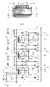
Fig. 2 shows a section I-I in fig. 1;
Fig. 3 shows a circuit diagram for a cascade coupled high
voltage apparatus with voltage multipliers;
Fig. 4 shows a printout of a typical voltage signal level
during operation in the first step according to the
circuit diagram in fig. 3;
CA 02752486 2011-08-12
WO 2010/095955 PCT/N02010/000069
Fig. 5 shows in perspective a high voltage apparatus ac-
cording to the circuit diagram in fig. 3 for enclo-
sure in a cylindrical cavity; and
Fig. 6 shows a circuit diagram for a cascade coupled high
voltage apparatus in a simplified embodiment.
In the following indexed reference numerals are used when the
reference numeral relates to a specific component from
several components of the same kind such as transformers. In
the drawings are more indexed reference numerals shown
without each indexed reference numeral necessarily being
mentioned in the description.
In the drawings the reference numeral 1 indicates a high
voltage apparatus with a transformer 2. The transformer 2
comprises two opposing E-shaped ferrite transformer cores 4
where about and spaced from the mid portions 6 of the
transformer cores 4 is coiled a primary winding 8 on a
cylindrical, insulating primary sleeve 10. The first
conductor end portion 12 and the second conductor end portion
14 of the primary winding 8 are led out on the same end
portion of the primary winding 8.
A high voltage winding 16 encircles the primary winding 8 at
a radial distance. The high voltage winding 16 is wound in
one layer on a cylindrical, insulating high voltage sleeve
18. The first conductor end portion 20 and the second
conductor end portion 22 of the high voltage winding 16 are
led out on one each end portion at the high voltage winding
16.
A secondary winding 24 encircles the high voltage winding 16
at a radial distance. The secondary winding 24 is wound on a
cylindrical, insulating secondary sleeve 26. The first
conductor end portion 28 and the second conductor end portion
11
CA 02752486 2011-08-12
WO 2010/095955 PCT/N02010/000069
30 of the secondary winding 24 are led out on the same end
portion at the secondary winding 24.
In figs. 1 and 2 the secondary winding 24 is also encircled
by a static-shield winding 32 connected to the transformer
core 4. Preferably the static-shield winding 32 encircles
most of the secondary winding 24, but not completely
encircling this, as this if so would constitute a
short-circuit turn for the transformer 2. The static-shield
winding 32 is arranged to improve the high voltage insulation
relative to in figs. 1 and 2 adjacent and not shown
components.
The primary winding 8 and the secondary winding 24 have
approximately the same number of turns, while the high
voltage winding 16 has a considerably higher number of turns.
The different windings are interconnected by means of not
shown per se known circuit board electrical path.
The transformer 2 is suitable for being fed with an inverted
direct voltage from an SMPS power source 34 connected to the
first conductor end portion 12 and the second conductor end
portion 14 of the primary winding 8 corresponding to what is
shown in the diagram in fig. 3. Thus an alternating voltage
may be taken out on the first conductor end portion 20 and
the second conductor end portion 22 of the high voltage
winding 16 and an alternating voltage corresponding to the
feed voltage on the first conductor end portion 28 and the
second conductor end portion 30 of the secondary winding 24.
The circuit diagram in fig. 3 shows that the high voltage
apparatus 1 in this embodiment besides a first transformer 21
also comprises a second transformer 22 and a third
transformer 23. The second transformer 22 and the third
12
CA 02752486 2011-08-12
WO 2010/095955 PCT/N02010/000069
transformer 23 have the same design as the first transformer
21.
The SMPS power source 34 is connected to the first conductor
end portion 121 and the second conductor end portion 141 of
the primary winding 81 of the first transformer 21. The sec-
ondary winding 241 of the first transformer 21 is by means of
the first conductor end portion 281 connected to the first
conductor end portion 122 on the primary winding 82 of the
second transformer 22. The second conductor end portion 30,
of the secondary winding 241 is correspondingly connected to
the second conductor end portion 142 of the primary winding
82.
The same applies between the second transformer 22 and the
third transformer 23. The first conductor end portion 282 of
the secondary winding 242 is connected to the first conductor
end portion 123 of the primary winding 83 and the second
conductor end portion 302 of the secondary winding 242 is
connected to the second conductor end portion 143 of the
primary winding 83-
The first conductor end portion 283 and the second conductor
end portion 303 of the secondary winding 243 of the third
transformer 23 are connected together to a so-called dummy
load 36 having a relatively large electrical resistance. All
the second conductor end portions 221, 222, 223 of the high
voltage windings 161, 162, 163 are connected to the
corresponding transformer core 41, 42, 43 constituting local
0-levels.
The SMPS power source 34 is earthed to an earth point 38.
A first condenser 401 is connected to the first transformer
21 between the second conductor end portion 221 and the earth
point 38 of the high voltage winding 161. A first anode of
13
CA 02752486 2011-08-12
WO 2010/095955 PCT/N02010/000069
diode 421 is also connected to the earth point 38. The first
cathode of the diode 421 is connected to the anode of a
second diode 441 and via a second condenser 461 to the first
conductor end portion 201 of the high voltage winding 161.
The cathode of the second diode 441 is connected to the anode
of a third cathode 481 and to the second conductor end
portion 221 of the high voltage winding 161 and thereby to the
transformer core 41 constituting the local 0-point.
The cathode of the third diode 481 is connected to the anode
of a fourth diode 501 and to the first conductor end portion
201 of the high voltage winding 161 via a third condenser 521.
The cathode of the fourth diode 501 is connected to the
second conductor end portion 301 of the secondary winding 241
and to the second conductor end portion 221 of the high
voltage winding 161 via a fourth condenser 541.
The diodes 421, 441, 481, 501 and the condensers 401, 461, 521,
541 thus constitute a voltage multiplier 561 of a per se known
design.
The second transformer 22 is correspondingly provided with a
second voltage multiplier 562, but here is the first
condenser 402 and the anode of the first diode 422 connected
to the second connector end portion 142 of the primary
winding 82.
In the same way is the third transformer 23 correspondingly
provided with a third voltage multiplier 563, where the first
condenser 403 and the anode of the first diode 423 is
connected to the second connector end portion 143 of the
primary winding 83.
14
P, S70nPrnnnP
CA 02752486 2011-08-12
WO 2010/095955 PCT/N02010/000069
A load 58 is connected between the second connector end
portion 303 of the secondary winding 243 of the third
transformer 23 and the earth point 38.
The first transformer 21 constitutes together with the first
voltage multiplier 561 a first step 601 in the high voltage
apparatus 1. The second transformer 22 constitutes together
with the second voltage multiplier 562 a second step 602 and
the third transformer 23 constitutes together with the third
voltage multiplier 563 a third step 603-
When a drive voltage, here in the form of an inverted direct
voltage from the SMPS power source 34, is supplied to the
primary winding 81 of the first transformer, a share of the
power is taken out in the high voltage winding 161 and the
balancing part out in the secondary winding 241. The
secondary winding 241 also contributes to stabilise the
voltage over the first step 601. The ratio of the power
output in the high voltage winding 161 to the secondary
winding 241 is controlled as described in the general part of
the description.
The alternating voltage from the secondary winding 241 and
the rectified high voltage from the high voltage winding 161
in the first step 601 is conducted to the second step 602 via
a common conductor as it is shown in the circuit diagram in
fig. 3. The high voltage winding 163 does not conduct the
high voltage to further steps. Neither does the secondary
winding 243 conduct primary drive voltage to further steps.
Nevertheless is this high voltage output voltage connected
via the secondary winding 243 for the internal charging and
voltage split in the transformer 23 to be equal to the rest
of the transformers 21, 22, and to be able to build the
transformer 23 with appurtenant components equal to the rest
of the transformers 21, 22.
CA 02752486 2011-08-12
WO 2010/095955 PCT/N02010/000069
To get the highest possible voltage over each step 60 with
the fewest possible turns in the high voltage windings 161,
162, 163, each step 601, 602, 603 comprise their respective
voltage multipliers 561, 562, 563-
The connection shown effects that there in the first step 601
arises a doubling of negative top voltage at the anode of the
first diode 421 relative to the top voltage of the high
voltage winding 161, and a doubling of positive voltage on
the cathode of the fourth diode 501 relative to the top
voltage of the high voltage winding 161. The first condenser
401 stores and stabilises the double negative voltage while
the fourth condenser 541 stores and stabilises the double
positive voltage. The first condenser 401 and the fourth
condenser 541 are connected to the local 0-level, which also
1s the second conductor end portion 221 of the high voltage
winding 161 and the transformer core 41 are connected to.
The third condenser 521, the third diode 481 and the fourth
diode 501 generate a double positive top voltage while the
second condenser 461 together with the first diode 421 and
the second diode 441 generate a double negative top voltage.
The rectified high voltage from the first step 601 is fed
further into the second step 602 where it is added to the
voltage from the second step 602 and on to the third step 603
wherefrom the summed up voltage from the three steps 601,
602, 603 are supplied to the load 58.
In fig. 4 is shown a graph wherein the abscissa shows the
time in ps, and the ordinate shows the voltage in Volt. The
curves 62 and 64 show primary voltage at 100kHz and 1kV
amplitude. The curve 62 is shown in dotted line and in a
narrower line compared to the curve 64. The curve 66 shows
16
CA 02752486 2011-08-12
WO 2010/095955 PCT/N02010/000069
alternating voltage over the high voltage winding 161. The
curve 68 shows a relatively stable voltage at local 0-level,
i.e. on the second conductor end portion 221 of the high
voltage winding 161, and the curve 70 shows a doubling of
positive top voltage on the cathode of the fourth diode 501
compared to the local 0-level.
Negative double top voltage is in the first step 601
connected to the earth point 38 being the real 0 in the
graph.
The curves 62-70 in fig. 4 concerns a high voltage apparatus
1 wherein the voltage over each step 60 is 17kV and the
voltage output from the high voltage apparatus 1 is 51kV. The
load 58 is 500 kohm, and output power is about 5kW.
A practical construction of the high voltage apparatus 1 for
placement in a not shown cylindrical space is shown in fig.
5. Connector paths are not shown. The windings 8, 16 and 24
are connected to a winding circuit card 72 wherefrom the not
shown connectors run via the not shown connector paths via
plate card 74 and disc card 76 as described above to the rest
of the components of the high voltage apparatus 1.
Due to space considerations two condensers connected in
parallel in Fig. 5 constitute each condenser in the circuit
diagram in fig. 3. In the same way every diode in the circuit
diagram in fig. 3 is constituted by two diodes connected in
series in fig. 5.
Fig. 6 shows a simplified embodiment of the high voltage
apparatus 1 wherein the voltage multipliers are left out, as
the first condensers 401, 402, 403 and the fourth condensers
54 may be constituted by the internal capacitance of the high
voltage windings 161, 162, 163-
17
CA 02752486 2011-08-12
WO 2010/095955 PCT/N02010/000069
The high voltage apparatuses 1 in fig. 3 and 4 give a
positive output voltage. If all diodes are turned, a negative
output voltage is given off.
18