Note : Les descriptions sont présentées dans la langue officielle dans laquelle elles ont été soumises.
CA 02754724 2012-04-27
WO 2004/029994 PCT/US2003/029224
METHODS OF FILLING VIAS IN A SUBSTRATE
BACKGROUND
Field of the Invention
[0001] The present invention relates to the field of semiconductor fabrication
technology.
[0002] The present invention relates in particular to the formation of
substrates having
multiple layers, i.e., the formation of multilayer substrates.
Description of Related Art
[0003] Multilayer substrates are becoming increasingly popular in the
microelectronics
arena for a variety of reasons. The high packing densities, accommodation of
varied types of
circuit elements and facilitation of complex circuitries afforded by
multilayer substrates have
generated an increased interest and use in these devices. As the requirements
for increased
packing densities, complex circuit functionality and other requirements
necessitated by current
market conditions proliferate, so too will the demand for multilayer
substrates that enable such
requirements.
1
CA 02754724 2011-09-28
WO 2004/029994 PCT/US2003/029224
[0004] A number of techniques currently exist for multilayer substrate
fabrication.
One method of fabricating multilayer substrates is to laminate single, unfired
semiconductor
tapes, commonly referred to in the industry as "green sheets" or "green tape."
In a typical,
conventional layered green sheet process, a multilayer substrate may be
produced by a)
printing a circuit pattern on a glass or ceramic green sheet; b) laminating
several green sheets
that have been printed; and c) firing or sintering the laminated green sheets
in a reducing
atmosphere. The resulting product is a laminated, multilayer substrate that
may be used in a
variety of applications.
[0005] Multilayer substrates formed from green sheets have a number of
disadvantages. Although any number of green sheet layers may be laminated
together, the
overall height of the multilayer substrate is determined by the thickness of
each individual
green sheet used in the multilayer structure. Green sheet thickness is
determined by the green
sheet manufacturer, and, typically, the thickness of an individual green sheet
is in the area of
6 mils to 30 mils. Most conventional multilayer substrate fabrication
techniques cannot
accommodate green sheets of less than 6 mil thickness because green sheets of
these
thicknesses tend to be too thin to be successfully fabricated into a
multilayer substrate. Thus,
where a multilayer substrate having thin layers is desired, green sheets are
generally not
feasible as an option.
[0006] Also, because the end user has no control over the thickness of each
individual
green sheet, the end user is forced to limit the number of layers of the
multilayer substrate
according to the maximum height allowable for the intended application of the
multilayer
substrate device. For applications requiring minimum substrate height, the
number of green
sheets available for lamination may be limited due to their predetermined
thickness, thus
limiting the complexity of the design. Accordingly, for small footprint
devices that require
complex designs, laminated green sheets may prove inadequate.
[0007] Another disadvantage of using laminated green sheets for multilayer
substrate
fabrication is that the green sheets must be sintered, or fired during the
fabrication process.
As is the case with many physical processes requiring the introduction of
heat, firing the
laminated green sheet, i.e., heating the green sheet, causes shrinkage in the
various elements
of the substrate, including the circuit traces printed on each laminate. Thus,
the tolerances,
dimensions and other parameters of the traces and other elements of the
substrate are subject
2
CA 02754724 2011-09-28
WO 2004/029994 PCT/US2003/029224
to variance. Moreover, the exact amount of shrinkage during firing may be
difficult to
control. For designs in which geometries are critical, requiring minimum
variance in trace
tolerances and high accuracy in trace dimensions or other substrate
parameters, laminated
green sheets may prove wholly inadequate. If a multilayer substrate is
fabricated using green
sheets in which each of the individual green sheets have thicknesses of
varying heights, a
technique which is common in the semiconductor industry, the effects of firing
and shrinkage
are even more pronounced and dramatic.
[0008] Another disadvantage of using laminated green sheets for multilayer
substrate
fabrication is that the dielectric used to form the green sheets is generally
not of as high a
quality as is required for some applications. Because multilayer substrates
fabricated with
green sheets are subjected to elevated temperatures during processing, the
dielectrics used in
green sheets must be able to tolerate elevated temperatures without compromise
to the
integrity of the dielectric. Accordingly, impure dielectrics, which typically
show enhanced
reliability at elevated temperatures, are used as the dielectric in green
sheets. These impure
dielectrics can be limiting when forming circuit elements, such as high
voltage capacitors for
example. Thus, in applications where pure dielectrics are required, the
temperature
processing required for multilayer substrates fabricated using green sheets
generally precludes
green sheets as an option for forming such substrates.
[0009] Another method of fabricating multilayer substrates is to use thick
film
processes. The thick film process is a sequential process requiring a)
printing a circuit pattern
on a substrate; b) drying the substrate; and c) firing the substrate. This
process is repeated as
many times as is necessary or desired in order to obtain the number of layers
required. Each
individual substrate is printed, dried and fired, then adhered to the other
substrates which have
been printed, dried and fired to form a substrate stack. In this way, a
multilayer substrate is
formed from individually prepared substrates.
[0010] However, multilayer substrates formed from thick film processes suffer
from
many of the same disadvantages as green sheet multilayer substrates. The
thickness of a
multilayer substrate formed using thick film processes is dictated by the
thickness of each
individual substrate. As is the case with green sheets, the ultimate height of
the substrate is
determined by the cumulative height of the substrates rather than the
requirements of the
application. Excessive cumulative substrate height may be an unacceptable
design restriction
3
CA 02754724 2011-09-28
WO 2004/029994 PCT/US2003/029224
and, thus, thick film processes may be inadequate for forming multilayer
substrates in the
intended application.
[0011] Because thick film processes require firing each substrate layer,
multilayer
substrates formed using thick film processes also suffer from shrinkage
issues. Like green
sheets, designs requiring minimum variance in substrate parameter tolerances
and high
accuracy in substrate parameter dimensions may not be adequately served by
thick film
multilayer substrate formation processes.
[0012] The filling of vias in the substrate is a normal part of the substrate
fabrication
process. Traditional via filling is usually accomplished using thick film
printing techniques,
where squeegee printing processes push conductive ink into the vias, or with
vacuum
techniques that effectively pull conductive ink through the vias.
[0013] When conductive ink is pulled through a via, much of the ink is lost
due to
waste. For small production runs, such waste maybe of little concern. However,
for large
production runs, the cost attributed to wasted ink could ultimately exceed the
cost of the
substrate itself Thus, for large production runs, filling substrate vias using
vacuum
techniques becomes cost prohibitive.
[0014] Although there is less waste in thick film techniques, traditional
squeegee via
filling techniques typically allow air to be trapped in the conductive ink,
causing air voids to
form within the interior of the via. Air voids are deleterious to the
conductive path through
the via, plaguing the via with a variety of performance detractors. Air voids
can greatly
reduce the electrical conductance through the path, increasing via resistance
and generating
excess heat in the via. To complicate matters, air voids can greatly reduce
the thermal
conductance through the path, providing even less of a mechanism by which to
remove the
excess heat resulting from the decrease in electrical conductance.
[0015] Of equal if not greater concern for practitioners involved with devices
that are
implanted into a human or animal body, air voids compromise the hermeticity of
the
conductive path through the via. Often, the conductive path through the via is
the single path
bodily fluids may take to reach sensitive microelectronics that could be
damaged or destroyed
by exposure to such fluids. If an implantable device is formed having vias
that require
hermetic sealing, any air voids within the via that compromise the hermeticity
of the path and
4
CA 02754724 2011-09-28
WO 2004/029994 PCT/US2003/029224
allow fluids to pass through the via could result in device malfunction or
even device failure,
which could have disastrous consequences for the user of the device.
[0016] Accordingly, there is a need in the semiconductor industry for
multilayer
substrates having layers which may vary widely in thickness and which may be
accurately
controlled. There is also a need in the semiconductor industry for multilayer
substrates in
which circuit element and trace tolerance is tightly controlled and line
dimension shrinkage is
minimized. There is yet another need in the semiconductor industry for
multilayer substrates
in which high purity dielectrics may be used.
[0017] In addition, there is a need in the semiconductor industry for methods
and
systems for filling vias in a substrate that do not waste conductive ink.
There is yet another
need in the semiconductor industry for methods and systems for filling vias in
a substrate that
eliminate air voids in the conductive path through the via.
SUMMARY
[0018] Accordingly, it is an object of embodiments of the present invention to
provide
a multilayer substrate and a method of fabricating a multilayer substrate in
which the
multilayer substrate may be fabricated without firing. It is also an object of
embodiments of
the present invention to provide a multilayer substrate and a method of
fabricating a
multilayer substrate in which the thickness of each layer in the substrate may
be widely varied
and accurately controlled by the user. It is also an object of embodiments of
the present
invention to provide a multilayer substrate and a method of fabricating a
multilayer substrate
in which circuit element and trace tolerance is tightly controlled and
dimension shrinkage is
kept to a minimum or eliminated altogether. It is also an object of
embodiments of the
present invention to provide a multilayer substrate fabricated using a process
in which
dielectrics of high purity may be incorporated into the substrate.
[0019] Embodiments of the present invention may use of variety of materials as
multilayer substrate dielectrics. For example, and without limitation, alumina
having a purity
of 99.999% may be used as a dielectric in embodiments of the present
invention.
[0020] According to an embodiment of the present invention, a multilayer
substrate
device includes a base substrate and a first metalization layer formed on the
base substrate,
wherein the multilayer substrate is formed without firing. The multilayer
substrate may also
CA 02754724 2011-09-28
WO 2904/02999-4 PCT/US2003/029224
include a plurality of alternating dielectric layers and metalization layers
formed over the first
metalization layer. One of the plurality of the dielectric layers may be
alumina.
[0021] The multilayer substrate may also include vias extending through one of
the
plurality of dielectric layers such that two of the metalization layers
surrounding the one of
the plurality of dielectric layers make contact with each other through the
via. Also, two of
the plurality of metalization layers and one of the plurality of the
dielectric layers may form a
capacitor.
[0022] The base substrate of the multilayer substrate maybe formed from a
variety of
materials, such as, for example, glass or ceramic.
[0023] According to an embodiment of the present invention, a method for
forming a
multilayer substrate includes obtaining a base substrate and forming a first
metalization layer
on the base substrate without firing. The method may further include forming a
plurality of
alternating dielectric layers and metalization layers over the first
metalization layer. Any
layer of the plurality of dielectric layers may be formed by a variety of
techniques, including,
without limitation, ion beam assist deposition, sputtering, chemical vapor
deposition, epitaxial
deposition or evaporation.
[0024] A method of forming a plurality of dielectric layers in the multilayer
substrate
may include forming an opening in a mask; affixing the mask to a layer of the
substrate;
depositing an active material in the openings; removing the mask after the
active material has
been deposited; forming a dielectric around the active material; and removing
the active
material after the dielectric has been formed around the active material. When
forming the
plurality of dielectric layers in the multilayer substrate, a height of the
dielectric layer is less
than a height of the active material. For example, the height of the
dielectric layer may be
one-third or one-half the height of the active material.
[0025] When forming the active material on the multilayer substrate, pillars
may be
formed on one of the plurality of metalization layers out of the active
material. The active
material may be removed using a dissolving solution, such as, for example,
ferric chloride.
After the active material is removed, vias may be formed through one of the
plurality of
dielectric layers.
[0026] It is also an object of the present invention to provide a cost-
efficient method
and apparatus for filling vias in a substrate that reduces or eliminates
wasted conductive ink.
6
CA 02754724 2011-09-28
WO 200-4/029994 PCT/US2003/029224
It is a father embodiment of the present invention to provide a method and
apparatus for
providing conductive paths through vias in a substrate that are devoid of air,
such that the path
through the via may be hermetic.
[0027] According to an embodiment of the present invention, an assembly for
fabricating substrates includes first and second pressure plates for applying
pressure, first and
second assembly plates, and first and second printing sheets for printing on a
substrate. The
first assembly plate may be located adjacent the first pressure plate and the
second assembly
plate may be located adjacent the second pressure plate. The first printing
sheet may be
located adjacent the first assembly plate and the second printing sheet may be
located adjacent
the second assembly plate. The assembly may also include an enclosure
surrounding the first
and second assembly plates, the first and second printing sheets, and the
substrate.
[0028] According to an embodiment of the present invention, the first pressure
plate
and the first printing sheet surround the first assembly plate and the second
pressure plate and
the second printing sheet surround the second assembly plate. Also, the first
pressure plate,
the first assembly plate and the first printing sheet are located adjacent a
first side of the
substrate and the second pressure plate, the second assembly plate and the
second printing
sheet are located adjacent a second side of the substrate. A pressure applied
by the first
pressure plate and the second pressure plate acts through the first assembly
plate and the
second assembly plate to force ink in the first printing sheet and the second
printing sheet
through vias in the substrate
[0029] The enclosure may include a port for pulling a vacuum in the enclosure
and,
thus, a vacuum may surround the assembly and the substrate. Also, the first
and second
printing sheets may be made from foam rubber.
[0030] According to an embodiment of the present invention, a method for
filling vias
in a substrate may include forming an assembly around the substrate, the
assembly including
printing sheets for containing a conductive ink and further including pressure
plates for
applying pressure; applying a vacuum about the assembly; and applying pressure
to the
printing sheets. When pressure is applied by the pressure plates the
conductive ink in the
printing sheets is pushed through the vias. The method may also include
printing a pattern on
the substrate; drying the substrate; and firing the substrate.
7
CA 02754724 2011-09-28
WO 20041029994 PCT/US2003/029224
[0031 ] When forming the assembly around the substrate, the method may include
positioning a first printing sheet adjacent a first side of the substrate;
positioning a first
assembly plate adjacent the first printing sheet; positioning a first pressure
plate adjacent the
first assembly plate; positioning a second printing sheet adjacent a second
side of the
substrate; positioning a second assembly plate adjacent the second printing
sheet; positioning
a second pressure plate adjacent the second assembly plate; and positioning an
enclosure
around at least the substrate and the first and second printing sheets.
[0032] Applying a vacuum about the assembly may include pulling a vacuum in
the
enclosure. When pulling a vacuum in the enclosure, air is removed from the
conductive ink
when a vacuum is pulled in the enclosure. Also, applying a pressure to the
printing sheets
may include applying a low pressure or a high pressure. The high pressure may
be about
1000 lbs.
BRIEF DESCRIPTION OF THE DRAWINGS
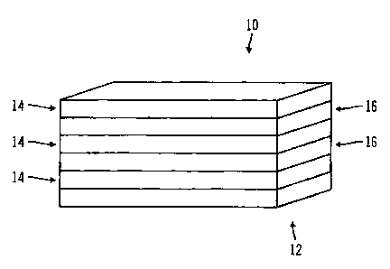
[0033] Figure 1 shows a perspective view of a multilayer substrate according
to an
embodiment of the present invention.
[0034] Figure 2 shows a generalized method for fabricating a multilayer
substrate
according to an embodiment of the present invention.
[0035] Figure 3A shows a perspective view of a base substrate according to an
embodiment of the present invention.
[0036] Figure 3B shows a plan view of a metalization layer having a metal
pattern
formed on top of a base substrate according to an embodiment of the present
invention.
[0037] Figure 4A shows a perspective view of two aluminum pillars formed and
located on top of a metalization layer according to an embodiment of the
present invention.
[0038] Figure 4B, shows a perspective view of a dielectric layer formed on top
of a
metalization layer and covering a portion of aluminum pillars according to an
embodiment of
the present invention.
[0039] Figure 4C shows a perspective view of a dielectric layer formed on top
of a
metalization layer in which the aluminum pillars have been removed according
to an
embodiment of the present invention.
[0040] Figure 5 shows a perspective view of a metalization layer deposited
onto a
dielectric layer according to an embodiment of the present invention.
8
CA 02754724 2011-09-28
WO 2004/029994 PCT/US2003/029224
[0041] Figure 6 shows a detailed method for fabricating a multilayer substrate
according to an embodiment of the present invention.
[0042] Figure 7 shows a plan view of an assembly for filling via holes in a
substrate to
an present embodiment of the invention.
[0043] Figure 8 shows a method for filling via holes in a substrate to an
embodiment
of the present invention.
DETAILED DESCRIPTION
[0044] In the following description of preferred embodiments, reference is
made to
the accompanying drawings which form a part hereof, and in which are shown by
way of
illustration specific embodiments in which the invention may be practiced. It
is to be
understood that other embodiments may be utilized and structural changes may
be made
without departing from the scope of the preferred embodiments of the present
invention.
[0045] A multilayer substrate 10 according to an embodiment of the present
invention
is shown generally in Figure 1. The multilayer substrate 10 may contain a
plurality of
alternating dielectric layers and conductive layers. As shown in Figure 1, the
multilayer
substrate 10 starts with a base substrate 12, on top of which is a
metalization, or conductive,
layer 14. The multilayer substrate 10 of Figure 1 includes two other
metalization layers 14.
Sandwiched in between the metalization layers 14 are dielectric layers 16.
[0046] The base substrate layer 12 may be rigid or flexible and may be made
from any
type of substrate material commonly used in the art, such as, for example,
ceramic, glass,
silicon, gallium arsenide, alumina and the like. The metalization layer 14 may
also be formed
from a variety of materials, such as, for example, copper, aluminum, silver,
gold, titanium,
platinum and the like. The dielectric layer 16 may be of a variety of
materials commonly
used in the art, such as, for example, ceramic, silicon, alumina and the like.
Dielectrics of
high purity may be used for the dielectric layer 16, such as, for example,
99.999% alumina.
[0047] Although the multilayer substrate 10 shown in Figure 1 may appear to
have an
extended height, the height of each layer shown in Figure 1 is exaggerated for
illustration
purposes only. In fact, the height of each layer shown in the multilayer
substrate 10 of Figure
1 may vary widely at the discretion of the fabricator.
[0048] Moreover, although the multilayer substrate 10 of Figure 1 is shown to
be a
rectangular cylinder, it need not be. Indeed, the shape of the multilayer
substrate 10 may take
9
CA 02754724 2011-09-28
WO 2004/029994 PCT/US2003/029224
on any shape desired by the fabricator. The multilayer substrate 10 may be a
rectangular
cylinder, a right circular cylinder or any other shape necessitated by the
requirements of a
particular application.
[0049] Also, while the multilayer substrate of Figure 1 shows alternating
metalization
layers and dielectric layers, the layers need not alternate. For example, one
dielectric layer
may be followed by another dielectric layer if desired. Moreover, one
metalization layer may
be followed by another metalization layer. Thus, according to an embodiment of
the present
invention, a plurality of dielectric layers may be followed by a plurality of
metalization layers
and vice versa.
[0050] A generalized method for fabricating a multilayer substrate according
to
embodiments of the present invention is shown in Figure 2. At step 20, a base
substrate is
obtained. The substrate may be made from any type of substrate material
commonly used in
the art, such as, for example, ceramic, glass, silicon, gallium arsenide,
alumina and the like.
A metalization layer may then be formed on top of the base substrate at step
22. At step 24, a
dielectric layer may be formed on top of the metalization layer. Alternate
layering of
metalization layers and dielectric layers may continue until the desired
substrate is fabricated
as shown at step 26.
[0051] A multilayer substrate fabricated according to the method shown in
Figure 2
may be seen in Figures 3-5. A base substrate 12 is shown in Figure 3A. The
base substrate
12 may be of a garden variety type or may be fabricated for specialized
applications. For
example, a substrate used for in vivo glucose monitoring applications, which
is fabricated with
electronics on one side of the substrate and electrodes on another side of the
substrate, and
having vial extending through the substrate such that an hermetic path between
the electronic
side of the substrate and the electrode side of the substrate exists, may be
used as a base
.3-_-ate 12 for the multilayer substrate. A substrate of this type is
disclosed in a U.S. patent
application entitled "Sensor Substrate and Method of Fabricating Same,"
published
13 March 2003 under publication number 2003/0049166.
Other substrates suitable for use in the biomedical, computer,
telecommunications,
defense, aerospace and other industries may also be used.
[0052] A metalization layer 14 having a metal pattern 30 may be formed on top
of the
base substrate 12 as shown in Figure 3B. The metalization layer 14 and metal
pattern 30 may
CA 02754724 2011-09-28
WO 2004/029994 PCT/US2003/029224
be formed with standard resist and photolithography techniques or may be
formed using other
techniques that are common in the art. As stated previously, the metal pattern
30 may be
formed from copper, aluminum, silver, gold, titanium, platinum and the like.
In practice, this
layer may actually be two, three, or more layers. For example, the
metalization layer 14 may
be a titanium-platinum layer. Alternatively, the metalization layer 14 may be
a titanium-
platinum-titanium layer. According to another embodiment of the present
invention, the
metalization layer 14 may be fabricated from alternating layers of copper and
aluminum. The
pattern may correspond to the pins of an integrated circuit or may be some
other pattern
depending on the desired application.
[0053] Layering and formation of the dielectric layer may be seen in Figures
4A-4C.
Although some applications may not require that metalization layers be
electrically
connected, such as, for example, in the fabrication of a capacitor formed from
a dielectric
layer sandwiched in between two metalization layers, other applications may
require that the
metalization layers make electrical contact with each other. Figure 4A shows
two aluminum
pillars 40 formed and located on top of the metalization layer 14 as part of
the process to
effect electrical contact between the metalization layer 14 and subsequent
metalization layers.
The aluminum pillars 40 may be used to form vias extending through the
dielectric layer 16.
Although Figure 4A shows two aluminum pillars 40, as many aluminum pillars as
are desired
may be deposited on top of the metalization layer 14 to ultimately create as
many vias
extending through the dielectric layer 16 as are needed. In Figure 4B, the
dielectric layer 16
is formed on top of the metalization layer 14 covering a portion of the
aluminum pillars 40.
The aluminum pillars 40 and the dielectric layer 16 may be sized such that the
height of the
aluminum pillars 40 always extends to a height greater than the height of the
dielectric layer
16.
[0054] In Figure 4C, the aluminum pillars 40 have been removed. The aluminum
pillars 40 may be removed with a solvent to which the aluminum pillars 40 are
susceptible but
to which the dielectric layer 16 is impervious. For example, the aluminum
pillars 40 may be
dissolved with ferric chloride. Once the aluminum pillars 40 have been
removed, vias 44
remain and extend from the top of the dielectric layer 16 to the bottom of the
dielectric layer
16, allowing the portion of the metalization layer 14 over which the aluminum
pillars 40 were
formed to be exposed.
11
CA 02754724 2011-09-28
WO 2004/029994 PCT/US2003/029224
[0055] Subsequently, another metalization layer 14 may be deposited onto the
dielectric layer 16 as shown in Figure 5. This metalization layer 14 may also
include a
metalized pattern 50. In addition, when the metalized pattern 50 is formed,
the vial 44 that
were formed when the aluminum pillars 40 were dissolved may be filled with the
metal used
for the pattern, thus creating a conductive path from one metalization to
another. The process
of alternating metalization layers and dielectric layers may continue for as
many layers as is
desired by the fabricator or is necessitated by the application.
[0056] A more detailed method for forming multilayer substrates according to
embodiments of the present invention is shown in Figure 6. A substrate is
obtained at step 60.
The substrate may be made from any type of substrate material commonly used in
the art,
such as, for example, ceramic, glass, silicon, gallium arsenide, alumina and
the like. At step
62, a metalization layer is patterned and formed on top of the substrate. In
practice, the
metalization layer may actually be on or more metalization layers. At step 64,
if the substrate
having a single metalization layer is all that is necessitated by the
application, the process will
end at step 72. Although a substrate with a single metalization layer or
dielectric layer may
be formed according to embodiments of the present invention, if more than one
layer is
desired after the first metalization layer is patterned and formed at step 62,
pillars may be
formed and placed at step 66. The pillars may be placed onto any point of
contact desired on
the metalization layer patterned and deposited at step 62.
[0057] The pillars may be formed by first laser drilling, punching or
otherwise
working a ceramic or other material mask, or shadow mask, to form openings
corresponding
to the placement of the pillars on the substrate. In addition, the mask may
contain other
features such as, for example, pads for bonding, stimulating electrodes,
sensing electrodes,
optical detectors, vias and the like for making contact between layers and the
like. Moreover,
the features of the mask may take on a variety of dimensions. For example,
some features
may be 1 or 2 mils in height. Other features may be at the micron or angstrom
level. As
another example, some embodiments may form openings for the pillars that are
20-25
microns deep.
[0058] Once the mask has been formed, it may then be affixed to the substrate
on top
of the metalization layer applied during step 62. Aluminum or another material
is then
deposited through the openings of the mask to form a pattern on top of the
metalization layer.
12
CA 02754724 2011-09-28
WO 2004/029994 PCT/US2003/029224
After depositing the aluminum, the mask is removed, leaving a positive image
in aluminum of
the pattern contained in the mask.
[0059] Once the pillars and/or other features have been formed, a dielectric
layer may
be formed at step 68, also on top of the metalization layer. Generally, the
height of the
dielectric layer will not extend past the height of the pillars and/or other
features. The height
of the dielectric layer may vary, but, as a first approximation, the
dielectric layer may be one-
half to one-third the height of the pillars and/or other features formed using
the mask from the
aluminum or other material. The deposited dielectric will, thus, be prevented
from
completely encapsulating the side walls of the aluminum pattern.
[0060] Formation of the dielectric may be effected in a variety of ways. For
example,
the entire substrate may be put into a vacuum chamber and blanket coated with
an alumina
coating. A variety of processes may be used to blanket coat the substrate with
alumina.
Chemical vapor deposition (CVD), epitaxial deposition, sputtering or
evaporation may be
used to blanket coat the substrate with the alumina coating. Alternatively,
ion beam assist
deposition (IBAD) may be used. IBAD is a combination of two distinct
operations: physical
vapor deposition combined with bombarding the substrate surface with low
energy ions.
Bombarding the substrate surface with low energy ions allows for good adhesion
and high
density of the alumina coating. Dielectrics other than alumina may also be
used.
[0061] Using an IBAD process to coat the substrate with alumina gives pin-hole
free
layers of alumina, which enhances the overall hermeticity of the layer if
hermeticity is
desired. In other words, coating the substrate with alumina using the IBAD
process prevents
the transmission of vapor, moisture, fluids or other elements that would
compromise the
hermetic integrity of the device.
[0062] Once the dielectric layer has been deposited, the aluminum pattern may
be
removed at step 70. Removal of the aluminum pattern may also be effected by a
variety of
processes. For example, the entire substrate, including the dielectric, such
as, for example, an
alumina coating, and the active material, such as, for example, the aluminum
pillars and/or
other features, may be put into a dissolving solution such as, for example,
ferric chloride
(FeC13) or other solution that is strong enough to dissolve the aluminum
pillars but mild
enough not to attack the alumina coating. Exposing both the pattern and the
dielectric layer to
a dissolving solution allows the pattern to be dissolved through attack on its
sidewalls, which
13
CA 02754724 2011-09-28
WO 21104/029994 PCT/US2003/029224
were partially shadowed from the dielectric deposition due to the difference
in thickness
between the pattern and the dielectric layer. Dissolution of the active
material used for the
pattern, such as, for example, aluminum, results in the formation of a
negative image of the
pattern in the deposited dielectric layer.
[0063] With the pattern removed, another metalization layer may be patterned
and
deposited again at step 62. During deposition of this metalization layer, the
holes in the
dielectric layer that were formed when the pillars were removed at step 70 may
be filled such
that a conductive path connecting the metalization layers exists through the
dielectric layer.
The metalization layer may be processed through plating, screen printing,
additional vacuum
depositions and the like.
[0064] Step 64 again queries whether more layers are desired or needed. The
process
may continue in this fashion until the entire multilayer substrate is
fabricated
[0065] The advantages of multilayer substrates formed in accordance with
embodiments of the present invention are readily apparent. Because each layer
of the
multilayer substrate may be formed by depositing alternating dielectric layers
and
metalization layers on top of one another, or alternatively, successive
dielectric layers and
metalization layers or vice versa on top of one another, the thickness of each
layer and,
ultimately, of the entire multilayer substrate may be precisely controlled.
Also, because each
layer will adhere to the previous layer as a result of the deposition process,
there is no need
for firing. Thus, shrinkage resulting from the introduction of heat is reduced
or eliminated
altogether. Moreover, dielectrics of high purity, such as, for example,
99.999% alumina, may
be used because there is no firing of the substrate that would compromise the
integrity of the
dielectric.
[0066] The multilayer substrate according to embodiments of the invention
described
herein may be employed in a variety of capacities. For example, it will be
readily apparent to
those skilled in the art that a capacitor may be formed from the multilayer
substrate. A
dielectric layer may be sandwiched in between two metalization layers. By
providing the
appropriate contacts to the metalization layers, a capacitor is formed as a
result of a dielectric
existing between two conductors. The specifications of the capacitor may be
tightly
controlled because of the great control available when forming dielectric
layers. For example,
a dielectric layer may be deposited as thickly or as thinly as desired in
order to effect the
14
CA 02754724 2011-09-28
WO 2004/029994 PCT/US2003/029224
specifications required for the capacitor. In addition, the material used for
the dielectric layer
may be chosen according to the specifications required for the capacitor. For
example, it is
possible to use 99.999% alumina as the dielectric layer. Such material
provides high charge
density over a relatively small geometry, thereby making it ideal for
applications requiring
high charge density in an area of small volume, such as, for example,
implantable medical
devices.
[0067] Figure 7 shows a plan view of an assembly 69 for filling via holes in a
substrate according to an embodiment of the invention. The assembly 69 may
include a first
pressure plate 70, a second pressure plate 72, a first assembly plate 74, a
second assembly
plate 76, a first printing sheet 78, a second printing sheet 80 and a vacuum
enclosure 86.
According to an embodiment of the invention, the assembly 69 may be formed as
a
"sandwich" by stacking the components in a similar configuration around both
sides of a
substrate 82. As shown in Figure 7, a substrate 82 having vias 84 is flanked
by a first printing
sheet 78 on one side of the substrate 82 and a second printing sheet 80 on
another side of the
substrate 82. Adjacent to the first printing sheet 78 and the second printing
sheet 80 are the
first assembly plate 74 and the second assembly plate 76, respectively.
Following the first
assembly plate 74 and the second assembly plate 76 are the first pressure
plate 70 and the
second pressure plate 72, respectively. A vacuum enclosure 86 may surround the
assembly
69.
[0068] The pressure plates 70 and 72 and the assembly plates 74 and 76 may be
made
from metals, plastics, composites and the like. According to an embodiment of
the present
invention, the pressure plates 70 and 72 may apply up to 1000 lbs. force. The
printing sheets
78 and 80 may be made from a variety of materials, such as, for example, foam
rubber.
[0069] The vacuum enclosure 86 may also be made from a variety of materials,
such
as, for example, plastic or composites. The vacuum enclosure 86 may be in the
form of a bag
and may include a port 88 through which the contents of the vacuum enclosure
86 may be
evacuated when pulling a vacuum. The port 88 may be fitted with a valve or
other
mechanism that connects to a pump or other machinery for pulling a vacuum in
the vacuum
enclosure 86 and creating a vacuum around the substrate 82 and the printing
sheets 78 and 80.
Other elements of the assembly 69 may be enclosed within the vacuum enclosure
86 as long
CA 02754724 2011-09-28
WO 2004/029994 PCT/US2003/029224
as the conductive ink to be printed on the substrate 82 is, at some point,
exposed to a vacuous
environment.
[0070] The vacuum enclosure 86 may be arranged on the assembly 69 in a variety
of
ways. According to an embodiment of the present invention, the vacuum
enclosure 86 may
be arranged around the assembly plates 74 and 76, printing sheets 78 and 80
and the substrate
82, in between the pressure plates 70 and 72.
[0071 ] According to an embodiment of the present invention, conductive ink or
other
material used for printing may be included on a portion of the printing sheets
78 and 80
adjacent to the substrate 86. If foam rubber, for example, is used for the
printing sheets 78
and 80, a "breathable" side of the foam rubber may be positioned adjacent to
the substrate 86
such that when pressure is applied to the pressure plates 70 and 72, the
conductive ink is
pushed through the vias 88.
[0072] A method for filling via holes in a substrate to an embodiment of the
present
invention is shown in Figure 8. At step 90, a substrate 86 is obtained. The
substrate 86 may
be made from any type of substrate material commonly used in the art, such as,
for example,
ceramic, glass, silicon, gallium arsenide, alumina and the like. The substrate
86 may be a
single layer substrate or a multilayer substrate. At step 92, a pattern may be
printed over any
holes in the substrate 86. The pattern may be printed using any printing
technique
conventional in the art, such as, for example, thin film or thick film
printing techniques.
Other techniques common in the art may also be used.
[0073] At step 94, a surface dry operation is performed. The surface dry
operation
dries the conductive ink printed on the substrate 86. The surface dry
operation may be
performed at different temperatures for different periods of time as long as
the time and
temperature of the surface dry operation is sufficient to dry the conductive
ink that has been
printed on the substrate 86. For example, according to an embodiment of the
present
invention, the surface dry operation may be performed for ten seconds at 70 C.
[0074] At step 96, a sandwich assembly 90 is formed According to an embodiment
of the present invention, the sandwich assembly 90 may be formed as shown in
Figure 7.
However, any sandwich assembly 90 may be formed as long as it allows
conductive ink to be
pushed through vias of a substrate and allows for a vacuum enclosure to
surround the
conductive ink and the substrate.
16
CA 02754724 2011-09-28
WO 20941029994 PCT/US2003/029224
[0075] At step 98, a vacuum is applied. According to an embodiment of the
present
invention, the contents of an enclosure, such as, for example, the vacuum
enclosure 86
surrounding the substrate as shown in Figure 7, may be evacuated such that an
area
surrounding the substrate and the printing sheets containing the conductive
ink for filling the
vias is evacuated. By forming a vacuum about the conductive ink, any air
bubbles or pockets
that may be located within the conductive ink are removed and air bubbles or
pockets that
may otherwise form within the conductive ink are precluded from forming. The
air bubbles
or pockets may be evacuated through the port 88 shown in Figure 7.
[0076] At step 100, pressure is applied to the pressure plates 70 and 72. On
the first
pass, low pressure is applied for an amount of time adequate to coat the vias
88 of the
substrate 86. For example, according to an embodiment of the present
invention, pressure
may be applied to the pressure plates 70 and 72 for a period of about five
minutes. By so
doing, the conductive ink existing at the border of the printing sheets 78 and
80 and the
substrate 86 will be forced through the vias 88. Because step 100 is performed
at low
pressure, only enough ink to coat the side walls of the vias 88 is pushed
through the vias 88.
[00771 At step 102, the substrate 86 is removed from the assembly 69 and dried
and
fired as is typical in the industry so that the conductive ink bonds properly
to the side walls of
the via 88. At step 104, the process is repeated if the vias 88 are not yet
filled, beginning with
printing over the substrate holes at step 92. However, because the vias 88
have already been
coated with conductive ink on the second pass through the process, at step
100, during the
second pass through, the pressure applied to the pressure plates 70 and 72 is
increased so that
the vias 88 may be completely filled with conductive ink. According to an
embodiment of the
present invention, on the second pass through the process, a pressure of 1000
lbs. is applied to
the pressure plates 70 and 72 to force enough conductive ink through and into
the vias 88 so
that the vial 88 become a conductive path form one side of the substrate 86 to
another.
Screens, stencils and the like may be used for the process. For example, a
thick emulsion of
0.001 in or 0.005 stainless steel may be used.
[0078] Thus, using embodiments of the present invention as shown in Figures 7
and 8,
substrates may be fabricated using a combination of vacuum and pressure
techniques such
that conductive paths through vias on a substrate without air bubbles or
pockets in the vias.
Using a vacuum to remove air bubbles or pockets or prevent air bubbles or
pockets from
17
CA 02754724 2012-04-27
WO 2004/029994 PCT/US2003/029224
forming, the via may be a solid and continuous conductive path. As such, it
may facilitate
forming a hermetic conductive path from one side of the substrate to another
side of the
substrate. Also, because conductive ink is pushed through the vias using
pressure, a vacuum
is not needed to pull the conductive ink through the vias as is typical in the
art. Using
pressure techniques to push conductive ink through substrate vias as disclosed
herein
according to embodiments of the present invention, the expense associated with
vacuum
techniques use to pull conductive ink through via substrates because of the
wasted
conductive ink that is typical in such processes is eliminated. Moreover,
process parameters
can be optimized be controlling the pressure on the plates, further increasing
the efficiency
of any substrate fabrication system designed according to embodiments of the
present
invention.
[0079] The scope of the claims should not be limited by the preferred
embodiments
set forth in the examples, but should be given the broadest interpretation
consistent with the
description as a whole.
18