Note : Les descriptions sont présentées dans la langue officielle dans laquelle elles ont été soumises.
CA 02756020 2011-09-20
WO 2010/109371 PCT/IB2010/051109
1
SUPPLY CIRCUIT
FIELD OF THE INVENTION
The present invention relates to a supply circuit, and also relates to a
device
comprising a supply circuit.
BACKGROUND OF THE INVENTION
Supply circuits, in particular switched mode power supplies are well known in
the art. Such supply circuits are for example integrated in consumer and non-
consumer
products. An exemplary application is the powering of light-emitting diodes
(LEDs) and/or
organic light-emitting diodes (OLEDs), in particular LED/OLED strings used for
automotive
LED/OLED lighting and in general, battery powered LED/OLED lighting systems.
Supply circuits that are best suited and therefore are preferably used for the
above-named applications are in particular Discontinuous Series Resonant
Converters with a
constant average current output I, in the following denoted as DSRC-I. This
type of converter
is for example described in W02008/110978. The functionality of this type of
converter is
well understood by those skilled in the art and is therefore not explained in
more detail.
DSRC-I converters provide the advantage of a constant average current output,
furthermore,
no current sensing and no current control loop is required. Consequently,
losses caused by a
current sensing are avoided, and the DSRC-I provides a high-efficient, compact
and easy
design compared to other commonly known series resonant converters.
A disadvantage of the basic DSRC-I converter is that the output voltage has to
be lower than the input voltage if no transformer or additional components
such as an
additional voltage doubler circuit are provided. However, both solutions need
space and
increase the costs of the circuitry. As an example, an LED backlight of a car,
which consists
of several LEDs in a series connection will need more than 12 V of the car
battery ,e.g., 5
LEDs in series require 5 x 3.3 V = 16.5 V. Hence, the DSRC-I causes problems
if several
LEDs have to be connected in series and only a low supply voltage is
available, e.g., in
automotive applications.
CA 02756020 2011-09-20
WO 2010/109371 PCT/IB2010/051109
2
Battery powered systems often also stack cells in series to achieve a higher
output voltage. However, sufficient stacking of cells is not possible in many
high voltage
applications due to a lack of space.
SUMMARY OF THE INVENTION
It is an object of the present invention to provide a supply circuit by which
an
output voltage can be obtained that is higher than the input voltage. The
supply circuit
comprising a boost function according to the present invention can step up the
input voltage,
i.e., increase the output voltage and so reduce the number of battery cells.
According to an aspect of the present invention a supply circuit is provided
comprising
- a bridge circuit comprising at least two series-connected switches being
coupleable to a load circuit,
- a resonant circuit coupleable at one end to a power source and coupled at
another end to the interconnection of the at least two switches of the bridge
circuit, and
- at least two diodes, wherein a diode is coupled between each switch and the
power source.
This converter topology provides a constant average current output at a higher
output voltage than the input voltage. Further, it has a simple circuit design
and does not
require a transformer or another additional component. Altogether, the
converter provides the
advantage that no current sensing and current control is required,
furthermore, a very
compact circuit design is provided with an integrated voltage boost. The
supply circuit
according to the present invention is above all easy to design, simple to
control and provides
a high efficiency. The detailed functionality of the supply circuit will be
explained in the
context of the Figures.
In a first aspect of the present invention a supply circuit is presented,
wherein
one diode is polarized with respect to the assigned switch so that a flow of
negative (polarized)
resonant current is allowed and another diode is polarized with respect to the
assigned switch
so that a flow of positive (polarized) resonant current is allowed. This
provides the advantage
that only a positive current flows through the output.
In a further aspect of the present invention a supply circuit is presented,
wherein
the resonant circuit is a series resonant circuit comprising an inductance and
a capacitance. This
is advantageous as it assures the advantageous functionality of the DSRC-I as
well as zero
current switching (ZCS), which is well known in the art and is therefore not
further explained.
CA 02756020 2011-09-20
WO 2010/109371 PCT/IB2010/051109
3
In yet another aspect of the present invention a supply circuit is presented,
wherein the resonant circuit is coupled to the interconnections between the
diodes and the
power source. In particular, the capacitance is divided into at least two
partial capacitances,
each partial capacitance comprising half the resonant capacitance, each
partial capacitance
being coupled to the interconnections of the diodes and the power source. This
topology is
advantageous as a boost function is realized and in addition, the major
advantageous of the
common DSRC-I are upheld.
In a further aspect of the present invention a supply circuit is presented,
wherein the at least two switches of the resonant circuit are MOSFETs. This is
advantageous
because the MOSFETs are suitable for the above-named applications and are in
addition easy
to control.
In a further aspect of the present invention a supply circuit is presented,
further
comprising a control unit, which is adapted for providing a maximum switching
frequency of
the bridge circuit, which is in the range from 10% to 50% of the resonant
frequency of the
resonant circuit, in particular in the range of half the resonant frequency of
the resonant circuit.
Furthermore, the control unit is adapted for providing a switching of the
switches
of the bridge circuit with a duty-cycle of up to 50%. Practically, a duty-
cycle of exactly 50%
cannot be achieved, but a short dead-time has preferably to be implemented
between the
high-side and the low-side switch, which is preferably in the range from 1
OOns to 1 s.
According to another aspect of the present invention a device is provided
comprising a power supply, a load circuit, and a supply circuit as proposed
according to the
present invention for supplying said load circuit. It shall be understood that
the device
comprises the same advantageous as the supply circuit itself. The device may
comprise one
or more loads, whereas the load comprises one or more LEDs, OLEDs or the like,
and the
device could, for instance, be a lighting unit.
Preferably, said output filter is arranged between said supply circuit and
said
load circuit. The output filter stabilizes the output voltage and, hence,
guarantees a lower DC
ripple of the load current. The output filter can be implemented simply by a
capacitor coupled
in parallel to the load circuit, but more complicated filters are possible,
e.g. comprising series
and/or parallel circuits comprising one or more capacitors and/or inductances,
as are
generally known in the art.
It shall be understood that the claimed device has similar and/or identical
preferred embodiments as the claimed supply circuit as defined in the
dependent claims.
CA 02756020 2011-09-20
WO 2010/109371 PCT/IB2010/051109
4
BRIEF DESCRIPTION OF THE DRAWINGS
These and other aspects of the invention will be apparent from and elucidated
with reference to the embodiment(s) described hereinafter. In the following
drawings
Fig. 1 shows a block diagram of a supply circuit in accordance with an
embodiment of the present invention;
Fig. 2 shows a simulation schematic of the supply circuit in accordance with
an embodiment of the present invention;
Fig. 3 shows simulation results for a first set of parameter values;
Fig. 4 shows simulation results for a second set of parameter values;
Fig. 5 shows simulation results for a third set of parameter values;
Fig. 6 shows simulation results for a fourth set of parameter values;
Fig. 7 shows a simplified block diagram of a supply circuit in accordance with
an embodiment of the present invention;
Fig. 8 shows a further simplified block diagram of a supply circuit in
accordance with an embodiment of the present invention;
Fig. 9 shows a block diagram of the conducting parts of a supply circuit in
accordance with an embodiment of the present invention for a first time
interval;
Fig. 10 shows a block diagram of the conducting parts of a supply circuit in
accordance with an embodiment of the present invention for a second time
interval;
Fig. 11 shows a block diagram of the conducting parts of a supply circuit in
accordance with an embodiment of the present invention for a third time
interval;
Fig. 12 shows a block diagram of the conducting parts of a supply circuit in
accordance with an embodiment of the present invention for a fourth time
interval;
Fig. 13 shows a resonant current signal.
DETAILED DESCRIPTION OF THE INVENTION
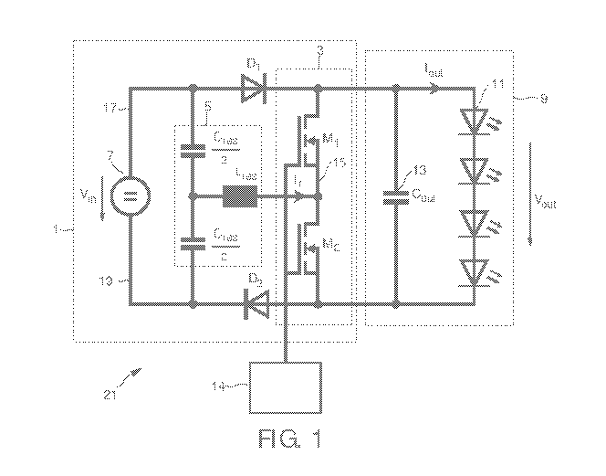
Fig. 1 shows a block diagram of a supply circuit 1 in accordance with an
embodiment of the present invention. The supply circuit 1 comprises a bridge
circuit 3, a
resonant circuit 5, which is coupleable at one end to a power source 7,
wherein the power
source 7 is preferably a direct voltage source V,,,. The supply circuit 1 is
coupled to a load
circuit 9, which comprises at least one, in Fig. 1 exemplary a total of four,
loads 11 and a
smoothing capacitor 13 being connected in parallel to the loads 11. A load 11
may be a LED,
an OLED or the like. The output voltage Voõ t is dropped across the array of
loads 11.
The bridge circuit 3 comprises at least two switches M1 and M2 that are
CA 02756020 2011-09-20
WO 2010/109371 PCT/IB2010/051109
exemplary MOSFETs, which are controlled by a control unit 14. In response to a
direct
current from the power source 7, the bridge circuit 3 communicates a voltage
signal to the
resonant circuit 5 at a switching frequency fsW,,,h, which in turn
communicates an alternating
current Ir to the load circuit 9.
5 The switches M1 and M2 of the bridge circuit 3 are preferably switched by
means of the control unit 14, which is adapted to provide a switching duty-
cycle of 50%.
Furthermore, the control unit 14 is adapted to provide a maximum switching
frequency fsW,,,n
of the bridge circuit 3, which is preferably half the resonant frequency fres
of the resonant
circuit 5.
The switches M1 and M2 are connected in series, whereas the source contact of
switch M1 is coupled to the drain contact of switch M2 by an interconnection
15.
The resonant circuit 5 is coupleable at one end to the power source 7 and
coupled at another end to the interconnection 15 of the at least two switches
M1 and M2 of the
bridge circuit 3. The resonant circuit 5 comprises an inductance Lres and a
capacitance Cres,
whereas the capacitance Cres is exemplary divided into two partial resonant
capacitances
Cres/2. Hence, each of the partial capacitances Cres/2 comprises half the
resonant capacitance
Cres.
Fig. 1 further illustrates that a diode D1 is assigned to the switch M1 and a
diode D2 is assigned to the switch M2. In particular, the diodes D1 and D2 are
interconnected
between each switch M1 and M2 and the power source 7 and are in particular
connected in
series with the respective assigned switch M1 or M2 on the one hand and to the
power source
7 on the other hand. One of the diodes, in particular diode D1 is polarized
with respect to the
assigned switch M1 so that a flow of negative (polarized) resonant current Ir
through diode D1
is allowed and another diode, in particular D2 is polarized with respect to
the assigned switch
M2 so that a flow of positive (polarized) resonant current Ir through diode D2
is allowed.
As will be explained in more detail later on, the voltage drop V1 across the
resonant circuit 5 depends on the diodes and depends in particular on which
diode is at present
conductive. Hence, the voltage drop across the resonant circuit 5 may be
summarized as fol-
lows: Ml on, Dl is conductive: -Vin/2; Ml connected to D2, D2 is conductive:
Vin/2 - Vout;
M2 connected to D2, D2 is conductive: Vin/2; M2 on, Dl is conductive: -Vin/2 +
Vout.
The partial capacitances Cres/2 are connected in series with the inductance
Lres
and further are coupled to the interconnections between a diode D1 or D2 and
the power
source 7. Thus, one partial capacitance Cres/2 is coupled to the
interconnection 17 between
diode D1 and the power source 7, and the other partial capacitance Cres/2 is
coupled to the
CA 02756020 2011-09-20
WO 2010/109371 PCT/IB2010/051109
6
interconnection 19 between diode D2 and the power source 7.
The above described novel topology of the supply circuit 1 realizes a DSRC-I
comprising most of its major advantages and in addition provides a boost
function, so that the
output voltage Vout is higher than the input voltage V,,, without the need for
any additional
components such as a transformer.
It shall be noticed that a device 21 according to the present invention
comprises that supply circuit 1 and may in addition comprise one or more load
circuits 9.
Fig. 2 shows a simulation schematic of the supply circuit 1 in accordance with
an embodiment of the present invention, whereas Fig. 3 to Fig. 6 show
simulation results for
different sets of parameter values. The simulation schematic of Fig. 2 is
based on the supply
circuit topology illustrated in Fig. 1
Fig. 3 shows simulation results for a second set of parameter values. In
particular, the simulation results are based on an input voltage V,,, = 24 V,
an output voltage
of Vout = 30 V and a switching frequency of the bridge circuit f witen = freS
/ 2, i.e., the
switching frequency is half the resonant frequency freS.
The topmost simulation schematic of Fig. 3 illustrates the currents I(V1) and
I(V4) as a function of time t. Thereby, the voltage V1 corresponds to the
voltage V,,,
illustrated in Fig. 1 and the voltage V2 corresponds to the voltage Vout
illustrated in Fig. 1. It
is obvious that the output current I(V4) is lower than the input current
I(V1).
The middle simulation schematic of Fig. 3 illustrates the diode currents I(D1)
and I(D4) as a function of time t. As explained above, that diodes D1 and D2
are connected to
their assigned switches M1 and M2 with opposite polarizations. Therefore, the
diodes D1 and
D2 allow current flow alternately depending on the polarization of the
resonant current Ir as
will be explained in more detail hereinafter.
The lower simulation schematic of Fig. 3 illustrates the resonant current
I(Lres)
as a function of time t. The resonant current I(LreS) corresponds to the
resonant current Ir of
Fig. 1.
Fig. 4 shows simulation results for a second set of parameter values. In
particular, the simulation results are based on an input voltage V,,, = 24 V,
an output voltage
of Vout = 40 V and a switching frequency of the bridge circuit fsW,tcn = fres
/ 2, i.e., the
switching frequency is half the resonant frequency freS.
Fig. 5 shows simulation results for a third set of parameter values. In
particular, the simulation results are based on an input voltage V,,, = 24 V,
an output voltage
of Vout = 50 V and a switching frequency of the bridge circuit fsW,tch = fres
/ 2, i.e., the
CA 02756020 2011-09-20
WO 2010/109371 PCT/IB2010/051109
7
switching frequency is half the resonant frequency freS.
Fig. 6 shows simulation results for a fourth set of parameter values. In
particular, the simulation results are based on an input voltage V,,, = 24 V,
an output voltage
of Vout = 40 V and a switching frequency of the bridge circuit twitch = freS /
3, i.e., the
switching frequency is one third of the resonant frequency freS.
In order to describe the functionality of the supply circuit 1, the topology
shown in Fig. 1 can be simplified as illustrated in Fig. 7 and Fig. 8. In Fig.
7, there are two
capacitances Cini and C,,,2 provided and additionally a resonant capacitance
Cres. In Fig. 8 the
partial resonant capacitances Cres/2 of Fig. 1 are combined to one single
capacitance Cres and
the power source 7 is virtually split into two partial power sources 7' and
7", each providing
a direct voltage V,,,/2. It should be noted that taking two partial
capacitances Cres or two
capacitances Cini and C,,,2 and in addition a resonant capacitance Cres leads
to the same result.
It can be seen from Fig. 8 that a voltage dropped across the capacitance Cres
is denoted as Vc
and a voltage dropped across the inductance Lres is denoted as VL.
The resonant circuit 5 can be described with its resonant frequency freS and
its
resonant impedance Zres.
fres /= (1)
27r Lres Cres
L
Zres = res (2)
Cres
Based on simulation results, the circuit behavior can be explained as follows:
For the
description in time intervals the half resonant period i is defined.
l=Tes=-= {~ (3)
2 2 J res
The switching period of the switches M1 and M2 is Tsitch as can be seen from
Fig. 7 and 2*Tres < Tswitch. The conducting parts in each time interval are
depicted in Fig. 10
to Fig. 13.
Fig. 9 shows a block diagram of the conducting parts of a supply circuit 1 in
accordance with an embodiment of the present invention for a first time
interval t1: 0 < t < i,
which is illustrated in Fig. 13. During this time interval, switch M1 is
switched on and switch
M2 is switched off. The resonant circuit 5 generates in this time interval a
first, negative
CA 02756020 2011-09-20
WO 2010/109371 PCT/IB2010/051109
8
sinusoidal half-wave exemplary denoted in Fig. 13 with Wi.
Hence, switch MI allows a current flow, which is communicated from the
direct voltage source 7'. The voltage dropped across the series resonant
circuit 3, i.e., across
capacitance Cres and inductance LreS is denoted in Fig. 9 with V1.
As the resulting current Jr is negative, the diode Di will be conductive for
this
current. Diode D2 is polarized opposed to diode Di and will therefore not
allow a flow of the
negative current Ir in the first time interval.
Based on simulation results, the conducting components in each time interval
are known and the amplitude of each sinusoidal half wave can be calculated.
From the
idealized circuit the voltage dropped across the resonant capacitor, denoted
in Fig. 8 as Vc(t),
at the beginning of the first time interval can be calculated. The result is:
Vc(t=0)=V0õt -Vin (4)
Additionally, the voltage drop Vi across Cres and LreS can be obtained from
Fig. 9:
With help of the initial condition and the voltage of the resonant capacitor
Vc, the amplitude
of each sinusoidal half-wave and the capacitor's voltage Vc after finishing
each cycle can be
calculated. For every cycle the voltage V1, applied to the whole resonant
circuit can be
obtained from the conducting parts. For the first cycle V, is:
V(0<t<-ti)=- Zn (5)
Based on idealized circuit behavior, the amplitude of the resulting first,
negative sinusoidal
half-wave WI can be calculated.
Vut + V"
2 (6)
h=
res
Z
Further current flow through Di after this half-wave is prevented by diode DI,
as current Ir
becomes positive.
Fig. 10 shows a block diagram of the conducting parts of a supply circuit 1 in
accordance with an embodiment of the present invention for a second time
interval t2:
i < t < Tsitch/2. During this time interval, switch MI is still switched on
and switch M2 is still
switched off. The resonant circuit 5 generates in this time interval a second,
positive
sinusoidal half-wave exemplary denoted in Fig. 13 with W2.
Hence, the current Ir is thus positive during this time interval t2.
Consequently,
CA 02756020 2011-09-20
WO 2010/109371 PCT/IB2010/051109
9
diode D1 does not allow current flow and thus blocks the positive current Ir.
However, diode
D2, which is polarized opposed to diode D2 allows current flow of the positive
current Jr. It is
obvious from Fig. 10 that the current lout flows through the output.
From calculations with formulas of the first time interval ti, the resonant
capacitors
voltage Vc(t) is:
VC (t=ti)=-Vout (7)
And Vi :
V, (c <t<-2ti)= Vn -Vout (8)
This leads to the amplitude of the second, positive sinusoidal half-wave W2:
Y in
2 (9)
j2 Z
res
Further current flow is prevented by diode D2.
Fig. 11 shows a block diagram of the conducting parts of the supply circuit 1
in accordance with an embodiment of the present invention for a third time
interval t3:
Tswitch/2 <t < Tswitch/2 + -c. During this time interval, switch M1 is
switched off and switch M2
is switched on. The resonant circuit 5 generates in this time interval a
third, positive
sinusoidal half-wave exemplary denoted in Fig. 13 with W3.
Hence, the current Ir is thus positive during this time interval t3.
Consequently,
diode D1 does not allow current flow and thus blocks the positive current Ir.
However, diode
D2, which is polarized opposed to diode D2 allows current flow of the positive
current Ir.
The behavior in the third and fourth time interval t3 and t4 is similar to
that of the first
one and second time interval ti and t2. Basically, the current half-waves
occur with the
opposite sign.
The capacitor voltage Vc(t) at the beginning of the third time period t3 is:
VC (t = switch / 2) Vi. - Vout (10)
And Vi :
Vl (Tswitch < t < Twitch +ti) = Vn ( 1 1
2 2 2 I
Consequently, the third, positive sinusoidal half-wave W3 has the following
amplitude:
CA 02756020 2011-09-20
WO 2010/109371 PCT/IB2010/051109
Vout Y In
13 2 (12) Z res
Fig. 12 shows a block diagram of the conducting parts of a supply circuit in
accordance with an embodiment of the present invention for a fourth time
interval t4:
Tswitah/2 + -c <t < Ts,itoh. During this time interval, switch M1 is still
switched off and switch
M2 is still switched on. The resonant circuit 5 generates in this time
interval a fourth, negative
5 sinusoidal half-wave exemplary denoted in Fig. 13 with W4.
Hence, the current Ir is thus negative during this time interval t4.
Consequently,
diode Dl does allow current flow of the negative current Ir. However, diode
D2, which is
polarized opposed to diode D2 does not allow current flow of the negative
current Ir. It is
obvious from Fig. 12 that the current Ires again flows through the output.
10 Finally, the capacitor voltage Vc(t) at the beginning of the fourth time
period
t4 is:
VC (t=Twitch /2+i)=Vout (13)
And V 1:
V! ! TT
(1 switch < t < 1 switch + 2,LI ) V-- + Vout (14)
Y 2 2 2
This leads to the amplitude of the fourth, negative, sinusoidal half-wave W4:
Yin
2 (15)
I4 = Z
res
The circuit behavior shows, that only two sinusoidal half-waves, namely W2
and W4 flow through the output. Consequently, the output current lout consists
of two
sinusoidal half-waves W2 and W4 per switching period T5,,itoh.
Hence, the average output current can be calculated to:
Y in
I 2 2T s = V;n'Tes (16)
out =
R Zres Twitch Zres Twitch
The functionality of the supply circuit 1 according to the invention and the
resulting "boost" function will now be explained in more detail: The topology
of the supply
CA 02756020 2011-09-20
WO 2010/109371 PCT/IB2010/051109
11
circuit 1 causes two of four half-waves (in particular every second of four
half-waves) of the
resonant current IreS not to flow through the output, i.e., the load. With
respect to Figs. 9 to
13, the first and the third half-waves W1 and W3 do not flow through the
output as can be
seen from Figs. 9 and 11.
This respective half-wave is e.g., I1 = (-Vout + V,,,/2) Zres, when referring
to the
first have wave W1 of Fig. 13. Taking into account the initial condition for
the voltage drop
across the capacitance Cres and the voltage drop V1 across the resonant
circuit 5, the amount
of the voltage drop across the capacitance Cres after the first half-wave W1
is equal to the
output voltage Vout. Hence, for the subsequent half-wave W2, the available
voltage is
resulting from the series connection of the voltage drop corresponding to Vout
across the
capacitance Cres and half of the input voltage V,,,/2.
However, the output voltage Vout always acts against the second half-wave
W2, and thus, the half of the input voltage, namely V,,,/2 is always left
over, enforcing a
current flow through the load. Consequently, the second and fourth half-waves
W2 and W4
flow through the load and the amplitude of the current is independent from the
load voltage
in case that the load voltage is larger than the input voltage V;,,.
Consequently, the present invention provides a supply circuit 1, in particular
a
converter topology that can be used for automotive LED/OLED lighting or in
general, for
battery powered LED/OLED lighting as it not only constitutes a DSRC-I, which
is preferably
used for the above-named applications, but due to the inventive topology, the
supply circuit 1
in addition provides a boost function providing a higher output voltage Vout
than the input
voltage Vi,, without the need for additional components. Above all, dimming of
LEDs/OLEDs
can be realized by decreasing the switching frequency f5W,teh. Waveforms with
decreased
switching frequency are shown in Fig. 6.
In a further embodiment, a control loop, i.e. a feedback loop, can be
additionally provided. The feedback loop would, for example, measure the LED
current or
voltage, send this signal to the controller and adjust the control signals of
the electronic
switches accordingly.
In summary, the novel topology of the supply circuit according to the present
invention offers basically the same major advantages as the conventional DSRC-
I converter,
but additionally it provides a higher output voltage Vout than the input
voltage V;,,.
Although the novel supply circuit may be considered to be disadvantageous
because of the conductive part over the two diodes D1 and D2 for an output
voltage Vout lower
than the input voltage V,,, in reality this will cause no problems, as the
forward threshold
CA 02756020 2011-09-20
WO 2010/109371 PCT/IB2010/051109
12
voltage of the connected load in particular LEDs result in a high output
voltage Vout. This
blocks current flow if the converter is not controlled.
Altogether, the converter provides the advantage that no current sensing and
current control is required, furthermore, a very compact circuit design is
provided with an
integrated voltage boost. The supply circuit according to the present
invention is above all
easy to design, simple to control and provides a high efficiency. It shall be
understood that
the same advantageous are valid for a device according to the invention,
comprising the
supply circuit.
While the invention has been illustrated and described in detail in the
drawings
and foregoing description, such illustration and description are to be
considered illustrative or
exemplary and not restrictive; the invention is not limited to the disclosed
embodiment. Other
variations to the disclosed embodiment can be understood and effected by those
skilled in the
art in practicing the claimed invention, from a study of the drawings, the
disclosure, and the
appended claims.
In the claims, the word "comprising" does not exclude other elements or steps,
and the indefinite article "a" or "an" does not exclude a plurality. A single
element or other
unit may fulfill the functions of several items recited in the claims. The
mere fact that certain
measures are recited in mutually different dependent claims does not indicate
that a
combination of these measured cannot be used to advantage.
Any reference signs in the claims should not be construed as limiting the
scope.