Note : Les descriptions sont présentées dans la langue officielle dans laquelle elles ont été soumises.
CA 02757818 2011-09-30
WO 2010/151400
PCT/US2010/036980
FET WITH REPLACEMENT GATE STRUCTURE AND METHOD OF
FABRICATING THE SAME
FIELD OF THE INVENTION
[0001] The invention relates to a replacement gate structure for a field
effect transistor
(FET) and method of manufacturing, and more particularly, to a multi-gate FET
replacement gate structure and method of fabricating the multi-gate FET
replacement
gate structure.
BACKGROUND
[0002] A Multi-gate FET (MUGFET) is a family of MOSFETs in which more than one
gate contact is used to control output current. MUGFETs are known to have
superior
gate control of the channel compare to single gate MOSFETs. For example, in a
multigate device, the channel is surrounded by several gates on multiple
surfaces,
allowing more effective suppression of "off-state" leakage current. Multiple
gates also
allow enhanced current in the "on" state, known as drive current. These
advantages
translate to lower power consumption and enhanced device performance.
[0003] MUGFETs are one of several strategies developed to create ever-smaller
microprocessors and memory cells, for example. In fact, many manufactures
predict that
MUGFET technologies will be the cornerstone of sub-32 nm technologies. The
primary
roadblock, however, to widespread implementation is manufacturability, as both
planar
and non-planar designs present processing challenges. These challenges may
include
lithography and patterning processes, as well as resultant high parasitic S/D
resistance.
[0004] MUGFETs come in a variety of different architectures. For example,
MUGFETs may be planar or non-planar devices. However, at sizes of, for
example, 32
CA 02757818 2011-09-30
WO 2010/151400
PCT/US2010/036980
nm, planar transistors are expected to suffer from undesirable short channel
effects,
especially "off-state" leakage current. These off state leakage currents will
increase the
idle power required by the device. Nonplanar devices, on the other hand, are
more
compact than conventional planar transistors, enabling higher transistor
density which
translates to smaller overall microelectronics. But, a challenge to integrate
non planar
MUGFETs into conventional semiconductor manufacturing processes include, for
example, fabrication of a thin silicon "fin" and of matched gates on multiple
sides of the
fin. Also, in conventional MUGFET devices, there is a large capacitance
between the
fins, which may result in decreased performance characteristics.
[0005] Accordingly, there exists a need in the art to overcome the
deficiencies and
limitations described hereinabove.
SUMMARY
[0006] In an aspect of the invention, a method of manufacturing a structure
comprises
forming temporary spacer gates about a plurality of active regions and
depositing a
dielectric material over the temporary spacer gates, including between the
plurality of
active regions. The method further includes etching portions of the dielectric
material to
expose the temporary spacer gates and removing the temporary spacer gates,
leaving a
space between the active regions and a remaining portion of the dielectric
material. The
method additionally includes filling the space between the active regions and
above the
remaining portion of the dielectric material with a gate material.
[0007] In an aspect of the invention, a method of manufacturing a MUGFET,
comprises: forming a plurality of active regions on a substrate; forming a
sacrificial
spacer gate about each of the active regions; depositing a dielectric material
over the
sacrificial spacer gate; over etching the dielectric material to form an
opening in the
2
CA 02757818 2011-09-30
WO 2010/151400
PCT/US2010/036980
dielectric material and to expose the sacrificial spacer gate; etching the
sacrificial spacer
gate to form spaces between each of the plurality of active regions and the
dielectric
material which remains between each of the plurality of active regions after
the over
etching; and depositing gate material in the spaces and the opening.
[0008] In an aspect of the invention, a MUGFET structure comprises a dual
damascene
replacement gate structure having a lower portion and an upper portion. The
lower
portion has a gate thickness of about 30% or less of a distance between
adjacent active
devices and the upper portion straps the adjacent active devices.
[0009] In another aspect of the invention, a design structure embodied in a
machine
readable medium for designing, manufacturing, or testing an integrated circuit
is
provided. The design structure comprises the structures and/or methods of the
present
invention.
BRIEF DESCRIPTION OF THE SEVERAL VIEWS OF THE DRAWINGS
[0010] The present invention is described in the detailed description which
follows, in
reference to the noted plurality of drawings by way of non-limiting examples
of
exemplary embodiments of the present invention.
[0011] FIGS. 1-6 show intermediate structures and respective processing steps
in
accordance with aspects of the invention;
[0012] FIG. 7 shows a final structure and respective processing steps in
accordance
with aspects of the invention; and
[0013] FIG. 8 is a flow diagram of a design process used in semiconductor
design,
manufacture, and/or test.
3
CA 02757818 2011-09-30
WO 2010/151400
PCT/US2010/036980
DETAILED DESCRIPTION
[0014] The invention relates to a replacement gate structure for a field
effect transistor
(FET) and method of manufacturing, and more particularly, to a multi-gate FET
(MUGFET) replacement gate structure and method of fabricating the MUGFET
replacement gate structure. In implementation, the method of manufacture
includes a
dual damascene MUGFET replacement gate. Advantageously, the method of forming
the structures allows the gate to gate strapping of adjacent fins of a MUGFET,
while
reducing gate to source/drain (S/D) capacitance. Also, the structure of the
present
invention has a lower capacitance with the source/drain region than
conventional
devices. The present invention also results in a structure that is non-planar
and which
straddles the fins of the MUGFET.
[0015] FIG. 1 shows a beginning structure in accordance with aspects of the
invention.
In particular, FIG. 1 shows a plurality of active regions 12 formed on a BOX
such as, for
example, an SOI layer 10. The active regions 12 can be, for example, fins for
a
MUGFET. The active regions 12 can be formed in a conventional manner known to
those of skill in the art. For example, the fins (active regions 12) can be
formed by a
conventional masking and etching process, as should be understood by those of
skill in
the art such that further explanation is not required herein.
[0016] The active regions 12 have an aspect ratio, in embodiments, of about
1.5; that
is, the height of the active region is about 1.5 times the width of the active
region. It
should be understood, though, that other aspect ratios are also contemplated
by the
present invention, and that an aspect ratio of 1.5 should not be considered a
limiting
feature of the present invention. The spacing between adjacent active regions
12 can be
4
CA 02757818 2011-09-30
WO 2010/151400
PCT/US2010/036980
about 2 to 3 times the width of the active region 12. For example, for a 20 nm
node, the
space between the adjacent active regions can be about 40nm to 60 nm. Again,
it should
be understood that other distances are also contemplated by the present
invention, and
that the present invention should not be limited by the space between the
adjacent active
regions.
[0017] FIG. 2 shows an optional processing step in accordance with aspects of
the
invention. In particular, FIG. 2 shows the formation of a dielectric and metal
region 14
surrounding the active regions 12. The dielectric material can be, for
example, any
suitable dielectric material such as SiO2, SiON, Hafnium, Zirconium, etc. The
metal can
be any suitable metal such as, for example, TaN or TiN, to name a few metals.
In
embodiments, the dielectric and metal region 14 is formed using a conventional
deposition and etching process. For example, the dielectric and metal region
14 can be
formed by a conventional Atomic Layer Deposition (ALD) and a subsequent
etching of
excess material on the SOI layer 10.
[0018] In FIG. 3, a temporary spacer gate 16 (sacrificial gate) is formed to
surround the
active region 12. The temporary spacer gate 16 will act as a spacer gate,
which will
subsequently be removed to provide a space between the active region 12 and a
dielectric
material. This will effectively lower the capacitance of the final structure.
In
embodiments, the temporary gate 16 is a polysilicon material that is deposited
directly
over and in contact with either the active regions 12 or the dielectric and
metal regions
14, depending on the implementation of the processes discussed in FIG. 2. The
spacer
gate 16 is etched to remove material from the source/drain region.
[0019] In embodiments, the sidewall thickness of the spacer gate 16 is about
10 nm to
about 20 nm for a spacing of about 60 nm between adjacent active regions 12.
In further
CA 02757818 2011-09-30
WO 2010/151400
PCT/US2010/036980
embodiments, the spacer gate 16 can be other dimensions such as, for example,
5nm to
about 30 nm. In embodiments, though, the sidewall thickness (and distance
between
active regions) can vary so long as a space remains between the active region
12 and a
dielectric material, as discussed in more detail below. For example, in one
contemplated
embodiment, the thickness of the sidewall may be about one third (1/3) or less
of the
spacing between adjacent active regions 12.
[0020] FIG. 4 shows a deposition of dielectric material on the structure of
FIG. 3. In
particular, using a conventional deposition process such as, for example, CVD,
a
dielectric material 18 is deposited on the structures shown in FIG. 3. The
dielectric
material 18 may be any appropriate dielectric material such as, for example,
SiO2.
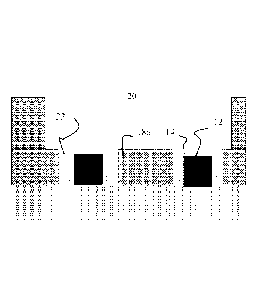
[0021] FIG. 5 shows an etching process in accordance with the present
invention.
More specifically, the dielectric material 18 is etched to form an opening 20
which
exposes the temporary spacer gates 16. That is, in embodiments, the dielectric
material
18 is etched to expose at least the top of the temporary spacer gates16. In
embodiments,
the dielectric material 18 can also be over etched to expose the sidewalls of
the
temporary spacer gates 16. The etching process can be accomplished using any
conventional etchant and etching process appropriate for the dielectric
material 18. For
example, in one conventional process, a mask (not shown) is applied on the
dielectric
material 18, which is opened using a conventional lithographic process. The
dielectric
material 18 is then etched through the opening, to the temporary spacer gates
16.
[0022] In FIG. 6, the temporary spacer gates 16 are removed using a
conventional
etching process. More specifically, the temporary spacer gates 16 are removed
to form a
space 22 between the remaining dielectric material 18a and the adjacent active
regions
12 (or dielectric and metal region 14). The temporary spacer gates 16 can be
removed
6
CA 02757818 2011-09-30
WO 2010/151400
PCT/US2010/036980
using an etchant that is selective to the material of the temporary spacer
gate, e.g.,
selective to polysilicon. After removal of the temporary spacer gates,
dielectric material
18a remains between adjacent active regions 12 (or dielectric and metal region
14) with
the space 22 provided between the dielectric material 18a and each of the
active regions
12.
[0023] In embodiments, the etching results in the formation of the space 22
(cavity),
which can range from about 10 nm to about 20 nm for a 60 nm spacing between
adjacent
active regions 12. In embodiments, though, the space 22 can be a different
dimension so
long as a space remains between the active regions 12 and the dielectric
material 18. For
example, in one contemplated embodiment, the space 22 can be about one third
(1/3) or
less than the spacing between adjacent active regions 12.
[0024] FIG. 7 shows a final structure and respective processing steps in
accordance
with the invention. Specifically, after the temporary spacer gates are
removed, a
replacement gate 24 is deposited in the etched area, e.g., in the space 22 and
space 20.
The replacement gate 24 can be deposited using a dual damascene deposition
process.
The replacement gate 24 can be planarized to form a polished flat surface 24a.
In
embodiments, the replacement gate 24 can be, for example, any appropriate
metal
depending on the desired work function.
[0025] In the structure thus described, the replacement gate 24 straddles
(straps) the
active regions (fins) 12, with the dielectric material 18a there between.
Advantageously,
the dielectric material 18a, i.e., non-gate material, located between the
active regions 12
will lower the capacitance of the device. Also, as the device is tunable,
e.g., the spacing
can vary (e.g., sidewall thickness of the temporary spacer gate can be
adjusted), such that
the device can have a capacitance depending on the desired characteristics of
the device.
7
CA 02757818 2011-09-30
WO 2010/151400
PCT/US2010/036980
DESIGN STRUCTURE
[0026] FIG. 8 illustrates multiple such design structures including an input
design
structure 920 that is preferably processed by a design process 910. Design
structure 920
may be a logical simulation design structure generated and processed by design
process
910 to produce a logically equivalent functional representation of a hardware
device.
Design structure 920 may also or alternatively comprise data and/or program
instructions
that when processed by design process 910, generate a functional
representation of the
physical structure of a hardware device. Whether representing functional
and/or
structural design features, design structure 920 may be generated using
electronic
computer-aided design (ECAD) such as implemented by a core developer/designer.
When encoded on a machine-readable data transmission, gate array, or storage
medium,
design structure 920 may be accessed and processed by one or more hardware
and/or
software modules within design process 910 to simulate or otherwise
functionally
represent an electronic component, circuit, electronic or logic module,
apparatus, device,
or system such as those shown in FIGS. 1-7. As such, design structure 920 may
comprise files or other data structures including human and/or machine-
readable source
code, compiled structures, and computer-executable code structures that when
processed
by a design or simulation data processing system, functionally simulate or
otherwise
represent circuits or other levels of hardware logic design. Such data
structures may
include hardware-description language (HDL) design entities or other data
structures
conforming to and/or compatible with lower-level HDL design languages such as
Verilog and VHDL, and/or higher level design languages such as C or C++.
[0027] Design process 910 preferably employs and incorporates hardware and/or
software modules for synthesizing, translating, or otherwise processing a
8
CA 02757818 2011-09-30
WO 2010/151400
PCT/US2010/036980
design/simulation functional equivalent of the components, circuits, devices,
or logic
structures shown in FIGS. 1-7 to generate a netlist 980 which may contain
design
structures such as design structure 920. Netlist 980 may comprise, for
example,
compiled or otherwise processed data structures representing a list of wires,
discrete
components, logic gates, control circuits, I/O devices, models, etc. that
describes the
connections to other elements and circuits in an integrated circuit design.
Netlist 980
may be synthesized using an iterative process in which netlist 980 is
resynthesized one or
more times depending on design specifications and parameters for the device.
As with
other design structure types described herein, netlist 980 may be recorded on
a machine-
readable data storage medium or programmed into a programmable gate array. The
medium may be a non-volatile storage medium such as a magnetic or optical disk
drive,
a programmable gate array, a compact flash, or other flash memory.
Additionally, or in
the alternative, the medium may be a system or cache memory, buffer space, or
electrically or optically conductive devices and materials on which data
packets may be
transmitted and intermediately stored via the Internet, or other networking
suitable
means.
[0028] Design process 910 may include hardware and software modules for
processing
a variety of input data structure types including netlist 980. Such data
structure types
may reside, for example, within library elements 930 and include a set of
commonly
used elements, circuits, and devices, including models, layouts, and symbolic
representations, for a given manufacturing technology (e.g., different
technology nodes,
32nm, 45 nm, 90 nm, etc.). The data structure types may further include design
specifications 940, characterization data 950, verification data 960, design
rules 970, and
test data files 985 which may include input test patterns, output test
results, and other
testing information. Design process 910 may further include, for example,
standard
9
CA 02757818 2011-09-30
WO 2010/151400
PCT/US2010/036980
mechanical design processes such as stress analysis, thermal analysis,
mechanical event
simulation, process simulation for operations such as casting, molding, and
die press
forming, etc. One of ordinary skill in the art of mechanical design can
appreciate the
extent of possible mechanical design tools and applications used in design
process 910
without deviating from the scope and spirit of the invention. Design process
910 may
also include modules for performing standard circuit design processes such as
timing
analysis, verification, design rule checking, place and route operations, etc.
[0029] Design process 910 employs and incorporates logic and physical design
tools
such as HDL compilers and simulation model build tools to process design
structure 920
together with some or all of the depicted supporting data structures along
with any
additional mechanical design or data (if applicable), to generate a second
design structure
990. Design structure 990 resides on a storage medium or programmable gate
array in a
data format used for the exchange of data of mechanical devices and structures
(e.g.
information stored in a IGES, DXF, Parasolid XT, JT, DRG, or any other
suitable format
for storing or rendering such mechanical design structures). Similar to design
structure
920, design structure 990 preferably comprises one or more files, data
structures, or other
computer-encoded data or instructions that reside on transmission or data
storage media
and that when processed by an ECAD system generate a logically or otherwise
functionally equivalent form of one or more of the embodiments of the
invention shown
in FIGS. 1-7. In one embodiment, design structure 990 may comprise a compiled,
executable HDL simulation model that functionally simulates the devices shown
in
FIGS. 1-7.
[0030] Design structure 990 may also employ a data format used for the
exchange of
layout data of integrated circuits and/or symbolic data format (e.g.
information stored in
CA 02757818 2011-09-30
WO 2010/151400
PCT/US2010/036980
a GDSII (GDS2), GL1, OASIS, map files, or any other suitable format for
storing such
design data structures). Design structure 990 may comprise information such
as, for
example, symbolic data, map files, test data files, design content files,
manufacturing
data, layout parameters, wires, levels of metal, vias, shapes, data for
routing through the
manufacturing line, and any other data required by a manufacturer or other
designer/developer to produce a device or structure as described above and
shown in
FIGS. 1-7. Design structure 990 may then proceed to a stage 995 where, for
example,
design structure 990: proceeds to tape-out, is released to manufacturing, is
released to a
mask house, is sent to another design house, is sent back to the customer,
etc.
[0031] The methods as described above is used in the fabrication of integrated
circuit
chips. The resulting integrated circuit chips can be distributed by the
fabricator in raw
wafer form (that is, as a single wafer that has multiple unpackaged chips), as
a bare die,
or in a packaged form. In the latter case the chip is mounted in a single chip
package
(such as a plastic carrier, with leads that are affixed to a motherboard or
other higher
level carrier) or in a multichip package (such as a ceramic carrier that has
either or both
surface interconnections or buried interconnections). In any case the chip is
then
integrated with other chips, discrete circuit elements, and/or other signal
processing
devices as part of either (a) an intermediate product, such as a motherboard,
or (b) an end
product. The end product can be any product that includes integrated circuit
chips.
[0032] The terminology used herein is for the purpose of describing particular
embodiments only and is not intended to be limiting of the invention. As used
herein, the
singular forms "a", "an" and "the" are intended to include the plural forms as
well, unless
the context clearly indicates otherwise. It will be further understood that
the terms
"comprises" and/or "comprising," when used in this specification, specify the
presence of
11
CA 02757818 2011-09-30
WO 2010/151400
PCT/US2010/036980
stated features, integers, steps, operations, elements, and/or components, but
do not
preclude the presence or addition of one or more other features, integers,
steps,
operations, elements, components, and/or groups thereof
[0033] The corresponding structures, materials, acts, and equivalents of all
means or
step plus function elements, if any, in the claims below are intended to
include any
structure, material, or act for performing the function in combination with
other claimed
elements as specifically claimed. The description of the present invention has
been
presented for purposes of illustration and description, but is not intended to
be exhaustive
or limited to the invention in the form disclosed. Many modifications and
variations will
be apparent to those of ordinary skill in the art without departing from the
scope and
spirit of the invention. The embodiments were chosen and described in order to
best
explain the principles of the invention and the practical application, and to
enable others
of ordinary skill in the art to understand the invention for various
embodiments with
various modifications as are suited to the particular use contemplated.
12