Note : Les descriptions sont présentées dans la langue officielle dans laquelle elles ont été soumises.
CA 02757995 2011-10-06
WO 2010/118317 PCT/US2010/030537
Attorney Docket No. 49256-111839
INTEGRATED TOUCH SENSOR ELECTRODE AND BACKLIGHT MASK
CROSS-REFERENCE TO RELATED APPLICATIONS
[0001] This application claims priority from and incorporates by reference the
disclosure
of United States Provisional Patent Application No. 61/168,152, filed on April
9, 2009.
BACKGROUND OF THE INVENTION
[0002] Controlled devices, for example, automobiles, home appliances, consumer
electronics, industrial machinery, and the like, can include one or more local
or remote user
interfaces through which a user can interact with the device. Such user
interfaces can include
displays providing information about the device and switching means that can
be actuated by a
user to control the device or a function thereof. Such switching means often
are embodied as
electronic sensors, for example, field effect sensors or capacitive sensors.
Such sensors typically
include one or more sensing electrodes and control circuitry for operating the
sensors.
[0003] User interfaces using such electronic sensors (sometimes referred to
herein as
touch sensors) can include a user interface substrate having one or more
operable touch surfaces
through which the user interacts with the controlled device and a touch sensor
substrate bearing
one or more corresponding touch sensors attached to the user interface panel.
Such user
interface substrates can be embodied as glass or plastic panels, and such
touch sensor substrates
can be embodied as printed wiring boards or flexible circuit carriers attached
to a surface of the
user interface substrate.
[0004] Such touch sensor substrates can bear a number of touch sensors, each
including
one or more sensing electrodes. Such user interface substrates can include
some form of indicia,
1
CA 02757995 2011-10-06
WO 2010/118317 PCT/US2010/030537
Attorney Docket No. 49256-111839
for example, words or symbols, in proximity to each touch sensor for
identifying the touch
sensor's location and/or function. The indicia can overlie the respective
touch sensors' sensing
electrode(s), thereby positively identifying their locations. The indicia can
be etched, screened,
printed, or otherwise formed or disposed on the user interface substrate.
[0005] Such user interfaces can include backlighting that illuminates selected
portions of
the user interface panel, for example, the indicia identifying the various
touch sensors, using a
light source located behind the user interface substrate. Some user interfaces
use backlighting
and backlight masks (typically in the form of dark frit or decorative ink on
the user interface
substrate), instead of (or in addition to) decoration on the user interface
substrate to define the
indicia. In such embodiments, the indicia typically appear as illuminated
portions of the user
interface substrate (provided by the backlighting) against a dark background
(provided by the
backlight mask). Alternatively, the indicia can appear to the user as dark
portions of the user
interface substrate (provided by the backlight mask) against an illuminated
background
(provided by the backlighting).
[0006] Frit and decorative ink typically are not completely opaque. As such,
backlight
masks made of frit and/or decorative ink can allow some light to bleed there
through and thereby
into and through portions of the user interface substrate that are intended to
appear opaque. As
such, the contrast between the indicia and the background can be less than
ideal, with the indicia
appearing less distinctly than desired, particularly when the indicia are
relatively small.
BRIEF DESCRIPTION OF THE DRAWINGS
[0007] Fig. 1 is a plan view of an illustrative embodiment of a user interface
substrate 12
showing a user interface substrate 12 as it might be viewed by a user, which
user interface
2
CA 02757995 2011-10-06
WO 2010/118317 PCT/US2010/030537
Attorney Docket No. 49256-111839
substrate 12 defines operative touch surfaces 14 corresponding to touch
sensors 16 associated
with the other side of user interface substrate 12 and which also defines
areas corresponding to
indicators 18 and indicia 20;
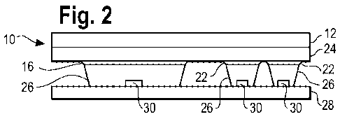
[0008] Fig. 2 is a cross-sectional side view of an illustrative embodiment of
a user
interface 10 including user interface substrate 12, circuit carrier 24
associated with the rear
surface of user interface substrate 12, touch sensor sensing electrodes 16 and
masks 22 disposed
on a rear surface of circuit carrier 24, and lighting substrate 28, light
sources 30, and light guides
26 associated with circuit carrier 24, sensing electrodes 16 and masks 22;
[0009] Fig. 3 is a cross-sectional side view of another illustrative
embodiment of a user
interface 10 including user interface substrate 12, circuit carrier 24
associated with the rear
surface of user interface substrate 12, touch sensor sensing electrodes 16 and
masks 22 disposed
on a front surface of circuit carrier 24, and lighting substrate 28, light
sources 30, and light
guides 26 associated with circuit carrier 24, sensing electrodes 16 and masks
22;
[0010] Fig. 4 is a cross-sectional side view of yet another illustrative
embodiment of a
user interface 10 including user interface substrate 12, circuit carrier 24
associated with the rear
surface of user interface substrate 12, touch sensor sensing electrodes 16 and
masks 22 disposed
on a front surface of circuit carrier 24, and light sources 30 and reflectors
32 associated with
circuit carrier 24, sensing electrodes 16 and masks 22; and
[0011] Fig. 5 is a plan view of a rear surface of a circuit carrier 24 bearing
touch sensor
sensing electrodes 16, masks 22, electrical traces 34, and bonding pads 36.
3
CA 02757995 2011-10-06
WO 2010/118317 PCT/US2010/030537
Attorney Docket No. 49256-111839
DETAILED DESCRIPTION OF THE ILLUSTRATED EMBODIMENTS
[0012] Fig. 1 illustrates an embodiment of a user interface 10 as it might
appear to a user.
More particularly, Fig. 1 shows a front or other user-oriented surface of a
user interface substrate
12 defining touch surfaces 14. Touch surfaces 14 correspond, respectively, to
touch sensor
sensing electrodes 16 (shown in phantom) associated with the other side of
user interface
substrate 12. Each sensing electrode 16 can form a portion of a corresponding
touch sensor that
can be actuated by touch or proximity of a stimulus, for example, a user's
finger or other object,
to the respective touch surface 14, as would be understood by one skilled in
the art and as
discussed further below.
[0013] Fig. 1 shows indicia in the form of the words "START" and "STOP" in the
areas
of user interface surface 12 corresponding to touch surfaces 14. These indicia
are defined by
light-transmissive portions, for example, apertures, in corresponding sensing
electrodes 16
associated with the other side of user interface surface 12. These indicia can
be selectively
illuminated by backlighting, as discussed further below. These indicia can,
but need not, be
generally visible to a user when the corresponding backlighting is not
energized. For example,
with the corresponding backlighting de-energized, the indicia could appear
dark, opaque or
otherwise generally take on the appearance of surrounding portions of the
surface of user
interface substrate 12.
[0014] User interface 10 also includes indicators 18 and corresponding indicia
20, both
of which are visible from the front surface of user interface substrate 12.
Indicator 18 and indicia
20 are defined by corresponding masks 22 (shown in phantom) associated with
the other side of
user interface substrate 12. Indicators 18 and/or indicia 20 can be
selectively illuminated by
backlighting, as discussed further below. Indicators 18 and/or indicia 20 can,
but need not be,
4
CA 02757995 2011-10-06
WO 2010/118317 PCT/US2010/030537
Attorney Docket No. 49256-111839
generally visible to a user when the corresponding backlighting is not
energized. For example,
with the corresponding backlighting de-energized, indicators 18 and/or indicia
20 can appear
dark, opaque or otherwise generally take on the appearance of surrounding
portions of the
surface of user interface substrate 12.
[0015] The forms of touch surfaces 14 as shown in the drawings are merely
illustrative.
In other embodiments, touch surfaces could take other forms, for example,
round or square, and
they could be located elsewhere with respect to user interface substrate 12,
indicators 18 and
indicia 20. Similarly, the forms of indicia 20 and the indicia corresponding
to surfaces 14 as
shown in the drawings are merely illustrative. In other embodiments, these
indicia could take
other forms, for example, one or more other words, letters, numbers, or
symbols. Alternatively,
the indicia could be omitted. Likewise, the forms of indicators 18 shown in
the drawings are
merely illustrative. In other embodiments, indicators 18 could be of other
sizes and shapes, and
they could be located elsewhere with respect to indicia 20. Alternatively,
indicators 18 could be
omitted.
[0016] Fig. 2 illustrates an embodiment of a user interface 10 in cross-
section. More
particularly, Fig. 2 shows user interface substrate 12, circuit carrier 24
associated with the rear
surface of user interface substrate 12, and sensing electrodes 16 and masks 22
disposed on the
rear surface of circuit carrier 24. Fig. 2 also shows a lighting substrate 28
bearing light sources
30 and light guides 26 optically coupling light sources 30 to corresponding
ones of sensing
electrodes 16 and masks 22.
[0017] User interface substrate 12 could be made of any suitable material, for
example,
glass or plastic, as would be recognized by one skilled in the art. At least
the portions of user
interface substrate 12 corresponding to indicators 18, indicia 20, and the
indicia corresponding to
CA 02757995 2011-10-06
WO 2010/118317 PCT/US2010/030537
Attorney Docket No. 49256-111839
touch surfaces 14 should be sufficiently transparent or translucent to allow
light from light
sources 30 to be visible at the user-oriented surface of user interface
substrate 12. Other portions
of user interface substrate 12 could, but need not, be generally opaque or
otherwise not generally
transparent or translucent, or they could be rendered as such by means of dark
ink, frit, or an
overlay having generally opaque or non-light-transmissive portions (not shown)
applied to either
surface thereof. Preferably, the user-oriented surface of user interface
substrate 12 has a dead
front or dark appearance that provides substantial contrast to the light
emanating from associated
backlight units, as will be discussed further below.
[0018] Circuit carrier 24 could be any suitable form of rigid or flexible
circuit carrier, as
would be recognized by one skilled in the art. For example, circuit carrier 24
could be embodied
as a rigid substrate, such as a printed wiring board made of FR4 or other
suitable material. In
other embodiments, circuit carrier 24 could be a flexible circuit carrier made
of polyester or other
suitable material. Portions of circuit carrier 24 corresponding to sensor
electrodes 16 and masks
22 (or, more particularly, the apertures or otherwise light-transmissive
portions thereof) should
be transparent, translucent or otherwise sufficiently light-transmissive to
allow light from light
sources 30 to pass there through. Other portions of circuit carrier 24 could,
but need not, be
similarly light transmissive. Alternatively, such other portions could be
generally opaque or
rendered as such by a coating, overlay, or otherwise.
[0019] Circuit carrier 24 could be attached to user interface substrate 12 in
any suitable
manner. For example, circuit carrier 24 could be attached to user interface
substrate 12 using
adhesives, mechanical fasteners, snap-fit structures, and/or other means, as
would be recognized
by one skilled in the art.
6
CA 02757995 2011-10-06
WO 2010/118317 PCT/US2010/030537
Attorney Docket No. 49256-111839
[0020] As illustrated in Fig. 5, sensing electrodes 16 include apertures 38
through which
light can pass. Apertures 38 collectively correspond to and define the indicia
visible at the front
surface of user interface substrate 12 in the regions of touch surfaces 14.
Similarly, masks 22
include apertures 38 defining indicators 18 and indicia 20. Figs. 1 and 5
depict sensing
electrodes 16 and masks 22 as generally rectangular. In other embodiments,
sensing electrodes
16 and masks 22 can be square, round, or have any other regular or irregular
shape.
[0021] Preferably, sensing electrodes 16 and masks 22 are made of a
substantially
opaque material. In other embodiments, sensing electrodes 16 and masks 22
could be made of
material that is less than substantially opaque, that is, material that is
somewhat light
transmissive. In certain embodiments, sensing electrodes 16 could be made of a
substantially
opaque conductive material defining apertures 38 therein, and could further
include a
substantially transparent conductive material (not shown) at least in the area
of apertures 38, that
is, superimposed with apertures 38. Such a substantially transparent
conductive material could
be disposed upon or underneath, and be electrically coupled to, the
substantially opaque
conductive material. Such transparent conductive material could effectively
increase the surface
area of sensing electrodes 16 and potentially improve their performance, while
not adversely
affecting their ability to transmit light through apertures 38 and thereby
define the indicia to be
visible at touch surfaces 14.
[0022] Sensing electrodes 16 could be disposed on circuit carrier 24 in any
suitable
manner. For example, circuit carrier 24 could be plated or otherwise coated
with conductive
material, such as copper or aluminum, and then patterned and etched to yield
sensing electrodes
16 and masks 22. Such conductive material also could be patterned and etched
to form other
circuitry, including without limitation electrical traces 34 and bonding pads
36 that might be
7
CA 02757995 2011-10-06
WO 2010/118317 PCT/US2010/030537
Attorney Docket No. 49256-111839
needed for the construction and operation of touch sensors associated with
sensing electrodes 16
and/or other elements of user interface 10. Alternatively, sensing electrodes
16, masks 22 and/or
additional circuitry could be disposed on circuit carrier 24 by sputtering,
application of
conductive ink, or other techniques, as would be recognized by one skilled in
the art. In other
embodiments, masks 22 could be made of any suitable non-conductive material
applied to circuit
carrier 24 in any suitable manner.
[0023] Sensing electrodes 16 could form part of any suitable type of touch
sensor that
can be actuated by proximity or touch of a user's finger or other object, as
would be recognized
by one skilled in the art. For example, sensing electrodes 16 could be coupled
to a TS-100 AS IC
available from TouchSensor Technologies, LLC of Wheaton, IL to form a touch
sensor as
described in U.S. Patent No. 6,320,282 and related patents and applications.
Alternatively,
sensing electrodes 16 could be coupled to control circuitry to form touch
sensors such as those
disclosed in U.S. Patent Nos. 5,594,222 and 6,310,611. U.S. Patent Nos.
5,594,222 and
6,320,282 disclose touch sensors having active components in close proximity
to one or more
sensing electrodes. In other embodiments, sensing electrodes 16 could be
coupled to control
circuitry to form capacitive touch sensors as would be recognized by one
skilled in the art. In
any of the foregoing embodiments, the touch sensor control circuitry could be
disposed on the
same (or other) side of the same carrier or substrate as sensing electrodes 16
and/or masks 22.
[0024] Sensing electrodes 16 and masks 22 are shown in the drawings as being
disposed
on circuit carrier 24, which in turn is attached to user interface substrate
12. Alternatively,
sensing electrodes 16 and/or masks 22 could be at least partially embedded
within circuit carrier
24. In other embodiments, sensing electrodes 16 and/or masks 22 could be
disposed directly
onto user interface substrate 12 or at least partially embedded within user
interface substrate 12.
8
CA 02757995 2011-10-06
WO 2010/118317 PCT/US2010/030537
Attorney Docket No. 49256-111839
In such embodiments, additional circuitry that might be used for the
construction or operation of
touch sensors corresponding to sensing electrodes 16 or other portions of user
interface 10 also
could be similarly disposed on user interface substrate 12 and circuit carrier
24 could be omitted.
Alternatively circuit carrier 24 could be retained to, for example, carry
other circuitry, lighting
elements or the like. In further embodiments, touch surfaces 14 could be
defined by circuit
carrier 24 or an overlay (for example, a decorative overlay) thereon. In such
embodiments,
circuit carrier 24 could function as a user interface substrate, and user
interface substrate 12
could be omitted as a separate structure.
[0025] Masks 22 are shown in the drawings as defining apertures 38
corresponding to
both indicators 18 and indicia 20. In other embodiments, individual masks 22
could be used to
define indicators 18 and indicia 20.
[0026] Lighting substrate 28 can be made of any suitable material and can be
attached to,
for example, circuit carrier 24 or user interface substrate 12 by any suitable
means, including
adhesives, snap-fit structures, stand-offs, mechanical fasteners, and the
like, as would be
recognized by one skilled in the art. Light guides 26 can be integral with
lighting substrate 28 or
they can be discrete components attached to lighting substrate 28. Light
sources 30 can be any
suitable form of light source, for example, LEDs, lamps, and the like, as
would be recognized by
one skilled in the art. Light sources 30 can be disposed on and powered from
lighting substrate
28.
[0027] Preferably, light guides 26 abut circuit carrier 24 and/or sensing
electrodes 16 and
masks 22 thereon and/or intermediate, substantially light-tight gaskets (not
shown) so as to
substantially direct/contain light emanating from corresponding light source
30 to the respective
electrode 16 or mask 22 and preclude spread of light emanating from such light
source 30 to
9
CA 02757995 2011-10-06
WO 2010/118317 PCT/US2010/030537
Attorney Docket No. 49256-111839
surrounding regions of circuit carrier 24, user interface substrate 12, and/or
the environment
generally. Light guides could be made of any suitable material, for example,
an inherently
reflective material. In other embodiments, light guides 26 could be coated
with a reflective
material.
[0028] Fig. 3 is side view of another embodiment of user interface 10. This
embodiment
is similar to the Figs. 1 and 2 embodiment but differs in that sensing
electrodes 16 and masks 22
are disposed on the front surface of circuit carrier 24, rather than the rear
surface thereof. In
other embodiments, sensing electrodes 16 and/or masks 22 could be disposed on
both surfaces of
circuit carrier 24.
[0029] Fig. 4 is a side view of a further embodiment of user interface 10.
This
embodiment is similar to the Figs. 1 and 2 embodiment but differs with respect
to the
backlighting structure. More particularly, this embodiment omits the
backlighting structure of
the Figs. 1 and 2 embodiment and includes in its place a light source 30 and
reflector 32 in
association with each of sensing electrodes 16 and masks 22. In this
embodiment, light sources
30 could be disposed on and powered from circuit carrier 24. In an alternate
embodiment
wherein sensing electrodes 16 are disposed directly on user interface
substrate, light sources 30
could be disposed on and powered from user interface substrate 12, as well.
[0030] Optical filters and/or diffusers (not shown) can be associated with
user interface
to condition or color the light emanating from light sources 30. For example,
a filter layer
(not shown) could be located between user interface substrate 10 and circuit
carrier 24 to
convert, for example, white light emanating from light sources 30 to red,
green, yellow or other
colored light. A diffuser layer could be similarly located.
CA 02757995 2011-10-06
WO 2010/118317 PCT/US2010/030537
Attorney Docket No. 49256-111839
[0031] Also, user interface 10 could further include other elements, for
example, other
sensors, switches, displays, indicia, and the like.
[0032] In operation, light sources 30 can be selectively illuminated. Light
emanating
from light sources 30 is directed (and can be reflected or diffused) by light
guides 26 or reflector
32 toward sensing electrodes 16 and/or masks 22. This light can continue
through apertures 38
and to the user-oriented surface of user interface substrate 12, but is
substantially blocked or
attenuated by the portions of sensing electrodes and/or masks 22 surrounding
apertures. This
light thereby appears at the user-oriented surface of user interface substrate
12 in the form of
indicators 18, indicia 20, and/or the indicia corresponding to touch surfaces
14.
[0033] User interface 10 can be made by plating or otherwise coating circuit
carrier 24
with one or more layers of substantially opaque conductive material, for
example, copper, on
either or both sides of the circuit carrier. This substantially opaque
conductive material can be
patterned and etched to form touch sensor sensing electrodes 16 and/or masks
22, including the
apertures therein corresponding to indicators 18, indicia 20, and the indicia
defined by sensing
electrodes 16. This substantially opaque conductive material can be further
patterned and etched
to form electrical traces 34, bonding pads 36 and/or other electrical traces,
bonding pads, and
circuit elements. Such patterning and etching could be performed using any
suitable technique,
as would be recognized by one skilled in the art.
[0034] Either or both sides of circuit carrier 24 may further be plated or
otherwise coated
with one or more layers of substantially transparent conductive material, for
example, indium tin
oxide. This substantially transparent conductive material could be patterned
and etched to
further form sensing electrodes 16 and/or other sensing electrodes, circuit
traces, and the like.
This step could yield a layer of substantially transparent conductive material
on circuit carrier 24
11
CA 02757995 2011-10-06
WO 2010/118317 PCT/US2010/030537
Attorney Docket No. 49256-111839
superimposed upon or underneath at least a portion of sensing electrodes 16
formed in the step
described above, including the area corresponding to the apertures therein,
thereby effectively
increasing the surface area of sensing electrodes 16. Such patterning and
etching could be
performed using any suitable technique, as would be recognized by one skilled
in the art. User
interface substrate 12, light guides 26, lighting substrate 28, and/or
reflectors 32 can be joined to
circuit carrier 24 using any suitable technique.
[0035] This disclosure illustrates and describes certain embodiments of a user
interface
having an integrated sensing electrode and backlight mask. The disclosure is
not intended to
limit the scope of the present invention, and one skilled in the art would
recognize that these
embodiments could be modified without departing from the scope of the present
invention,
which is defined by the following claims.
12