Note : Les descriptions sont présentées dans la langue officielle dans laquelle elles ont été soumises.
= i
CA 02758266 2011-10-07 110272-WO-00 :910426
DESCRIPTION
TITLE OF THE INVENTION
Method of Manufacturing Semiconductor Substrate
TECHNICAL FIELD
The present invention relates to a method of manufacturing a semiconductor
substrate and particularly to a method of manufacturing a semiconductor
substrate
including a silicon carbide substrate.
BACKGROUND ART
An SiC substrate has recently increasingly been adopted as a semiconductor
substrate used for manufacturing a semiconductor device. SiC has a bandgap
wider
than Si (silicon) that has more commonly been used. Therefore, a semiconductor
device including an SiC substrate is advantageous in a high reverse breakdown
voltage,
a low ON resistance and less lowering in characteristics in an environment at
a high
temperature.
In order to efficiently manufacture a semiconductor device, a substrate is
required to have a size not smaller than a certain size. According to US
Patent
7314520 (Patent Document 1), an SiC substrate not smaller than 76 mm (3
inches) can
be manufactured.
PRIOR ART DOCUMENTS
PATENT DOCUMENTS
Patent Document 1: US Patent 7314520
SUMMARY OF THE INVENTION
PROBLEMS TO BE SOLVED BY THE INVENTION
A size of an SiC substrate industrially remains as small as approximately 100
mm
(4 inches) and hence it has not yet been able to efficiently manufacture a
semiconductor
device with the use of a large-sized substrate. In making use of
characteristics of a
plane other than a (0001) plane in particular in hexagonal SiC, the problem
above is
-1-
CA 02758266 2011-10-07 110272-WO-00:910426
particularly serious, which will be described below.
An SiC substrate having fewer defects is normally manufactured by cutting an
SiC ingot obtained by (0001) plane growth in which stacking faults are less
likely.
Therefore, an SiC substrate having a plane orientation other than the (0001)
plane is cut
in non-parallel to a growth surface. It is thus difficult to secure a
sufficient size of a
substrate or a most part of an ingot cannot effectively be made use of Thus,
it is
particularly difficult to efficiently manufacture a semiconductor device using
a plane
other than the (0001) plane of SiC.
Instead of increase in size of an SiC substrate with such difficulties, use of
a
semiconductor substrate having a support portion and a plurality of small SiC
substrates
arranged thereon is possible. This semiconductor substrate can be increased in
size as
necessary, by increasing the number of SiC substrates.
In this semiconductor substrate, however, a gap is created between adjacent
SiC
substrates. In this gap, foreign matters are likely to be introduced during a
process for
manufacturing a semiconductor device including this semiconductor substrate.
These
foreign matters are represented, for example, by a cleaning liquid or
abrasives used in
the process for manufacturing a semiconductor device or dust in an atmosphere.
Such
foreign matters cause lowering in manufacturing yield and resulting lowering
in
efficiency in manufacturing a semiconductor device.
The present invention was made in view of the above-described problems, and an
object of the present invention is to provide a method of manufacturing a
large-sized
semiconductor substrate allowing manufacturing of a semiconductor device in
good
yield.
MEANS FOR SOLVING THE PROBLEMS
A method of manufacturing a semiconductor substrate according to the present
invention has the following steps.
A plurality of silicon carbide substrates having first and second silicon
carbide
substrates and a support portion are prepared. The first silicon carbide
substrate has a
-2-
CA 02758266 2011-10-07 110272-WO-00:910426
first back surface facing the support portion and located on one plane, a
first front
surface opposed to the first back surface, and a first side surface connecting
the first
back surface and the first front surface to each other. The second silicon
carbide
substrate has a second back surface facing the support portion and located on
one plane,
a second front surface opposed to the second back surface, and a second side
surface
connecting the second back surface and the second front surface to each other.
The
second side surface is arranged such that a gap having an opening between the
first and
second front surfaces is formed between the second side surface and the first
side
surface. The support portion and the first and second silicon carbide
substrates are
heated such that a sublimate is generated from the first and second side
surfaces and a
bonded portion closing the opening is formed thereby. The heating step has the
following steps. A temperature of a first radiation plane facing the plurality
of silicon
carbide substrates in a first space extending from the plurality of silicon
carbide
substrates in a direction perpendicular to one plane and away from the support
portion is
set to a first temperature. A temperature of a second radiation plane facing
the support
portion in a second space extending from the support portion in a direction
perpendicular to one plane and away from the plurality of silicon carbide
substrates is set
to a second temperature higher than the first temperature. A temperature of a
third
radiation plane facing the plurality of silicon carbide substrates in a third
space extending
from the gap along one plane is set to a third temperature lower than the
second
temperature.
According to the present manufacturing method, the temperature of the third
radiation plane facing the plurality of silicon carbide substrates in the
third space is set to
the third temperature lower than the second temperature. Therefore, influence
by heat
radiation from the third radiation plane to the gap is less than that by heat
radiation from
the second radiation plane having the second temperature. Thus, disturbance of
a
temperature gradient along the gap produced by temperature difference between
the first
and second radiation planes, due to heat radiation from the third radiation
plane,
-3-
CA 02758266 2011-10-07
110272-WO-00:910426
becomes less. Consequently, since the temperature gradient above is more
reliably
formed, a sublimate closing the opening of the gap can more reliably be
generated.
Namely, the opening of the gap in the semiconductor substrate obtained with
the present
manufacturing method is more reliably closed. Therefore, in a process for
manufacturing a semiconductor device including this semiconductor substrate,
introduction of foreign matters into the gap is less likely and hence lowering
in yield
attributed to the foreign matters is suppressed. In addition, the
semiconductor
substrate can readily be increased in size by increasing the number of silicon
carbide
substrates. Thus, a large-sized semiconductor substrate allowing manufacturing
of a
semiconductor device in good yield is obtained.
Preferably, the third temperature is lower than the first temperature. Thus,
influence by heat radiation from the third radiation plane to the gap is less
than that by
heat radiation from the first radiation plane having the first temperature.
Therefore,
disturbance of the temperature gradient above due to heat radiation from the
third
radiation plane can further be lessened.
Preferably, the step of preparing the plurality of silicon carbide substrates
and the
support portion is performed by preparing a composite substrate having the
support
portion and the first and second silicon carbide substrates, and each of the
first and
second back surfaces of the composite substrate is bonded to the support
portion.
Preferably, the manufacturing method above further includes the step of
bonding
each of the first and second back surfaces to the support portion. The step of
bonding
each of the first and second back surfaces is performed simultaneously with
the step for
forming the bonded portion.
Preferably, the support portion is composed of silicon carbide.
Preferably, the manufacturing method above further includes the step of
depositing a sublimate from the support portion on the bonded portion in the
gap having
the opening closed by the bonded portion.
Preferably, the step of depositing a sublimate from the support portion on the
-4-
CA 02758266 2011-10-07 110272-WO-00: 910426
bonded portion is performed such that the gap as a whole having the opening
closed by
the bonded portion moves into the support portion.
Preferably, the heating step is performed with a heat source arranged outside
the
third space.
Preferably, the heat source is arranged in a space including the support
portion,
of the spaces separated from each other by the third space.
Preferably, a material forming the third radiation plane is lower in thermal
conductivity than a material forming the second radiation plane.
Preferably, the material forming the third radiation plane is lower in thermal
conductivity than a material forming the first radiation plane.
Preferably, the heating step is performed with first to third heat generation
elements arranged in the first to third spaces respectively.
Preferably, the first to third heat generation elements are controlled
independently of one another.
Preferably, the method of manufacturing a semiconductor substrate above
further has the step of polishing each of the first and second front surfaces.
Thus, since
the first and second front surfaces serving as the front surface of the
semiconductor
substrate can be a flat surface, a high-quality film can be formed on this
flat surface of
the semiconductor substrate.
Preferably, each of the first and second back surfaces is a surface formed by
slicing. Namely, each of the first and second back surfaces is a surface
formed by
slicing but not polished subsequently. Irregularities are thus provided on
each of the
first and second back surfaces. Therefore, in a case where the support portion
is
provided by using a sublimation method on the first and second back surfaces,
a space
within a recess in these irregularities can be used as a cavity where a
sublimation gas
spreads.
Preferably, the heating step is performed in an atmosphere having a pressure
higher than 10-' Pa and lower than 104 Pa.
5-
CA 02758266 2011-10-07 110272-WO-00:910426
EFFECTS OF THE INVENTION
As can clearly be seen from the description above, according to the present
invention, a method of manufacturing a large-sized semiconductor substrate
allowing
manufacturing of a semiconductor device in good yield can be provided.
BRIEF DESCRIPTION OF THE DRAWINGS
Fig. I is a plan view schematically showing a construction of a semiconductor
substrate in Embodiment 1 of the present invention.
Fig. 2 is a schematic cross-sectional view along the line II-II in Fig. 1.
Fig. 3 is a plan view schematically showing a first step in a method of
manufacturing a semiconductor substrate in Embodiment 1 of the present
invention.
Fig. 4 is a schematic cross-sectional view along the line IV-IV in Fig. 3.
Fig. 5 is a cross-sectional view schematically showing a second step in the
method of manufacturing a semiconductor substrate in Embodiment I of the
present
invention.
Fig. 6 is a partial enlarged view of Fig. 5.
Fig. 7 is a schematic diagram for illustrating a manner of heat radiation in
the
method of manufacturing a semiconductor substrate in Embodiment 1 of the
present
invention.
Fig. 8 is a partial cross-sectional view schematically showing a third step in
the
method of manufacturing a semiconductor substrate in Embodiment I of the
present
invention.
Fig. 9 is a partial cross-sectional view schematically showing a fourth step
in the
method of manufacturing a semiconductor substrate in Embodiment I of the
present
invention.
Fig. 10 is a cross-sectional view schematically showing one step in a method
of
manufacturing a semiconductor substrate according to a comparative example.
Fig. I 1 is a cross-sectional view schematically showing a first step in a
method of
manufacturing a semiconductor substrate in Embodiment 2 of the present
invention.
-6-
CA 02758266 2011-10-07
110272-WO-00:910426
Fig. 12 is a cross-sectional view schematically showing a second step in the
method of manufacturing a semiconductor substrate in Embodiment 2 of the
present
invention.
Fig. 13 is a cross-sectional view schematically showing a third step in the
method
of manufacturing a semiconductor substrate in Embodiment 2 of the present
invention.
Fig. 14 is a cross-sectional view schematically showing one step in a method
of
manufacturing a semiconductor substrate in a first variation of Embodiment 2
of the
present invention.
Fig. 15 is a cross-sectional view schematically showing one step in a method
of
manufacturing a semiconductor substrate in a second variation of Embodiment 2
of the
present invention.
Fig. 16 is a cross-sectional view schematically showing one step in a method
of
manufacturing a semiconductor substrate in a third variation of Embodiment 2
of the
present invention.
Fig. 17 is a plan view schematically showing a construction of a semiconductor
substrate in Embodiment 4 of the present invention.
Fig. 18 is a schematic cross-sectional view along the line XVIII-XVIII in Fig.
17.
Fig. 19 is a plan view schematically showing a construction of a semiconductor
substrate in Embodiment 5 of the present invention.
Fig. 20 is a schematic cross-sectional view along the line XX-XX in Fig. 19.
Fig. 21 is a cross-sectional view schematically showing one step in a method
of
manufacturing a semiconductor substrate in Embodiment 6 of the present
invention.
Fig. 22 is a cross-sectional view schematically showing one step in a method
of
manufacturing a semiconductor substrate in Embodiment 7 of the present
invention.
Fig. 23 is a cross-sectional view showing one step in a method of
manufacturing
a semiconductor substrate according to a comparative example of Embodiment 7
of the
present invention.
Fig. 24 is a cross-sectional view schematically showing one step in a method
of
-7-
CA 02758266 2011-10-07 110272-WO-00:910426
manufacturing a semiconductor substrate in Embodiment 8 of the present
invention.
Fig. 25 is a cross-sectional view schematically showing one step in a method
of
manufacturing a semiconductor substrate in Embodiment 9 of the present
invention.
MODES FOR CARRYING OUT THE INVENTION
An embodiment of the present invention will be described hereinafter with
reference to the drawings.
(Embodiment 1)
Referring to Figs. I and 2, a semiconductor substrate 80a according to the
present embodiment has a support portion 30 and a supported portion IOa
supported by
support portion 30. Supported portion I Oa has SiC substrates 11 to 19
(silicon carbide
substrates).
Support portion 30 connects back surfaces of respective SiC substrates 11 to
19
(surfaces opposite to the surfaces shown in Fig. 1) to one another, so that
SiC substrates
11 to 19 are fixed to one another. Each of SiC substrates 11 to 19 has a front
surface
exposed at the same plane, and for example, SiC substrates 11 and 12 has first
and
second front surfaces F1 and F2 respectively (Fig. 2). Thus, semiconductor
substrate
80a has a surface greater than each of SiC substrates 11 to 19. Therefore, a
semiconductor device can more efficiently be manufactured in a case where
semiconductor substrate 80a is used than in a case where each of SiC
substrates 11 to
19 alone is used.
In addition, support portion 30 is preferably made of a material capable of
withstanding a temperature not lower than 1800 C, and it is made, for example,
of
silicon carbide, carbon or a refractory metal. An exemplary refractory metal
is
molybdenum, tantalum, tungsten, niobium, iridium, ruthenium, or zirconium. It
is
noted that use of silicon carbide among the above as a material for support
portion 30
can bring a physical property of support portion 30 closer to that of SiC
substrates 1 I to
19.
Moreover, there is a gap VDa among SiC substrates 11 to 19 in supported
-8-
CA 02758266 2011-10-07 110272-WO-00: 910426
portion 10a, and a front surface side (an upper side in Fig. 2) of this gap
VDa is closed
by a bonded portion BDa. Bonded portion BDa includes a portion located between
first and second front surfaces F1 and F2, so that first and second front
surfaces F1 and
F2 are smoothly connected to each other.
A method of manufacturing semiconductor substrate 80a in the present
embodiment will now be described. For the sake of brevity of illustration
below, only
SiC substrates 11 and 12 among SiC substrates 11 to 19 may be mentioned,
however,
SiC substrates 13 to 19 are also addressed similarly to SiC substrates 11 and
12.
Referring to Figs. 3 and 4, a composite substrate 80P is prepared. Composite
substrate 80P has support portion 30 and an SiC substrate group 10 (a
plurality of
silicon carbide substrates). SiC substrate group 10 includes SiC substrate I I
(a first
silicon carbide substrate) and SiC substrate 12 (a second silicon carbide
substrate).
SiC substrate 11 has a first back surface B 1 facing support portion 30 and
located on a first plane PLI (one plane), a first front surface F1 opposed to
first back
surface B i and located on a second plane PL2, and a first side surface S I
connecting
first back surface B 1 and first front surface F I to each other. First back
surface B I is
bonded to support portion 30. Similarly, SiC substrate 12 has a second back
surface
B2 facing support portion 30 and located on first plane PLI, a second front
surface F2
opposed to second back surface B2 and located on second plane PL2, and a
second side
surface S2 connecting second back surface B2 and second front surface F2 to
each other.
Second back surface B2 is bonded to support portion 30. Second side surface S2
is
arranged such that a gap GP having an opening CR between first and second
front
surfaces FI and F2 is formed between second side surface S2 and first side
surface S1.
Referring to Figs. 5 and 6, a heating apparatus for heating composite
substrate
80P is prepared. The heating apparatus has a heat-insulating vessel 40, a
heater (heat
source) 50, first and second heating elements 91 a and 92, and a heater power
supply
150. Heat-insulating vessel 40 is formed of a highly heat-insulating material.
Heater
50 is, for example, an electric resistance heater. The first and second
heating elements
-9-
CA 02758266 2011-10-07
110272-WO-00 : 910426
have a function to absorb radiant heat from heater 50 and to radiate obtained
heat
toward composite substrate 80P. Namely, first and second heating elements 91a
and
92 have a function to heat composite substrate 80P. First and second heating
elements
91a and 92 are formed, for example, of graphite low in porosity.
Then, first heating element 91a, composite substrate 80P, and second heating
element 92 are accommodated in heat-insulating vessel 40 in which heater 50 is
arranged.
Positional relation among these will be described below.
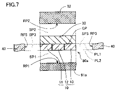
First, composite substrate 80P is arranged on heating element 91a such that
SiC
substrate group 10 faces a first radiation plane RP 1 of first heating element
91 a. Thus,
in a first space SP I (Fig. 7) extending from SiC substrate group 10 in a
direction
perpendicular to first plane PLI and away from support portion 30, first
radiation plane
RP1 faces SiC substrate group 10.
Secondly, a second radiation plane RP2 of second heating element 92 is
arranged
on composite substrate 80P so as to face support portion 30. Each of first and
second
heating elements 91 a and 92 is arranged outside a third space SP3 (Fig. 7)
extending
from gap GP along first plane PL I. Thus, in a second space SP2 (Fig. 7)
extending
from support portion 30 in a direction perpendicular to first plane PL1 and
away from
SiC substrate group 10, second radiation plane RP2 faces support portion 30.
Thirdly, heater 50 is arranged outside third space SP3 (Fig. 7) extending from
gap GP along first plane PLI. More specifically, heater 50 is arranged in a
space
including support portion 30 (a space above first plane PLI in Fig. 5), of the
spaces
separated from each other by the third space. Thus, in third space SP3 (Fig.
7), a
radiation plane RP3 of heat-insulating vessel 40 faces SiC substrate group 10.
Then, support portion 30 and SiC substrates 11 and 12 are heated by heater 50.
This heating step will be described below.
Initially, an atmosphere in heat-insulating vessel 40 is set to an atmosphere
obtained by reducing an atmospheric pressure. Preferably, a pressure of the
atmosphere is set to a pressure higher than 10-' Pa and lower than 104 Pa.
-10-
CA 02758266 2011-10-07
110272-WO-00 : 910426
It is noted that the atmosphere above may be an inert gas atmosphere. As an
inert gas, for example, a noble gas such as He or Ar, a nitrogen gas, or a gas
mixture of
a noble gas and a nitrogen gas can be used. In using this gas mixture, a ratio
of the
nitrogen gas is set, for example, to 60 %. In addition, a pressure in a
treatment
chamber is set preferably to 50 kPa or lower and more preferably to 10 kPa or
lower.
Then, respective temperatures of first radiation plane RP I of first heating
element 91 a, second radiation plane RP2 of second heating element RP2, and
third
radiation plane RP3 of heat-insulating vessel 40 are set to first to third
temperatures.
The second temperature is set higher than the first temperature. In addition,
the third
temperature is set lower than the second temperature and preferably lower than
the first
temperature.
Referring to Fig. 8, as the second temperature is set higher than the first
temperature, a temperature on a second side ICb which is a side of SiC
substrate group
10 facing support portion 30 is higher than a temperature on a first side ICt
which is a
side of SiC substrate group 10 facing first heating element 91 a. Namely, a
temperature
gradient is produced in a direction of thickness of SiC substrate group 10 (a
vertical
direction in Fig. 8). This temperature gradient causes generation of a
sublimate and
travel thereof as shown with an arrow in the drawing, from a region within gap
GP at a
relatively high temperature closer to second side ICb to a region at a
relatively low
temperature closer to first side ICt, of the surfaces of SiC substrates 1 I
and 12, that is,
first and second side surfaces S I and S2.
Referring further to Fig. 9, the sublimate above forms bonded portion BDa
closing opening CR in such a manner as connecting side surfaces Si and S2 to
each
other. Consequently, gap GP (Fig. 8) becomes a gap VDa (Fig. 9) closed by
bonded
portion BDa.
It is noted that experiments for verifying heating temperatures above were
conducted. Then, there were such problems that bonded portion BDa was not
sufficiently formed when a temperature of heater 50 was set to 1600 C and that
SiC
-11-
CA 02758266 2011-10-07
110272-WO-00 : 910426
substrates 11 and 12 were damaged when it was set to 3000 C. These problems,
however, were not seen at each temperature of 1800 C, 2000 C, and 2500 C.
In addition, a pressure of an atmosphere during heating above was verified,
with
a set temperature of heater 50 being fixed at 2000 C. Consequently, there was
a
problem that no bonded portion BDa was formed at 100 kPa and bonded portion
BDa
was less likely to be formed at SO kPa, however, this problem was not seen at
each
pressure of 10 kPa, 100 Pa, 1 Pa, 0.1 Pa, and 0.0001 Pa.
Then, a case where a part of heater 50 is assumed to be located in a .space
between first and second planes PLl and PL2 will be described as a comparative
example (Fig. 10). In this case, at least a part of third radiation plane RP3
(Fig. 7) is
implemented not by heat-insulating vessel 40 but by heater 50. Consequently, a
temperature of at least a part of third radiation plane RP3 becomes higher
than a
temperature of second radiation plane RP2, and hence strong heat radiation
from third
radiation plane RP3 to gap GP occurs. Influence by this strong heat radiation
disturbs
the temperature gradient between first and second sides ICt and ICb in gap GP.
Consequently, since travel of the sublimate (the arrow in Figs. 8 and 9) is
disturbed,
bonded portion BDa is not formed or formation of bonded portion BDa takes
time.
Namely, in the comparative example, opening CR is less likely to be closed.
In contrast, according to the present embodiment, since the temperature of
third
radiation plane RP3 (Fig. 7) (third temperature) is lower than the temperature
of second
radiation plane RP2 (second temperature), influence by heat radiation from
third
radiation plane RP3 to gap GP is weaker than that by heat radiation from
second
radiation plane RP2. Therefore, disturbance of the temperature gradient along
gap GP
produced by temperature difference between first and second radiation planes
RP 1 and
RP2, due to heat radiation from third radiation plane RP3, is lessened.
Consequently,
since the temperature gradient above is more reliably produced, bonded portion
BDa
formed by the sublimate closing opening CR of the gap can more reliably be
formed.
Namely, the opening of gap VDa of semiconductor substrate 80a (Figs. I and 2)
-12-
CA 02758266 2011-10-07
110272-WO-00 : 910426
obtained with the present manufacturing method is more reliably closed by
bonded
portion BDa. Therefore, in the process for manufacturing a semiconductor
device
including semiconductor substrate 80a, introduction of foreign matters in gap
VDa is
less likely and hence lowering in yield attributed to foreign matters is
suppressed.
In addition, semiconductor substrate 80a (Fig. 2) includes both of first and
second front surfaces F 1 and F2 of the respective SiC substrates, as a
substrate surface
on which a semiconductor device such as a transistor is to be formed. Namely,
semiconductor substrate 80a has a substrate surface greater than in a case
where any of
SiC substrates 11 and 12 is used alone. Thus, a semiconductor device can
efficiently
be manufactured with the use of semiconductor substrate 80a.
Though SiC substrate group 10 is arranged on first heating element 91 a in the
present embodiment, a flexible member such as a graphite sheet may be arranged
between SiC substrate group 10 and first heating element 91 a. As this member
closes
opening CR (Fig. 8), travel of the sublimate (the arrow in Fig. 8) is more
reliably
blocked in opening CR and hence bonded portion BDa is more likely to be formed
in
opening CR.
In addition, before bonded portion BDa is formed, a protection film such as a
resist film may be formed in advance on first and second front surfaces Fl and
F2.
Thus, sublimation and resolidification on first and second front surfaces Fl
and F2 can
be avoided. Therefore, roughening of first and second front surfaces F 1 and
F2 can be
prevented.
(Embodiment 2)
In the present embodiment, a method of manufacturing composite substrate 80P
(Figs. 3 and 4) employed in Embodiment 1 will be described in detail, in
particular with
reference to a case where support portion 30 is composed of silicon carbide.
For the
sake of brevity of illustration below, only SiC substrates 11 and 12 among SiC
substrates 11 to 19 (Figs. 3 and 4) may be mentioned, however, SiC substrates
13 to 19
are also addressed similarly to SiC substrates 11 and 12.
-13-
CA 02758266 2011-10-07
110272-WO-00:910426
Referring to Fig. 11, SiC substrates I 1 and 12 each having a single-crystal
structure are prepared. Specifically, for example, SiC substrates 11 and 12
are
prepared by cutting an SiC ingot grown on the (0001) plane in hexagonal system
along a
(03-38) plane. Preferably, roughness Ra of back surfaces B 1 and B2 is not
greater
than 100 m.
Then, SiC substrates 11 and 12 are arranged on a first heating element 81 in a
treatment chamber such that each of back surfaces B 1 and B2 is exposed in one
direction (upward in Fig. 11). Namely, SiC substrates 11 and 12 are arranged
side by
side when viewed two-dimensionally.
Preferably, arrangement above is done such that back surfaces B 1 and B2 are
flush with each other or first and second front surfaces F 1 and F2 are flush
with each
other.
In addition, preferably, a shortest distance between SiC substrates 11 and 12
(a
shortest distance in a lateral direction in Fig. 11) is set to 5 mm or
shorter, more
preferably to 1 mm or shorter, further preferably to 100 m or shorter, and
still further
preferably to 10 m or shorter. Specifically, for example, substrates
identical in
rectangular shape are arranged in matrix at a distance not greater than 1 mm
from one
another.
Then, support portion 30 (Fig. 4) connecting back surfaces B 1 and B2 to each
other is formed as follows.
Initially, each of back surfaces B I and B2 exposed in one direction (upward
in
Fig. 11) and a surface SS of a solid source material 20 arranged in one
direction (above
in Fig. 11) with respect to back surfaces B I and B2 are opposed to each other
at a
distance D1 from each other. Preferably, an average value of distance DI is
not
smaller than 1 m and not greater than 1 cm.
Solid source material 20 is made of SIC and it is preferably a solid of a lump
of
silicon carbide specifically implemented, for example, as an SiC wafer. A
crystal
structure of SiC representing solid source material 20 is not particularly
limited. In
-14-
CA 02758266 2011-10-07 110272-WO-00 : 910426
addition, preferably, surface SS of solid source material 20 has roughness Ra
not greater
than 1 mm.
In order to more reliably provide distance D1 (Fig. 11), a spacer 83 (Fig. 14)
having a height corresponding to distance D 1 may be employed. This method is
particularly effective when the average value of distance D1 is not smaller
than about
100 pm.
Then, first heating element 81 heats SiC substrates 11 and 12 to a prescribed
substrate temperature. In addition, a second heating element 82 heats solid
source
material 20 to a prescribed source material temperature. As solid source
material 20 is
heated to the source material temperature, SiC sublimes at surface SS of the
solid
source material so that a sublimate, that is, a gas, is generated. This gas is
supplied
from one direction (above in Fig. 11) onto each of back surfaces B 1 and B2.
Preferably, the substrate temperature is set lower than the source material
temperature, and more preferably temperature difference therebetween is not
smaller
than 1 C and not greater than 100 C. In addition, preferably, the substrate
temperature is not lower than 1800 C and not higher than 2500 C.
Referring to Fig. 12, the gas supplied as above is solidified and
recrystallized on
each of back surfaces B 1 and B2. Thus, a support portion 30p connecting back
surfaces B I and B2 to each other is formed. In addition, as solid source
material 20
(Fig. 11) is consumed and made smaller to thereby become a solid source
material 20p.
Referring mainly to Fig. 13, as sublimation further proceeds, solid source
material 20p (Fig. 12) vanishes. Thus, support portion 30 connecting back
surfaces B 1
and B2 to each other is formed.
Preferably, when support portion 30 is formed, an atmosphere in the treatment
chamber is an inert gas. As an inert gas, for example, a noble gas such as He
or Ar, a
nitrogen gas, or a gas mixture of a noble gas and a nitrogen gas can be used.
In using
this gas mixture, a ratio of the nitrogen gas is set, for example, to 60 %. In
addition, a
pressure in the treatment chamber is set preferably to 50 kPa or lower and
more
- 15 -
CA 02758266 2011-10-07 110272-WO-00 :910426
preferably to 10 kPa or lower.
In addition, preferably, support portion 30 has a single-crystal structure.
More
preferably, inclination of a crystal plane of support portion 30 on back
surface B 1 with
respect to a crystal plane of back surface B I is not greater than 10 , and
inclination of a
crystal plane of support portion 30 on back surface B2 with respect to a
crystal plane of
back surface B2 is not greater than 10 . These relations of angle are readily
realized,
as support portion 30 is epitaxially grown on each of back surfaces B 1 and
B2.
It is noted that SiC substrate 11, 12 preferably has a hexagonal crystal
structure
and more preferably the crystal structure is 4H-SiC or 6H-SiC. In addition,
SiC
substrates 11 and 12 and support portion 30 are preferably formed of SiC
single crystals
identical in crystal structure.
Moreover, preferably, concentration in each of SiC substrates 11 and 12 is
different from impurity concentration in support portion 30. More preferably,
the
impurity concentration in support portion 30 is higher than impurity
concentration in
each of SiC substrates 11 and 12. It is noted that SiC substrate 11, 12 has
impurity
concentration, for example, not lower than 5 x 10¹⁶ CM -3 and not higher than
5 x 10¹⁹
cm 3. Meanwhile, support portion 30 has impurity concentration, for example,
not
lower than 5 x 10¹⁶ CM -3 and not higher than 5 x 10²¹ CM-3 . For example,
nitrogen or
phosphorus can be employed as the impurity above.
In addition, preferably, an off angle of first front surface F 1 with respect
to the
{0001 } plane of SiC substrate 11 is not smaller than 50 and not greater than
65 , and
an off angle of second front surface F2 with respect to the { 0001 } plane of
the SiC
substrate is not smaller than 50 and not greater than 65 .
More preferably, an angle between an off orientation of first front surface F
1 and
a <1-100> direction of SiC substrate 11 is not greater than 5 and an angle
between an
off orientation of second front surface F2 and a <1-100> direction of
substrate 12 is not
greater than 5 .
Further preferably, an off angle of first front surface F1 with respect to the
{03-
-16-
CA 02758266 2011-10-07 110272-WO-00:910426
38} plane in the <1-100> direction of SiC substrate I 1 is not smaller than -3
and not
greater than 5 , and an off angle of second front surface F2 with respect to
the { 03-38)
plane in the <1-100> direction of SiC substrate 12 is not smaller than -3 and
not
greater than 5 .
In the above, the "off angle of first front surface Fl with respect to the (03-
38)
plane in the <1-100> direction" refers to an angle formed between a normal of
the (03-
381 plane and an orthogonal projection of a normal of first front surface F 1
onto a
projection surface where the <1-100> direction and the <0001> direction
extend, and
the sign is positive when the orthogonal projection above is closer to
parallel to the <1-
100> direction, and the sign is negative when the orthogonal projection above
is closer
to parallel to the <0001> direction. This is also the case with the "off angle
of second
front surface F2 with respect to the {03-38} plane in the <1-100> direction."
In addition, preferably, an angle between the off orientation of first front
surface
F1 and a <11-20> direction of substrate 11 is not greater than 5 , and an
angle between
the off orientation of second front surface F2 and a <11-20> direction of
substrate 12 is
not greater than 5 .
According to the present embodiment, since support portion 30 formed on each
of back surfaces B I and B2 is made of SiC similarly to SiC substrates 11 and
12, various
physical properties are close between the SiC substrate and support portion
30.
Therefore, warp or crack of composite substrate 80P (Figs. 3 and 4) or
semiconductor
substrate 80a (Figs. 1 and 2) due to difference in these various physical
properties can
be suppressed.
In addition, by employing a sublimation method, high-quality support portion
30
can quickly be formed. Further, if a close-space sublimation method, is
particularly
employed as the sublimation method, support portion 30 can more uniformly be
formed.
Moreover, as the average value of distance D I (Fig. 11) between each of back
surfaces B I and B2 and the surface of solid source material 20 is not greater
than 1 cm,
film thickness distribution of support portion 30 can be less. Further, as the
average
-17-
CA 02758266 2011-10-07 1 10272-WO-00 : 910426
value of this distance DI is not smaller than I m, a space where SIC sublimes
can
sufficiently be secured.
Furthermore, in the step of forming support portion 30, a temperature of SiC
substrates 1 I and 12 is set lower than a temperature of solid source material
20 (Fig. 11).
Thus, SiC that sublimes can efficiently be solidified on SiC substrates I 1
and 12.
In addition, preferably, the step of arranging SiC substrates 11 and 12 is
performed such that a shortest distance between SiC substrates 11 and 12 is
not greater
than 1 mm. Thus, support portion 30 can be formed such that back surface B 1
of SiC
substrate 11 and back surface B2 of SiC substrate 12 are more reliably
connected to
each other.
Moreover, preferably, support portion 30 has a single-crystal structure.
Various physical properties of support portion 30 are thus close to those of
each of SiC
substrates II and 12 similarly having a single-crystal structure.
Further preferably, inclination of the crystal plane of support portion 30 on
back
surface B I with respect to the crystal plane of back surface B l is not
greater than 10 ,
and inclination of the crystal plane of support portion 30 on back surface B2
with
respect to the crystal plane of back surface B2 is not greater than 10 .
Anisotropy of
support portion 30 can thus be close to anisotropy of each of SiC substrates
11 and 12.
In addition, preferably, each of SiC substrates 11 and 12 is different in
impurity
concentration from support portion 30. Thus, semiconductor substrate 80a (Fig.
2)
having a two-layered structure different in impurity concentration can be
obtained.
In addition, preferably, support portion 30 is higher in impurity
concentration
than each of SiC substrates 1 I and 12. Therefore, support portion 30 can be
lower in
resistivity than each of SIC substrates 11 and 12. Thus, semiconductor
substrate 80a
suitable for manufacturing a semiconductor device in which a current flows in
a
direction of thickness of support portion 30, that is, a vertical
semiconductor device, can
be obtained.
In addition, preferably, an off angle of first front surface FI with respect
to the
- 18 -
CA 02758266 2011-10-07
110272-WO-00 : 910426
{0001 } plane of SiC substrate 11 is not smaller than 50 and not greater than
65 , and
an off angle of second front surface F2 with respect to the { 0001 } plane of
SiC
substrate 12 is not smaller than 50 and not greater than 65 . Thus, channel
mobility at
first and second front surfaces F 1 and F2 can be improved as compared with a
case
where first and second front surfaces F 1 and F2 are { 0001 } planes.
More preferably, an angle between the off orientation of first front surface
FI
and the <1-100> direction of SiC substrate 11 is not greater than 5 and an
angle
between the off orientation of second front surface F2 and the <1-100>
direction of SiC
substrate 12 is not greater than 5 . Thus, channel mobility at first and
second front
surfaces F1 and F2 can further be improved.
Further preferably, an off angle of first front surface F1 with respect to the
{03-
38) plane in the <1-100> direction of SiC substrate 11 is not smaller than -3
and not
greater than 5 , and an off angle of second front surface F2 with respect to
the {03-38}
plane in the <1-100> direction of SiC substrate 12 is not smaller than -3 and
not
greater than 5 . Thus, channel mobility at first and second front surfaces F I
and F2
can still further be improved.
In addition, preferably, an angle between the off orientation of first front
surface
FI and the <11-20> direction of SiC substrate 11 is not greater than 5 , and
an angle
between the off orientation of second front surface F2 and the <11-20>
direction of SiC
substrate 12 is not greater than 5 . Thus, channel mobility at first and
second front
surfaces F I and F2 can be improved as compared with a case where first and
second
front surfaces F1 and F2 are {0001) planes.
Though an SiC wafer has been exemplified as solid source material 20 in the
above, solid source material 20 is not limited thereto, and for example, SiC
powders or
an SiC sintered object may be employed.
In addition, any element capable of heating an object may be employed as first
and second heating elements 81 and 82, and for example, such an element of a
resistance
heating type as using a graphite heater or an element of an induction heating
type can be
-19-
CA 02758266 2011-10-07
110272-WO-00 : 910426
employed.
In addition, in Fig. 11, each of back surfaces BI and B2 is spaced apart from
surface SS of solid source material 20 in its entirety. Each of back surfaces
B i and B2
may be spaced apart from surface SS of solid source material 20, while back
surfaces B 1
and B2 and surface SS of solid source material 20 are partially in contact
with each
other. Two variations corresponding to this case will be described below.
Referring to Fig. 15, in this example, warp of an SiC wafer representing solid
source material 20 ensures the distance above. More specifically, in the
present
example, a distance D2 is locally zero, however, the average value
unexceptionally
exceeds zero. In addition, preferably, the average value of distance D2 is not
smaller
than 1 p.m and not greater than 1 cm, similarly to the average value of
distance D 1.
Referring to Fig. 16, in this example, warp of SiC substrates 11 to 13 ensures
the
distance above. More specifically, in the present example, a distance D3 is
locally zero,
however, the average value unexceptionally exceeds zero. In addition,
preferably, the
average value of distance D3 is not smaller than I m and not greater than 1
cm,
similarly to the average value of distance Dl.
It is noted that combination of the methods in Figs. 15 and 16, that is, both
of
warp of the SiC wafer representing solid source material 20 and warp of SiC
substrates
11 to 13, may ensure the distance above.
The method in each of Figs. 15 and 16 or the method based on combination of
both methods described above is particularly effective when the average value
of the
distance above is not greater than 100 m.
In addition, in order to ensure the distance above, the back surface of each
of
SiC substrates 11 to 13 (for example, back surfaces B I and B2) may be a
surface
formed by slicing. Namely, the back surface may be a surface formed by slicing
but not
polished subsequently. Thus, irregularities are provided on each back surface.
Therefore, a space within a recess in these irregularities can be used for
ensuring the
distance above.
-20-
CA 02758266 2011-10-07
110272-WO-00:910426
(Embodiment 3)
In Embodiment 1, prior to formation of bonded portion BDa (Fig. 2), each of
first and second back surfaces B I and B2 is bonded in advance to support
portion 30,
for example, with the method according to Embodiment 2.
In contrast, in the present embodiment, bonding of each of first and second
back
surfaces BI and B2 to support portion 30 is performed simultaneously with
formation of
bonded portion BDa. Namely, in the present embodiment, the step of bonding
each of
first and second back surfaces B I and B2 of SiC substrate group 10 to support
portion
30 is further included after the step of preparing support portion 30 and SiC
substrate
group 10, and this bonding step is performed simultaneously with the step of
forming
bonded portion BDa (Fig. 2).
It is noted that the present embodiment is otherwise substantially the same as
Embodiment 1 and hence detailed description will not be provided.
According to the present embodiment, the step of bonding each of first and
second back surfaces B 1 and B2 to support portion 30 is performed
simultaneously with
the step of forming bonded portion BDa. Therefore, as compared with a case
where
these steps are individually performed, the process for manufacturing
semiconductor
substrate 80a (Figs. 1 and 2) can be simplified.
In a variation of the present embodiment, solid source material 20 (Fig. 11)
instead of support portion 30 (Fig. 5) may be prepared as the support portion
prepared
before heating, solid source material 20 and SiC substrate group 10 may be
arranged as
in Embodiment 2, and heater 50 may be arranged as in Embodiment 1. In
addition,
here, as in each variation of Embodiment 2, the construction in Fig. 15, the
construction
in Fig. 16, or a construction based on combination thereof may be employed.
(Embodiment 4)
Referring to Figs. 17 and 18, a semiconductor substrate 80b according to the
present embodiment has a gap VDb closed by a bonded portion BDb instead of gap
VDa (Fig. 2: Embodiments I to 3) closed by bonded portion BDa.
-21-
CA 02758266 2011-10-07 110272-WO-00 : 910426
A method of manufacturing semiconductor substrate 80b will now be described.
In the present embodiment, support portion 30 is made of SiC, and even after
bonded portion BDa is formed as shown in Fig. 9, mass transfer involved with
sublimation further continues. Consequently, sublimation from support portion
30 into
closed gap VDa also occurs to an unignorable extent. Namely, a sublimate from
support portion 30 is deposited on bonded portion BDa. Thus, gap VDa between
SiC
substrates 11 and 12 moves in such a manner as partially entering support
portion 30,
and hence gap VDb (Fig. 18) closed by bonded portion BDb is formed.
With semiconductor substrate 80b (Fig. 18) according to the present
embodiment, bonded portion BDb greater in thickness than bonded portion BDa of
semiconductor substrate 80a (Fig. 2) can be formed.
(Embodiment 5)
Referring to Figs. 19 and 20, a semiconductor substrate 80c according to the
present embodiment has a gap VDc closed by a bonded portion BDc instead of gap
VDb (Fig. 18: Embodiment 4) closed by bonded portion BDb. Semiconductor
substrate 80c is obtained by moving entire gap VDa (Fig. 2) into support
portion 30 via
a position of gap VDb (Fig. 18), with the method as in Embodiment 4.
According to the present embodiment, bonded portion BDc further greater in
thickness than bonded portion BDb in Embodiment 4 can be formed.
It is noted that gap VDc may be moved to reach the back surface side (a lower
side in Fig. 20). Thus, closed gap VDc becomes a recess on the back surface
side.
This recess may be removed by polishing.
(Embodiment 6)
Referring mainly to Fig. 21, in the present embodiment, a heat insulator 93 is
arranged to face SiC substrate group 10 in the third space (Fig. 7). Namely,
instead of
heat-insulating vessel 40, heat insulator 93 implements third radiation plane
RP3. Heat
insulator 93 is lower in thermal conductivity than a material forming second
heating
element 92, that is, second radiation plane RP2, and preferably lower in
thermal
-22-
CA 02758266 2011-10-07 110272-WO-00 :910426
conductivity than a material forming a first heating element 91b formed of a
material the
same as that for first heating element 91a (Fig. 5), that is, first radiation
plane RP1.
Such heat insulator 93 is formed, for example, of carbon felt.
According to the present embodiment, a temperature of third radiation plane
RP3 can more reliably be lowered by means of heat insulator 93.
In addition, when a heat-insulating function of heat insulator 93 is
sufficiently
high, the temperature of third radiation plane RP3 formed by heat insulator 93
can be
made lower than the temperature of second radiation plane RP2 even if heater
50 is
located as shown in Fig. 21 with respect to SiC substrate group 10, that is,
even if a part
of heater 50 is located in third space SP3 (Fig. 7). Therefore, according to
the present
embodiment, a degree of freedom in arrangement of heater 50 is higher than in
Embodiment 1.
(Embodiment 7)
Referring to Fig. 22, a heating apparatus in the present embodiment is an
induction heating furnace, and it has a heated element 59 (heat source) and a
coil 159
instead of heater 50 (Fig. 5). Heated element 59 is, for example, a graphite
crucible,
and a substantially closed space is formed in heat-insulating vessel 40. In
this closed
space, first heating element 91 a, second heating element 92, SiC substrate
group 10, and
support portion 30 are arranged. In addition, heat insulator 93 is arranged as
in
Embodiment 6.
In the heating step in the present embodiment, initially, heated element 59
generates heat as a result of induction heating by coil 159. As a result of
this heat
generation, first heating element 91 a and second heating element 92 are
heated.
According to the present embodiment, in a case where an induction heating
furnace is employed, the effect as in Embodiment 6 is obtained. If heat
insulator 93 is
not employed, the construction is as shown in Fig. 23, that is, third
radiation plane RP3
(Fig. 7) being implemented by heated element 59. Therefore, as in the case of
the
construction in Fig. 10 (the comparative example of Embodiment 1), opening CR
(Fig.
- 23 -
CA 02758266 2011-10-07
110272-WO-00 : 910426
8) is less likely to be closed.
(Embodiment 8)
Referring to Fig. 24, in the present embodiment, unlike Embodiment 7, heated
element 59 is not provided but first and second heating elements 91a and 92
are directly
heated through induction heating.
According to the present embodiment, since heat radiation is achieved by the
construction shown in Fig. 7 as in Embodiment 1, the effect as in Embodiment 1
is
obtained.
(Embodiment 9)
Referring to Fig. 25, a heating apparatus in the present embodiment has first
to
third heaters 51 to 53 (first to third heat generation elements) and first to
third heater
power supplies 151 to 153 for heating.
First to third heaters 51 to 53 are arranged in first to third spaces SPI to
SP3
(Fig. 7), respectively. It is noted that third heater 53 does not have to be
arranged in
third space SP3 in its entirety and at least a part thereof should only be
arranged therein.
First to third heater power supplies 151 to 153 are connected so as to be able
to
independently control heat generation by first to third heaters 51 to 53.
Thus,
respective temperatures of the surfaces corresponding to first to third
radiation planes
RP1 to RP3 (Fig. 7) in the present embodiment, that is, the surface of first
heating
element 91a, the surface of second heating element 92, and the surface of
third heater 53,
can be controlled independently of one another. Therefore, the temperature
corresponding to third radiation plane RP3 can be set lower than the
temperature
corresponding to second radiation plane RP2 but not excessively lower than
that.
If temperature control as precise as above is not required, any or both of
first
heater 51 and third heater 53 may be eliminated.
(Appendix 1)
The semiconductor substrate according to the present invention is fabricated
with the following manufacturing method.
-24-
CA 02758266 2011-10-07
110272-WO-00 : 910426
A plurality of silicon carbide substrates having first and second silicon
carbide
substrates and a support portion are prepared. The first silicon carbide
substrate has a
first back surface facing the support portion and located on one plane, a
first front
surface opposed to the first back surface, and a first side surface connecting
the first
back surface and the first front surface to each other. The second silicon
carbide
substrate has a second back surface facing the support portion and located on
one plane,
a second front surface opposed to the second back surface, and a second side
surface
connecting the second back surface and the second front surface to each other.
The
second side surface is arranged such that a gap having an opening between the
first and
second front surfaces is formed between the second side surface and the first
side
surface. The support portion and the first and second silicon carbide
substrates are
heated such that a sublimate is generated from the first and second side
surfaces and a
bonded portion closing the opening is formed thereby. The heating step has the
following steps. A temperature of a first radiation plane facing the plurality
of silicon
carbide substrates in a first space extending from the plurality of silicon
carbide
substrates in a direction perpendicular to one plane and away from the support
portion is
set to a first temperature. A temperature of a second radiation plane facing
the support
portion in a second space extending from the support portion in a direction
perpendicular to one plane and away from the plurality of silicon carbide
substrates is set
to a second temperature higher than the first temperature. A temperature of a
third
radiation plane facing the plurality of silicon carbide substrates in a third
space extending
from the gap along one plane is set to a third temperature lower than the
second
temperature.
It should be understood that the embodiments disclosed herein are illustrative
and non-restrictive in every respect. The scope of the present invention is
defined by
the terms of the claims, rather than the description above, and is intended to
include any
modifications within the scope and meaning equivalent to the terms of the
claims.
INDUSTRIAL APPLICABILITY
- 25 -
CA 02758266 2011-10-07 110272-WO-00:910426
The method of manufacturing a semiconductor substrate according to the
present invention is particularly advantageously applicable to a method of
manufacturing
a semiconductor substrate including a silicon carbide substrate.
DESCRIPTION OF THE REFERENCE SIGNS
10 SiC substrate group (a plurality of silicon carbide substrates); I0a
supported
layer; 1 I SiC substrate (first silicon carbide substrate); 12 SiC substrate
(second silicon
carbide substrate); 13 to 19 SiC substrate; 20, 20p solid source material; 30,
30p
support portion; 40 heat-insulating vessel; 59 heated element; 80a to 80c
semiconductor
substrate; 80P composite substrate; 81, 91 a, 91 b first heating element; 82,
92 second
heating element; 93 heat insulator; 150 heater power supply; 151 to 153 first
to third
heater power supply; and 159 coil.
-26-