Note : Les descriptions sont présentées dans la langue officielle dans laquelle elles ont été soumises.
CA 02758900 2011-11-17
LIGHT EMITTING DIODE RETROFIT SYSTEM FOR
FLUORESCENT LIGHTING SYSTEMS
Inventors: Biju Antony and Shashank Bakre
TECHNICAL FIELD
[0001] The present application relates to solid state lighting sources, and in
particular to a light
emitting diode (LED) retrofit system for fluorescent lighting systems.
BACKGROUND
[0002] Fluorescent lighting is widely used in many applications. One type of
fluorescent
lighting system includes a fluorescent lamp fixture having a ballast coupled
to an alternating
current (AC) voltage source and a plurality of pins for electrically coupling
one or more
fluorescent lamps to the ballast. The ballast may be configured to provide a
regulated AC power
supply to the fluorescent lamps. While fluorescent lighting may be generally
more efficient than
incandescent lighting, fluorescent lighting does suffer from several
drawbacks. One drawback is
that many fluorescent lamps utilize hazardous or toxic materials, such as
phosphorous, mercury,
etc., which may create environmental issues. Another drawback is that the
lifespan of
fluorescent lamps may be significantly shortened in applications in which the
lamp is frequently
switched on and off.
SUMMARY
[0003] Generally, the present disclosure provides systems and methods for
retrofitting one or
more light emitting diode (LED) light sources to a fluorescent lighting
fixture. In particular, a
LED retrofit system including an LED light source may be electrically coupled
to the existing
pins of a fluorescent lighting fixture. The LED retrofit system may receive a
high voltage AC
input from a ballast associated with the fluorescent lighting fixture. The LED
retrofit system
may include transformer circuitry to provide isolation and to step down the
high voltage AC to a
lower AC voltage suitable for driving an LED light source of the LED retrofit
system. A
rectifier may then convert the lower voltage AC to a lower direct current (DC)
voltage. The
Page 1 of 23
CA 02758900 2011-11-17
output of the rectifier, which may have an amount of AC rippling, may
optionally be smoothed,
e.g. through the use of a smoothing capacitor or the like.
[0004] Advantageously, the systems and methods of the present disclosure may
allow a
fluorescent lighting fixture to be retrofitted to power an LED light source
without requiring any
modification of the fluorescent lighting fixture. Additionally, the systems
and methods of the
present disclosure may provide high efficiency that is close to the ballast
efficiency. In addition,
the systems and methods of the present disclosure may offer reduced component
count and/or
size which may translate to increased power factor efficiency, and significant
cost savings over
conventional LED driving systems, and/or may make the LED retrofit system
suitable for a
wider range of applications. Moreover, the systems and methods of the present
disclosure may
include transformer circuitry to provide isolation of the ballast output,
which may reduce and/or
eliminate any potential electrical shocks or hazards during installation and
which may allow for a
broader choice of optical components in the design.
[0005] In an embodiment, there is provided a light emitting diode (LED)
retrofit system for use
with a fluorescent lamp fixture having an existing ballast. The LED retrofit
system includes at
least one LED light source; transformer circuitry configured to receive a high
voltage AC signal
from the existing ballast and to output a low voltage AC signal; rectifier
circuitry configured to
receive the low voltage AC signal and generate a DC voltage to drive the LED
light source; and
at least one pin configured to electrically couple the transformer circuitry
to the existing ballast;
the LED retrofit system being configured to be removably coupled to the
fluorescent lamp
fixture.
[0006] In a related embodiment, the LED retrofit system may further include a
support substrate
having coupled thereto the at least one pin, the LED light source, the
transformer circuitry, and
the rectifier circuitry, wherein the at least one pin may be configured to
removably couple the
LED retrofit system to at least one connector of the fluorescent lamp fixture.
In another related
embodiment, the the rectifier circuitry may include full wave bridge rectifier
circuitry configured
to generate a full wave rectified AC voltage from the low voltage AC signal
from the transformer
circuitry and a filtering capacitor in parallel with the LED light source;
wherein the filtering
capacitor may be configured to filter the full wave rectified AC voltage into
the DC voltage to
drive the LED light source. In yet another related embodiment, the transformer
circuitry mya
include a transformer configured to provide a load for the existing ballast to
operate at rated
Page 2 of 23
CA 02758900 2011-11-17
specifications of the existing ballast. In a further related embodiment, the
transformer circuitry
may include a transformer configured to provide a load of approximately 350 Q.
In another
further related embodiment, the transformer may include a high frequency
transformer
configured to operate at 20 kHz or greater. In a further related embodiment,
the high frequency
transformer may include a primary winding and a secondary winding, the primary
winding
configured to receive the high voltage AC signal from the existing ballast and
the secondary
winding configured to provide the low voltage AC signal having a voltage based
on the LED
light source. In a further related embodiment, the primary side of the
transformer may be tuned
based on the inductance and operating frequency of a fluorescent lamp for
which the existing
ballast was rated.
[00071 In another related embodiment, the LED retrofit system may further
include control
circuitry configured to regulate power to the LED light source. In a further
related embodiment,
the control circuitry may include a controller, switch circuitry, and a
temperature sensor, wherein
the controller may be configured to receive a signal from the temperature
sensor representative
of a temperature of the LED light source and output a PWM signal to control a
conduction state
of the switch circuitry. In another further related embodiment, the control
circuitry may include
a controller, switch circuitry, and current sense circuitry, wherein the
controller may be
configured to receive a signal from the current sense circuitry representative
of a current through
the LED light source and output a signal to control a conduction state of the
switch circuitry to
prevent an over-current situation.
[00081 In another embodiment, there is provided a retrofit lighting system.
The retrofit lighting
system includes a fluorescent lamp fixture and a light emitting diode (LED)
retrofit system
configured to be removably coupled to the fluorescent lamp fixture. The
fluorescent lamp
fixture includes: a frame, an existing ballast configured to be coupled to an
AC power source and
to provide a high voltage AC signal configured to drive a fluorescent lamp,
and at least one
connector coupled to an output of the existing ballast, the at least one
connector configured to be
coupled to the fluorescent lamp. The LED retrofit system includes at least one
pin configured to
be removably coupled to the at least one connector and to receive the high
voltage AC signal
from the existing ballast; at least one LED light source; transformer
circuitry coupled to the at
least one pin and configured to receive the high voltage AC signal and to
output a low voltage
Page 3 of 23
CA 02758900 2011-11-17
AC signal; and rectifier circuitry configured to receive the low voltage AC
signal and generate a
DC voltage to drive the LED light source.
[0009] In a related embodiment, the rectifier circuitry comprises full wave
bridge rectifier
circuitry configured to generate a full wave rectified AC voltage from the low
voltage AC signal
from the transformer circuitry and a filtering capacitor in parallel with the
LED light source;
wherein the filtering capacitor may be configured to filter the full wave
rectified AC voltage into
the DC voltage to drive the LED light source. In another related embodiment,
the transformer
circuitry may include a transformer configured to provide a load for the
existing ballast to
operate at rated specifications of the existing ballast. In a further related
embodiment, the
transformer comprises a primary winding and a secondary winding, the primary
winding
configured to receive the high voltage AC signal from the existing ballast and
the secondary
winding configured to provide the low voltage AC signal having a voltage based
on the LED
light source, wherein primary side of the transformer may be tuned based on
the inductance and
operating frequency of the fluorescent lamp.
[0010] In another related embodiment, the LED retrofit system may further
include control
circuitry comprising a controller, switch circuitry, and a temperature sensor,
wherein the
controller may be configured to receive a signal from the temperature sensor
representative of a
temperature of the LED light source and output a PWM signal to control a
conduction state of
the switch circuitry. In yet another related embodiment, the LED retrofit
system further
comprises control circuitry comprising a controller, switch circuitry, and a
current sense
circuitry, wherein the controller may be configured to receive a signal from
the current sense
circuitry representative of a current through the LED light source and output
a signal to control a
conduction state of the switch circuitry to prevent an over-current situation.
[0011] In an embodiment, there is provided a method of driving a LED light
source using an
existing ballast of a fluorescent lamp fixture. The method includes: receiving
a high voltage AC
signal from the existing ballast of the fluorescent lamp fixture; converting
the high voltage AC
signal into a low voltage AC signal using transformer circuitry; rectifying
the low voltage AC
signal to generate a rectified DC voltage using rectifier circuitry; and
driving the LED light
source with the DC voltage.
[0012] In a related embodiment, the step of rectifying may include a full wave
bridge rectifier
circuitry configured to generate a full wave rectified AC voltage from the low
voltage AC signal
Page 4 of 23
CA 02758900 2011-11-17
from the transformer circuitry and a filtering capacitor in parallel with the
LED light source;
wherein the filtering capacitor may be configured to filter the full wave
rectified AC voltage into
the DC voltage to drive the LED light source; and wherein the transformer
circuitry includes a
transformer having a primary winding and a secondary winding, the primary
winding configured
to receive the high voltage AC signal from the existing ballast and the
secondary winding
configured to provide the low voltage AC signal having a voltage based on the
LED light source,
wherein the primary side of the transformer may be tuned based on the
inductance and operating
frequency of the fluorescent lamp for which the existing ballast was rated
such that the
transformer provides a load for the existing ballast to operate at rated
specifications of the
existing ballast.
BRIEF DESCRIPTION OF THE DRAWINGS
[0013] The foregoing and other objects, features and advantages disclosed
herein will be
apparent from the following description of particular embodiments disclosed
herein, as
illustrated in the accompanying drawings in which like reference characters
refer to the same
parts throughout the different views. The drawings are not necessarily to
scale, emphasis instead
being placed upon illustrating the principles disclosed herein.
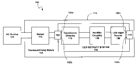
[0014] FIG. 1 is a system diagram illustrating a retrofit lighting system
including a LED retrofit
system according to embodiments described herein.
[0015] FIG. 2 is a system diagram illustrating the LED retrofit system of FIG.
1 in more detail,
according to embodiments described herein.
[0016] FIG. 3 is a circuit diagram illustrating a retrofit lighting system
according to
embodiments described herein.
[0017] FIG. 4 includes plots of current and voltage vs. time, illustrating
performance of the
retrofit lighting system shown in FIG. 3.
[0018] FIG. 5 is a circuit diagram illustrating an LED retrofit system
according to embodiments
described herein.
[0019] FIG. 6 is a block flow diagram illustrating a method according to
embodiments described
herein.
Page 5 of 23
CA 02758900 2011-11-17
DETAILED DESCRIPTION
[0020] The present disclosure is not intended to be limited to the specific
forms set forth herein.
It is understood that various omissions and substitutions of equivalents are
contemplated as
circumstances may suggest or render expedient. It should be understood that
the phraseology
and terminology used herein is for the purpose of description and should not
be regarded as
limiting.
[0021] FIG. 1 is a system diagram illustrating a retrofit lighting system 100
according to
embodiments described herein. In FIG. 1, the retrofit lighting system 100
includes an AC
voltage source 102, a fluorescent lamp fixture 104, and an LED retrofit system
106. The AC
voltage source 102 is configured to generate an AC voltage, e.g., a sinusoidal
AC voltage. For
example, the AC voltage source 102 may include a 120 VAC/60 Hz, 277 VAC/60 Hz,
204
VAC/60 Hz and/or 220V-240 VAC/50 Hz, 347 VAC/60 Hz power source. Those skilled
in the
art will recognize that other types of AC power sources 102 may be used to
drive a retrofit
lighting system 100.
[0022] The fluorescent lamp fixture 104 may include any fluorescent lamp
fixture design and
may include one or more connectors 108, 110 configured to mechanically and/or
electrically
connect with one or more fluorescent lamps (not shown). The connectors 108,
110 may be
coupled to a frame 112 and may take any connector configuration for coupling
with a fluorescent
lamp, such as, but not limited to, a standard linear cylindrical tube T8, T10,
T12 configuration, a
U-shaped curved lamp configuration, a circular T5 lamp configuration, a
compact fluorescent
lamps (CFLs) configuration, a PL lamps configuration, etc.
[0023] The fluorescent lamp fixture 104 may also include one or more ballasts
114. The output
of the ballast 114 may be coupled, either directly or indirectly, to one or
more of the connectors
108, 110. The ballast 114 may be configured to provide proper voltage at the
connectors 108,
110 to establish an arc between the electrodes of the fluorescent lamp (not
shown) and to provide
a controlled amount of electrical energy to the fluorescent lamp, i.e., to
control the amount of
current to the fluorescent lamp using a controlled voltage based on the
designed operating
specifications of the fluorescent lamp. For example, the ballast 114 may be
configured to supply
an output voltage in the range of 200-600 VAC (e.g., 400 VAC), operating at a
frequency of 25
kHz to 100 kHz. The design of the ballast 114 may be determined, at least in
part, based on the
AC voltage source 102 and the number and types of fluorescent lamps. The
ballast 114 may, for
Page 6 of 23
CA 02758900 2011-11-17
example, be configured as a magnetic ballast, an electronic ballast, and/or a
hybrid ballast of a
variety of types, such as but not limited to instant start, rapid start,
and/or programmable ballasts.
The ballast 114 may form an integral component with the frame 112 and/or may
be removably
coupled thereto, e.g., to allow replacement of the ballast 114.
[0024] The LED retrofit system 106 may be coupled to the ballast 114 through
the connectors
108, 110. As shown in FIG. 1, the LED retrofit system 106 includes transformer
circuitry 116,
rectifier circuitry 118, an LED light source 120, and one or more electrical
and/or mechanical
connectors (e.g., pins 122a-n). The LED light source 120 may include one or
more LEDs
coupled to a support substrate 124. In some embodiments, for example, the LED
light source
120 may include one or more arrays of multiple LEDs coupled in series or LED
strips which
may be simultaneously and/or independently controlled. The LEDs in the LED
light source 120
may include any solid state light source and/or semiconductor light source
such as, but not
limited to, conventional high-brightness semiconductor LEDs, organic light
emitting diodes
(OLEDs), bi-color LEDs, tri-color LEDs, polymer light-emitting diodes (PLED),
electro-
luminescent strips (EL), etc. The LEDs in the LED light source 120 may
include, but are not
limited to, packaged and non-packaged LEDs, chip-on-board LEDs, as well as
surface mount
LEDs. The LEDs may also include LEDs with phosphor or the like for converting
energy
emitted from the LED to a different wavelength of light.
[0025] In addition to the LED light source 120, the transformer circuitry 116,
the rectifier
circuitry 118, and the pins 122a-n may all be coupled to the support substrate
124, such that the
entire LED retrofit system 106 may be removably coupled to the connectors 108,
110 of the
fluorescent lamp fixture 104. As further illustrated in FIG. 2, the pins 122a-
n may be fitted with
end caps 121a, 121b disposed at opposite ends of the support substrate 124.
The end caps 121a-
b may be configured to space the pins 122a-n such that the pins 122a-n mate
(electrically and/or
mechanically) with the connectors 108, 110 shown in FIG. 1. The overall size
and/or shape of
the LED retrofit system 106 (for example, the support substrate 124) may be
equivalent to that of
a standard fluorescent tube that the LED retrofit system 106 is intended to
replace.
[0026] The support substrate 124, as shown in FIG. 2, may include one or more
printed circuit
boards (PCBs) and/or other substrates to which the transformer circuitry 116,
the rectifier
circuitry 118, the LED light source 120, and the pins 122a-n may be coupled.
The support
substrate 124 may optionally include one or more optics 126, such as but not
limited to a
Page 7 of 23
CA 02758900 2011-11-17
diffuser, a lens, or the like. The optic 126 may be configured to shape the
light provided by the
LED light source 120 so that a desired viewing angle and/or distribution
pattern is achieved. The
optic 126 may be disposed about only a portion of the support substrate 124
(e.g., in an area
proximate to the LED light source 120), may generally cover the entire support
substrate 124,
and/or may be disposed on each LED or a subset of LEDs within the LED light
source 120.
[00271 Accordingly, while the LED retrofit system 106 may be removably coupled
to the
fluorescent lamp fixture 104, the LED retrofit system 106 is considered a
separate and distinct
component from the fluorescent lamp fixture 104. The LED retrofit system 106
may therefore
be retrofitted into a fluorescent lamp fixture 104 that was designed to be
used with a fluorescent
lamp (not shown). The LED retrofit system 106 may thus function as a direct
replacement light
source for the original equipment fluorescent lamp fixture 104 without the
need to remove the
ballast 114 or to make modifications to the wiring of the existing (e.g.,
installed) fluorescent
lamp fixture 104.
[00281 The transformer circuitry 116 may provide isolation of the high voltage
output of the
ballast 114 from the remainder of LED retrofit system 106. Providing such
isolation may
advantageously allow the transformer circuitry 116 to provide power to a
broader range of
components, e.g., LED light sources 120, while reducing and/or eliminating
hazardous voltages
in the remainder of the LED retrofit system 106 and reducing and/or
eliminating crosstalk
between various channels. In general, the transformer circuitry 116 may step
down the high AC
input voltage generated by the ballast 114 to a lower AC output voltage. The
lower AC output
voltage of the transformer circuitry 116 may depend upon, at least in part,
the number and type
of LEDs used in the LED light source 120. The transformer circuitry 116 may be
coupled to the
ground, thus eliminating a floating condition. Because the ballast 114 may
operate at a high
frequency (such as, but not limited to, at least 20 kHz, e.g., 40 kHz or
more), the transformer
circuitry 116 may include a high frequency transformer 117 configured to be
compatible with the
frequency of the ballast 114, as shown in FIG. 2. For example, the high
frequency transformer
117 may be a known transformer configuration including ferrites that work
efficiently at high
frequency, e.g. 25 kHz to 100 kHz. In general, the transformer 117 may include
a primary
winding and one or more secondary windings (e.g. L2 and L3, respectively, as
shown in FIG. 3)
to achieve isolation of the high voltage output of the ballast 114 from the
remainder of the LED
retrofit system 106. The turn ratio between the primary and secondary windings
may determine
Page 8 of 23
CA 02758900 2011-11-17
the voltage delivered by the transformer circuitry 116. Use of a high
frequency transformer 117
may allow for reduced size of the transformer circuitry 116 and, in turn,
reduced the size of the
overall LED retrofit system 106.
[0029] The rectifier circuitry 118 may include any rectifier to convert the AC
output from the
transformer circuitry 116 into a DC output (or a form of DC output). For
example, the rectifier
circuitry 118 may include a full-wave rectifier. Optionally, the rectifier
circuitry 118 may
include a smoothing circuit or filter 128. The smoothing circuit/filter 128
may reduce the ripple
associated with the full-wave rectifier 118 to produce a substantially stable
DC voltage output
from the AC voltage. For example, the smoothing circuit/filter 128 may include
a reservoir
capacitor or smoothing capacitor placed at the DC output of the rectifier 118.
While the filter
capacitor 128 may smooth the rectified DC voltage into a DC or quasi-DC
signal, such a
smoothed signal may still exhibit significant AC variations in relation to the
peak-to-peak values
of the AC source 102. Thus, to reduce or eliminate visually perceptible
flicker due to the
incomplete smoothing effect of the filter capacitor, filter capacitor 128 may
be selected to have a
time constant, based on, for example, the operating frequency of the AC source
102 and the
required supply current to the LED light source 120. To further reduce this
ripple, a known
capacitor-input filter can be used. This may complement the reservoir
capacitor with a choke
(inductor) and a second filter capacitor, so that a steadier DC output can be
obtained across the
terminals of the filter capacitor 128.
[0030] Turning now to FIG. 3, there is shown a circuit diagram of a retrofit
lighting system
100a. The retrofit lighting system 100a may include ballast circuitry 114a,
transformer circuitry
116a, rectifier circuitry l 18a, and a LED light source 120a. The ballast
circuitry 114a may be an
existing ballast associated with a fluorescent lighting system. As used
herein, the phrase
"existing ballast" is intended to refer to a ballast which was designed and/or
sold for use with a
fluorescent lamp of a fluorescent lighting system, not for a LED-based
lighting system. The
ballast circuitry 114a may include one or more inductors L1 and ballast
capacitors Cl, C2
electrically coupled to an AC signal V 1, for example, a 120 V/60 Hz AC
signal. The ballast
circuitry 114a (e.g., an existing ballast) may be designed to operate at a
specified frequency and
load, such as, but not limited to, 40 kHz and 350 ohms at 600 VAC, based on
the fluorescent
lamp configuration it is intended to drive. The ballast circuitry 114a may be
designed based on
standard, generally accepted operating parameters established for fluorescent
lamps, for
Page 9 of 23
CA 02758900 2011-11-17
example, by the Underwriters Laboratories, Inc. (UL), United States
Occupational Safety and
Health Administration (OSHA), CE mark, industry standards, or the like.
[0031] The output of the ballast circuitry 114a may be coupled to the
transformer circuitry 116a,
e.g. through connectors, such as the connectors 108, 110 shown in FIG. 1. The
transformer
circuitry 116a may include a high frequency transformer 117a including a
primary winding L2
and a secondary winding L3. In particular, the output of the ballast circuitry
114a may be
received by the primary side winding L2, which, in combination with the
secondary winding L3,
may step down the AC voltage from the ballast circuitry 114a to a lower AC
voltage on the
secondary winding L3. The turn ratio between the primary and secondary
windings L2, L3 may
determine the voltage delivered by the transformer circuitry 116a, and may be
based on, at least
in part, the minimum voltage necessary to drive the LED light source 120a.
[0032] The transformer circuitry 116a may be configured to be compatible with
the design
specifications of the ballast circuitry 114a. For example, the transformer
circuitry 11 6a may be
configured to provide a load to the ballast circuitry 114a that approximates
the load the that the
ballast circuitry 114a was designed to drive in order to deliver maximum power
(e.g., but not
limited to, 350 ohms at 40 kHz). The transformer circuitry 116a may also be
configured to
operate at and/or near the operating frequency of the ballast circuitry 114a
(e.g., but not limited
to, 40 kHz). The primary winding L2 of the transformer circuitry 116a may
optionally be
coupled to the ground 332, for example, through a resistor R3.
[0033] The rectifier circuitry 118a may be coupled to the output of the
transformer circuitry 116a
and may be configured to rectify and filter the AC output of the transformer
circuitry 116a. As
shown in FIG. 3, the rectifier circuitry 118a includes four diodes D 1-D4
arranged in a full-wave
bridge to rectify the AC output of the transformer circuitry 116a into a full-
wave-rectified DC
output. This arrangement is known as a full wave rectifier, and may be
referred to herein as
either a full wave bridge, FWB or full wave rectifier. A filter capacitor Cf
may be provided to
filter the rectified DC output of the full wave rectifier and generate a DC or
quasi-DC output
with reduced ripple. While the filter capacitor Cf may smooth the rectified DC
output into a DC
or quasi-DC signal, such a smoothed signal may still exhibit significant AC
variations in relation
to the peak-to-peak values of an AC source providing power to the system, such
as the AC
source 102 shown in FIG. 1. Thus, to reduce or eliminate visually perceptible
flicker due to the
incomplete smoothing effect of the filter capacitor Cf, the filter capacitor
Cf may be selected to
Page 10 of 23
CA 02758900 2011-11-17
have a time constant, based on, for example, the operating frequency of the AC
source and the
required supply voltage for driving the LED light source 120a.
[0034] In FIG. 3, the LED light source 120a includes a plurality of LEDs 321 a-
n connected in
series across the DC output of the rectifier circuitry 118a, i.e. across the
filter capacitor Cf. The
output of the rectifier circuitry 118a may thus drive the LEDs 321a-n, causing
the LEDs 321a-n
to emit light. The LED light source 120a may optionally be coupled to ground
332, which may
include, for example, a system MAINS ground and/or common (earth) ground.
Coupling the
LED light source 120a to the ground 332 may prevent the LED light source 120a
from being in a
"floating" state, which may reduce or eliminate electro-magnetic interference
(i.e., noise)
emanated or received by the LED light source 120a. While a single LED light
source 120a is
shown, the LED light source 120a may include a plurality of LED light sources
120a, each of
which may contain a different number and/or type of LEDs 32la-n. For example,
the
transformer circuitry 11 6a may include a plurality of secondary windings L3
configured to drive
a plurality of LED channels (e.g., a plurality of LED light sources 120a) from
a single AC
voltage source V1, and each LED channel may be provided with its own rectifier
circuit 118a.
[0035] FIG. 4 includes plots 402, 404, 406, 408 of current and voltage vs.
time, illustrating
performance of the retrofit lighting system 100a illustrated in FIG. 3. In
particular, the plot 402
illustrates an exemplary output of the ballast circuitry 114a shown in FIG. 3.
As shown, the
voltage at the output of the ballast circuitry may be approximately 200 VAC
(400 VAC peak-to-
peak). The plot 404 illustrates the output of the transformer circuitry 116a,
i.e., the output of the
secondary winding L3, in response to the ballast circuitry output voltage
illustrated in the plot
402. As shown, the voltage at the output of the transformer circuitry may be
approximately 40
VAC. The plot 406 illustrates the output of the rectifier circuitry 118a,
i.e., the rectified DC
voltage to the LED light source 120a, in response to the transformer circuitry
116a output
voltage illustrated in the plot 404. As shown, the voltage at the output of
the rectifier circuitry
118a may be approximately 40 VDC. The plot 408 illustrates the current drawn
by the LED
light source 120a in response to the rectifier circuitry 11 8a output voltage
illustrated in the plot
406. As shown, the retrofit lighting system 100a may provide a substantially
constant voltage
and/or current to drive the LED light source 120a using existing ballast
circuitry 114a.
[0036] FIG. 5 illustrates a retrofit lighting system 100b. The illustrated
retrofit lighting system
100b includes ballast circuitry 114, transformer circuitry 116, rectifier
circuitry 118, and a LED
Page 11 of 23
CA 02758900 2011-11-17
light source 120, all configured as described above in connection with FIGs. 1-
3. The retrofit
lighting system 100b also includes control circuitry 550. The control
circuitry 550 may be
configured to control the power to the LED light source 120. For example, the
control circuitry
550 may be configured to control the power delivered to the LED light source
120 in the event of
an over-current situation, e.g., to prevent damage to the LED light source
120, and/or to
compensate for temperature changes of the LED light source 120, e.g., to
provide a constant
overall brightness (luminosity) from the LED light source 120. In some
embodiments, the
control circuitry 550 may include a controller 552, a temperature sensor 554,
and switch circuitry
556. The controller 552 may include a processor, microcontroller, application
specific integrated
circuit (ASIC), or the like, configured to receive a signal from the
temperature sensor 554 that is
representative of the temperature of the LED light source 120, e.g., the
temperature of the LEDs
within LED light source 120 and/or the ambient temperature proximate to the
LED light source
120. The controller 552 may then compare this signal to a value stored in a
look-up table (LUT)
558 and generate a pulse-width modulated (PWM) signal 560 based on the
difference to control
the conduction state of the switch circuitry 556. While the switch circuitry
556 is depicted as a
generalized switching circuit, those skilled in the art will recognize that
the switch circuitry 556
may include an FET switch (e.g., but not limited to, a MOSFET), BJT switch or
other circuitry
capable of switching conduction states.
[00371 As is known, the PWM signal 560 generated by the controller 552 may
have a
controllable duty cycle to control the brightness and/or color of the LED
light source 120. For
example, assuming a 50% duty cycle, drive current is delivered to the LED
light source 120
during the ON time of the switch circuitry 556 and interrupted during the OFF
time of the switch
circuitry 556. To control the overall brightness of the light output from the
LED light source
120, the duty cycle of the PWM signal 560 may be adjusted. For example, the
duty cycle may
range from 0% (switch is always open) to 100% (switch is always closed) to
control the overall
brightness (luminosity) and/or color of the LED light source 120. When the PWM
signal 560 is
ON (high), the switch circuitry 556 may close, thus creating a conduction path
through the
switch circuitry 556, the LED light source 120, and the rectifier circuitry
118. When the PWM
signal 560 is OFF, the switch circuitry 556 may open thus decoupling the LED
light source 120
and the switch circuitry 556 from the rectifier circuitry 118. Accordingly,
the current flowing
through the LED light source 120 may be regulated, thereby allowing the
luminosity of the LED
Page 12 of 23
CA 02758900 2011-11-17
light source 120 to be corrected for temperature. The frequency of the PWM
signal 560 may be
selected to prevent visually perceivable flicker from the LED light source
120.
[0038] In addition or alternatively, the control circuitry 550 may include
current sense circuitry
562. According to some embodiments, the current sense circuitry 562 may
produce a signal 564
representative of the current flowing through the LED light source 120, for
example, using a
sense resistor Rsense= The controller 552 may receive the signal 564 and
compare this to one or
more threshold values, e.g., one or more threshold values stored in the LUT
558. In the event
that the signal 564 is greater than a first threshold value (e.g., an over-
current situation), the
controller 552 may generate a signal to open the switch circuitry 556. For
example, the
controller 552 may generate a PWM signal 560 having a duty cycle of 0%,
causing the switch
circuitry 556 to open, thereby decoupling the LED light source 120 and the
switch circuitry 556
from the rectifier circuitry 118. Alternatively, the controller 552 may
generate a simple on/off
signal that may control the status of the switch circuitry 556.
[0039] The control circuitry 550 may include a power supply 566 configured to
provide the
necessary supply voltage required by the controller 552 and/or other
components of the control
circuitry 550. For example, the power supply 566 may include a known Zener
diode voltage
regulator configuration that may optionally include one or more Zener diodes
568, capacitors
570 and/or resistors 572 configured as shown to provide, for example, 5VDC or
3.3VDC output
to the controller. As shown in FIG. 5, the controller 552 is coupled to ground
532, which may
include, for example, a system MAINS ground and/or common (earth) ground.
Coupling the
controller 552 to the ground 532 may prevent the controller 552 from being in
a "floating" state,
which may reduce or eliminate harmonic noise in the switch 556 and enable
finer control over
the LED light source 120.
[0040] Of course, FIG. 5 only illustrates one example of control circuitry 550
that may be
utilized, and those skilled in the art may recognize that other embodiments of
the control
circuitry 550 may be used. For example, the control circuitry 550 may be
provided in circuitry
other than a controller 552. Alternatively (or in addition), a photodetector
may be disposed near
the LED light source 120 to receive light and generate a feedback signal
proportional to the light
emitted by the LED light source 120. The controller 552 may be configured to
compare the
feedback signal to user-defined and/or preset values (e.g., stored in the LUT
558) to generate
control signals to control the duty cycle of the PWM signal 560 generated by
the controller 552
Page 13 of 23
CA 02758900 2011-11-17
(or alternatively, a PWM circuitry) and, ultimately, the conduction state of
the switch circuitry
556 to control the luminosity of the LED light source 120.
[0041] FIG. 6 shows a block flow diagram 600 of one method of driving an LED
light source
using an existing ballast of a fluorescent lamp fixture, according to
embodiments described
herein. The block flow diagram may be shown and described as including a
particular sequence
of steps. It is to be understood, however, that the sequence of steps merely
provides an example
of how the general functionality described herein may be implemented. The
steps do not have to
be executed in the order presented unless otherwise indicated.
[0042] In FIG. 6, a high voltage AC signal is received 610 from the existing
ballast of the
fluorescent lamp fixture. The high voltage AC signal is converted 620 into a
low voltage AC
signal using a transformer circuitry. The low voltage AC signal is rectified
630 to generate a
rectified DC voltage using a rectifier circuitry. The LED light source is
driven 640 by the DC
voltage. In some embodiments, the method described may be implemented using a
controller,
e.g. controller 552 in FIG. 5, and/or other programmable device. To that end,
methods according
to embodiments described herein may be implemented on a tangible computer
readable medium,
having instructions stored thereon, that when executed by one or more
processors, perform the
methods. Thus, for example, the controller 552 in FIG. 5 may include a storage
medium (not
shown in FIG. 5) to store instructions (in, for example, firmware or software)
to perform the
operations described herein.
[0043] As used in any embodiment herein, "circuit" or "circuitry" may include,
for example,
singly or in any combination, hardwired circuitry, programmable circuitry,
state machine
circuitry, and/or firmware that stores instructions executed by programmable
circuitry. In at
least one embodiment, the circuits and/or circuitry described herein may
collectively or
individually include one or more integrated circuits. An "integrated circuit"
may include a
digital, analog or mixed-signal semiconductor device and/or microelectronic
device, such as, for
example, but not limited to, a semiconductor integrated circuit chip.
[0044] The methods and systems described herein are not limited to a
particular hardware or
software configuration, and may find applicability in many computing or
processing
environments. The methods and systems may be implemented in hardware or
software, or a
combination of hardware and software. The methods and systems may be
implemented in one or
more computer programs, where a computer program may be understood to include
one or more
Page 14 of 23
CA 02758900 2011-11-17
processor executable instructions. The computer program(s) may execute on one
or more
programmable processors, and may be stored on one or more storage medium
readable by the
processor (including volatile and non-volatile memory and/or storage
elements), one or more
input devices, and/or one or more output devices. The processor thus may
access one or more
input devices to obtain input data, and may access one or more output devices
to communicate
output data. The input and/or output devices may include one or more of the
following: Random
Access Memory (RAM), Redundant Array of Independent Disks (RAID), floppy
drive, CD,
DVD, magnetic disk, internal hard drive, external hard drive, memory stick, or
other storage
device capable of being accessed by a processor as provided herein, where such
aforementioned
examples are not exhaustive, and are for illustration and not limitation.
[0045] The computer program(s) may be implemented using one or more high level
procedural
or object-oriented programming languages to communicate with a computer
system; however,
the program(s) may be implemented in assembly or machine language, if desired.
The language
may be compiled or interpreted.
[0046] As provided herein, the processor(s) may thus be embedded in one or
more devices that
may be operated independently or together in a networked environment, where
the network may
include, for example, a Local Area Network (LAN), wide area network (WAN),
and/or may
include an intranet and/or the internet and/or another network. The network(s)
may be wired or
wireless or a combination thereof and may use one or more communications
protocols to
facilitate communications between the different processors. The processors may
be configured
for distributed processing and may utilize, in some embodiments, a client-
server model as
needed. Accordingly, the methods and systems may utilize multiple processors
and/or processor
devices, and the processor instructions may be divided amongst such single- or
multiple-
processor/devices.
[0047] The device(s) or computer systems that integrate with the processor(s)
may include, for
example, a personal computer(s), workstation(s) (e.g., Sun, HP), personal
digital assistant(s)
(PDA(s)), handheld device(s) such as cellular telephone(s) or smart
cellphone(s), laptop(s),
handheld computer(s), or another device(s) capable of being integrated with a
processor(s) that
may operate as provided herein. Accordingly, the devices provided herein are
not exhaustive
and are provided for illustration and not limitation.
Page 15 of 23
CA 02758900 2011-11-17
[0048] References to "a microprocessor" and "a processor" and "a controller",
or "the
microprocessor" and "the processor" and "the controller," may be understood to
include one or
more microprocessors that may communicate in a stand-alone and/or a
distributed
environment(s), and may thus be configured to communicate via wired or
wireless
communications with other processors, where such one or more processor may be
configured to
operate on one or more processor-controlled devices that may be similar or
different devices.
Use of such "microprocessor" or "processor" or "controller" terminology may
thus also be
understood to include a central processing unit, an arithmetic logic unit, an
application-specific
integrated circuit (IC), and/or a task engine, with such examples provided for
illustration and not
limitation.
[0049] Furthermore, references to memory and/or a storage medium, unless
otherwise specified,
may include one or more processor-readable and accessible memory elements
and/or
components that may be internal to the processor-controlled device, external
to the processor-
controlled device, and/or may be accessed via a wired or wireless network
using a variety of
communications protocols, and unless otherwise specified, may be arranged to
include a
combination of external and internal memory devices, where such memory may be
contiguous
and/or partitioned based on the application. Accordingly, references to a
database may be
understood to include one or more memory associations, where such references
may include
commercially available database products (e.g., SQL, Informix, Oracle) and
also proprietary
databases, and may also include other structures for associating memory such
as links, queues,
graphs, trees, with such structures provided for illustration and not
limitation.
[0050] References to a network, unless provided otherwise, may include one or
more intranets
and/or the internet. References herein to microprocessor instructions or
microprocessor-
executable instructions, in accordance with the above, may be understood to
include
programmable hardware.
[0051] The term "coupled" as used herein refers to any connection, coupling,
link or the like by
which signals carried by one system element are imparted to the "coupled"
element. Such
"coupled" devices, or signals and devices, are not necessarily directly
connected to one another
and may be separated by intermediate components or devices that may manipulate
or modify
such signals.
Page 16 of 23
CA 02758900 2011-11-17
[0052] Reference in the specification to "one embodiment" or "an embodiment"
of the present
disclosure means that a particular feature, structure or characteristic
described in connection with
the embodiment is included in at least one embodiment of the present
disclosure. Thus, the
appearances of the phrase "in one embodiment" appearing in various places
throughout the
specification are not necessarily all referring to the same embodiment.
[0053] The terms "first," "second," and the like herein do not denote any
order, quantity, or
importance, but rather are used to distinguish one element from another, and
the terms "a" and
"an" herein do not denote a limitation of quantity, but rather denote the
presence of at least one
of the referenced item.
[0054] Unless otherwise stated, use of the word "substantially" may be
construed to include a
precise relationship, condition, arrangement, orientation, and/or other
characteristic, and
deviations thereof as understood by one of ordinary skill in the art, to the
extent that such
deviations do not materially affect the disclosed methods and systems.
[0055] Throughout the entirety of the present disclosure, use of the articles
"a" and/or "an"
and/or "the" to modify a noun may be understood to be used for convenience and
to include one,
or more than one, of the modified noun, unless otherwise specifically stated.
The terms
"comprising", "including" and "having" are intended to be inclusive and mean
that there may be
additional elements other than the listed elements.
[0056] Elements, components, modules, and/or parts thereof that are described
and/or otherwise
portrayed through the figures to communicate with, be associated with, and/or
be based on,
something else, may be understood to so communicate, be associated with, and
or be based on in
a direct and/or indirect manner, unless otherwise stipulated herein.
[0057] Although the methods and systems have been described relative to a
specific embodiment
thereof, they are not so limited. Obviously many modifications and variations
may become
apparent in light of the above teachings. Many additional changes in the
details, materials, and
arrangement of parts, herein described and illustrated, may be made by those
skilled in the art.
Page 17 of 23