Note : Les descriptions sont présentées dans la langue officielle dans laquelle elles ont été soumises.
CA 02759388 2011-10-20
WO 2010/124195 PCT/US2010/032216
ENERGY STORAGE DEVICES HAVING MONO-POLAR AND BI-POLAR
CELLS ELECTRICALLY COUPLED IN SERIES AND IN PARALLEL
Cross-Reference to Related Application
[0001] This application claims the benefit of United
States Provisional Application No. 61/172,448, filed
April 24, 2009, and United States Provisional Application
No. 61/224,725, filed July 10, 2009, both of which are
hereby incorporated by reference herein in their
entireties.
Field of the Invention
[0002] This invention relates generally to energy
storage devices (ESDs) and, more particularly, this
invention relates to stacked ESDs having cells
electrically coupled in series, in parallel, or both.
Background of the Invention
[0003] Design criteria for ESDs typically include
power, energy, and service life, and may also include
limitations for mass and/or volume. These design factors
often depend on one another. For example, increasing the
CA 02759388 2011-10-20
WO 2010/124195 PCT/US2010/032216
- 2 -
power of an ESD (e.g., by increasing the voltage and/or
current capacity) may increase the mass and/or volume of
the device.
[0004] A technique to increase the voltage (and
thereby watt-hours) of a bi-polar ESD is to add
additional bi-polar cells together in a taller stack.
The current capacity of the stack, however, may be
substantially the same as the capacity of a single cell.
To increase the current capacity of the bi-polar ESD,
several ESDs are typically wired in parallel. Each of
these ESDs typically has its own pair of end caps for the
containment of gas pressure and electrode expansion
during cycling, which add to the weight of the entire
system. However, the end caps typically do not add to
the energy or power of the stack. This additional weight
is generally called "parasitic" weight because no active
materials are added with the increased weight of the
respective cell stack.
[0005] The above technique unnecessarily limits
increases in power and/or current capacity due to the
substantial increases in parasitic weight and, in some
cases, the volume of the system.
[0006] Accordingly, it would be desirable to provide
an ESD with improved performance having cells
electrically coupled in series and in parallel.
Summary of the Invention
[0007] In view of the foregoing, apparatus and methods
are provided for stacked ESDs having cells electrically
coupled in series and in parallel.
CA 02759388 2011-10-20
WO 2010/124195 PCT/US2010/032216
- 3 -
[0008] Any combination of parallel and series
configurations may be assembled to create a particular
voltage and current capacity. For example, at least two
sub-stacks may be wired in series to increase the voltage
of the total stack. The parasitic weight of this
configuration of bi-polar cells may be relatively less
than a typical arrangement (i.e., two or more ESDs
electrically coupled in parallel with each having its own
respective pair of end caps) because in some embodiments
only one pair of end caps may be used.
[0009] In accordance with an embodiment, there is
provided an ESD having a stack of a plurality of
electrode units. The stack may include a first sub-stack
of a plurality of bi-polar electrode units, a second
sub-stack of a plurality of bi-polar electrode units
collinear with the first stack, and a mono-polar
electrode unit positioned between the first sub-stack and
the second sub-stack. A first end cap may be at a first
end of the stack of electrode units, and a second end cap
may be at a second end of the stack of electrode units.
[0010] In accordance with an embodiment, there is
provided an ESD having a stack of a plurality of
electrode units along a stacking axis. The stack may
include a mono-polar electrode unit having a first and
second surface on opposite sides thereof, a first
bi-polar electrode unit provided along the stacking axis
opposite the first surface, and a second bi-polar
electrode unit provided along the stacking axis opposite
the second surface. The first and second bi-polar
CA 02759388 2011-10-20
WO 2010/124195 PCT/US2010/032216
- 4 -
electrode units may be electrically coupled in parallel
via the mono-polar electrode unit.
Brief Description of the Drawings
[0011] The above and other objects and advantages of
the invention will be apparent upon consideration of the
following detailed description, taken in conjunction with
the accompanying drawings, in which like reference
characters refer to like parts throughout, and in which:
[0012] FIG. 1 shows a schematic cross-sectional view
of an illustrative structure of a bi-polar electrode
unit (BPU) according to an embodiment of the invention;
[0013] FIG. 2 shows a schematic cross-sectional view
of an illustrative structure of a stack of BPUs of FIG. 1
according to an embodiment of the invention;
[0014] FIG. 3 shows a schematic circuit diagram of an
illustrative bi-polar ESD having the stack of BPUs of
FIG. 2 according to an embodiment of the invention;
[0015] FIG. 4 shows a schematic cross-sectional view
of an illustrative structure of a stack of BPUs according
to an embodiment of the invention;
[0016] FIG. 5 shows a schematic circuit diagram of the
illustrative bi-polar ESD of FIG. 4 according to an
embodiment of the invention;
[0017] FIG. 6 shows a perspective view of an
illustrative stacked bi-polar ESD according to an
embodiment of the invention;
[0018] FIG. 7 shows a partial cross-sectional view of
the illustrative stacked bi-polar ESD of FIG. 6 according
to an embodiment of the invention;
CA 02759388 2011-10-20
WO 2010/124195 PCT/US2010/032216
- 5 -
[0019] FIG. 8 shows an exploded view of the
illustrative stacked bi-polar ESD of FIG. 6 according to
an embodiment of the invention; and
[0020] FIG. 9 shows an exploded view of the
illustrative stacked bi-polar ESD of FIG. 6 according to
an embodiment of the invention.
Detailed Description of the Invention
[0021] Apparatus and methods are provided for stacked
energy storage devices (ESDs), and are described below
with reference to FIGS. 1-9. The present invention
relates to ESDs such as, for example, batteries,
capacitors, or any other suitable electrochemical energy
or power storage devices which may store and/or provide
electrical energy or current. It will be understood that
while the present invention is described herein in the
context of a stacked bi-polar ESD electrically coupled in
series and in parallel, the concepts discussed are
applicable to any intercellular electrode configuration
including, but not limited to, parallel plate, prismatic,
folded, wound and/or bi-polar configurations, any other
suitable configuration, or any combinations thereof.
[0022] ESDs with sealed cells in a stacked formation
may include a series of stacked bi-polar electrode
units (BPUs). Each of these BPUs is provided with a
positive active material electrode layer and a negative
active material electrode layer coated on opposite sides
of a current collector. Any two BPUs may be stacked on
top of one another with an electrolyte layer provided
between the positive active material electrode layer of
one of the BPUs and the negative active material
CA 02759388 2011-10-20
WO 2010/124195 PCT/US2010/032216
- 6 -
electrode layer of the other one of the BPUs for
electrically isolating the current collectors of those
two BPUs. The current collectors of any two adjacent
BPUs, along with the active material electrode layers and
electrolyte therebetween, are a sealed single cell or
cell segment. An ESD that includes a stack of such
cells, each having a portion of a first BPU and a portion
of a second BPU, shall be referred to herein as a
"stacked bi-polar" ESD.
[0023] An ESD may include a number of cells that may
be electrically coupled in series, in parallel, or both.
A bi-polar ESD may eliminate the interconnecting current
carrying components found on those ESDs that merely
connect independent cells together in series. The
bi-polar ESD's reduction of connecting materials (thereby
reducing parasitic weight) may lower resistance and
increase power, for example, and may make the ESD
relatively smaller and lighter.
[0024] FIG. 1 shows an illustrative "flat plate"
bi-polar electrode unit or BPU 102, in accordance with an
embodiment of the present invention. Flat plate
structures for use in stacked cell ESDs are discussed in
more detail in Ogg et al. U.S. Patent Application
No. 11/417,489, and Ogg et al. U.S. Patent Application
No. 12/069,793, both of which are hereby incorporated by
reference herein in their entireties. BPU 102 may
include a positive active material electrode layer 104
that may be provided on a first side of an impermeable
conductive substrate or current collector 106, and a
negative active material electrode layer 108 that may be
CA 02759388 2011-10-20
WO 2010/124195 PCT/US2010/032216
- 7 -
provided on the other side of impermeable conductive
substrate 106.
[0025] It will be understood that the bi-polar
electrode may have any suitable shape or geometry. For
example, in some embodiments of the present invention,
the "flat plate" BPUs may alternatively, or additionally,
be "dish-shaped" electrodes. The dish-shaped electrodes
may reduce pressures that may develop during operation of
a bi-polar ESD. Dish-shaped and pressure equalizing
electrodes are discussed in more detail in West et al.
U.S. Patent Application No. 12/258,854, which is hereby
incorporated by reference herein in its entirety.
[0026] As shown in FIG. 2, for example, multiple
BPUs 202 may be stacked substantially vertically into a
stack 220, with an electrolyte layer 210 that may be
provided between two adjacent BPUs 202, such that
positive electrode layer 204 of one BPU 202 may be
opposed to negative electrode layer 208 of an adjacent
BPU 202 via electrolyte layer 210. Each electrolyte
layer 210 may include a separator (not shown) that may
hold an electrolyte therein. The separator may
electrically separate the positive electrode layer 204
and negative electrode layer 208 adjacent thereto, while
allowing ionic transfer between the electrode units.
[0027] With continued reference to the stacked state
of BPUs 202 in FIG. 2, for example, the components
included in positive electrode layer 204 and
substrate 206 of a first BPU 202, the negative electrode
layer 208 and substrate 206 of a second BPU 202 adjacent
to the first BPU 202, and the electrolyte layer 210
CA 02759388 2011-10-20
WO 2010/124195 PCT/US2010/032216
- 8 -
between the first and second BPUs 202 shall be referred
to herein as a single "cell" or "cell segment" 222. Each
impermeable substrate 206 of each cell segment 222 may be
shared by the applicable adjacent cell segment 222.
[0028] FIG. 3 shows a schematic circuit diagram of
stack 220 of FIG. 2 according to an embodiment of the
invention. A bi-polar ESD may include one or more
BPUs 202 stacked and series-connected, as shown in
FIG. 3, to provide a desired voltage.
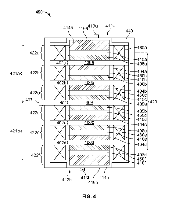
[0029] FIG. 4 shows a schematic cross-sectional view
of a structure of a stack of BPUs according to an
embodiment of the invention. As shown in FIG. 4, for
example, independent cell stacks or sub-stacks 421a
and 421b may be configured to be electrically coupled in
parallel by having a "sub-terminal" mono-polar electrode
unit located between the sub-stacks (see, e.g.,
sub-terminal MPU 401). Positive or negative sub-terminal
mono-polar electrode units (MPUs) may be provided between
independent cell stacks, or sub-stacks, in a bi-polar
ESD. The sub-terminal MPUs may have active material
electrode layers having the same polarity (i.e., positive
or negative) provided on opposite sides of a substrate or
current collector. Any suitable active material may be
used with sub-terminal MPUs, and in some embodiments the
active material electrode layers on either side of a
sub-terminal MPU may be substantially the same active
material or may be different active materials having the
same polarity.
[0030] For example, FIG. 4 shows sub-terminal MPU 401
within stack 420 of bi-polar ESD 450. Sub-terminal
CA 02759388 2011-10-20
WO 2010/124195 PCT/US2010/032216
- 9 -
MPU 401 may include a negative active material electrode
layer 405a that may be provided on a first side of an
impermeable conductive substrate or current
collector 409, and a negative active material electrode
layer 405b that may be provided on the other side of
impermeable conductive substrate 409. Sub-terminal
MPU 401 may be configured to electrically couple the cell
segments of sub-stack 421a (see, e.g., cell
segments 422a-422c) in parallel with the cell segments of
sub-stack 421b (see, e.g., cell segments 422d-422f). For
example, sub-terminal MPU 401 may be provided with a tab
or flange 407. In some embodiments, flange 407 may
provide, for example, an electrical connection to the
bi-polar electrode unit or mono-polar unit corresponding
to the respective substrate to which flange 407 is
attached. As shown in FIG. 4, for example, flange 407 is
attached to substrate 409 of sub-terminal MPU 401.
However, it will be understood that tabs or flanges may
be provided with the substrates of any suitable electrode
units of the present invention, including, for example,
the BPUs, sub-terminal MPUs, and terminal MPUs (see,
e.g., flanges 607 of FIGS. 6-9).
[0031] Sub-terminal MPU 401 may act as an electrical
separator, a mechanical separator, or both, between sub-
stacks. In some embodiments, sub-terminal MPU 401 may
have a different geometry than the bi-polar electrode
units (see, e.g., BPUs 402a-d). For example,
substrate 409 of sub-terminal MPU 401 may be relatively
thicker or relatively thinner than substrate 406a of
BPU 402a. Substrate 409 may be have variable thicknesses
CA 02759388 2011-10-20
WO 2010/124195 PCT/US2010/032216
- 10 -
relative to substrate 406a, for example, because the
electrodes having the same polarity on either side of
substrate 409 (e.g., electrode layers 405a and 405b) may
expand and/or contract differently than the electrodes on
either side of substrate 406a that have opposite
polarities (e.g., electrode layers 408a and 404a). For
example, if MPU 401 has positive electrode layers on
either side of substrate 409, one or both positive
electrode layers may compress substrate 409.
Furthermore, in some embodiments the sub-stacks of the
ESD may have different base units and/or different
chemistries (e.g., substack 421a may have a nickel-metal
hydride ESD chemistry and substack 421b may utilize
capacitors). In such embodiments, for example, the sub-
stacks may expand and/or contract differently relative to
one another, thereby exerting a net force on MPU 401.
Thus, in some embodiments substrate 409 may be designed
to be relatively thicker and more robust than
substrates 406a-d. It will be understood, however, that
in some embodiments, substrate 409 of sub-terminal
MPU 401 may be substantially the same as the
substrates of the BPUs (see, e.g., substrates 406a-d of
BPUs 402a-d).
[0032] Sub-terminal MPU 401 may have any suitable
inter-electrode spacing between the active materials of
adjacent cell segments and may have any suitable gasket
configuration. The inter-electrode spacing may depend on
various ESD applications. For example, for relatively
lower drain/high energy cells, it may be preferable to
pack a relatively greater quantity of active materials
CA 02759388 2011-10-20
WO 2010/124195 PCT/US2010/032216
- 11 -
and/or have a relatively thicker electrode matrix
material to withstand the increased loading. For
relatively higher power applications, it may be
preferable to pack less material and/or close at a
relatively higher force to decrease the inter-electrode
spacing.
[0033] There may be many criteria for ESD design.
These criteria typically specify power, energy, and
service life, and may have limitations for mass and/or
volume. These criteria may not be met by one ESD type
alone. Therefore, in some embodiments, ESDs that combine
energy storage types to achieve design requirements may
be preferred. The bi-polar ESD of the present invention
may be configured to accommodate multiple ESD types to
achieve design requirements. For example, as discussed
above, one sub-stack may have a nickel-metal hydride ESD
chemistry and another sub-stack may utilize capacitors.
[0034] Bi-polar ESD 450 may include one or more
fundamental base units. For example, suitable
electrochemical ESD chemistries may include metal
hydride, lithium, or any other suitable chemistry, or
combinations thereof, and base units may include
electrostatic capacitors. The multi-unit ESD may be
configured for series or parallel power distribution, or
both, and the device may include multiple types. In some
embodiments, independent sub-stacks within an ESD may
have different chemistries. For example, sub-stack 421a
may include metal hydride elements and sub-stack 421b may
include lithium-ion elements. In some embodiments, cells
CA 02759388 2011-10-20
WO 2010/124195 PCT/US2010/032216
- 12 -
within the same sub-stack may have different chemistries
from cell-to-cell or even within the same cell.
[0035] As discussed above, in some embodiments the ESD
may include one or more sub-stacks having capacitors
stacked therein. The capacitors may include an
electrochemical double layer. The double layer component
may refer to the accumulation of ions and electrons on
the surface of the electrode materials (e.g., they may be
contact surface area dependant). The effect may be
relatively more electrostatic than electrochemical as
ions and electrons may both be coupled on the surface of
the electrode materials. This may be similar, for
example, to electrostatic capacitors. The positive and
negative electrode layers of the capacitor may have
substantially the same composition so that there may be
no or substantially no "natural" electrochemical
potential when the ESD is assembled. The potential may
arise when the ESD is charged, for example, by having
electrons on one side and a substantially equal positive
ionic charge that accumulates on the same surface. A
similar event may occur on the negative electrode, for
example, where negative ions may accumulate on the
electrode surface caused by the depletion of electrons
(e.g., "holes") on the negative electrodes' electron
depleted surface. It will be understood that, as
discussed above in connection with the bi-polar units of
the present invention, either side of the capacitor may
be positive or negative.
[0036] When capacitors are electrically coupled in
parallel with an ESD, the overall assembly may have a
CA 02759388 2011-10-20
WO 2010/124195 PCT/US2010/032216
- 13 -
relatively higher working voltage. For example, metal
hydride ESDs may be aqueous and may have an operating
range of 1.5 volts. Capacitors having an electrochemical
double layer may be formed of any suitable electrolyte
and the operating ranges may be from 1.25 volts, or
lower, to 20 volts, or higher, for example. The
capacitors may also have a relatively low internal
resistance, and may support ESDs having relatively high
current draws. For example, for high-rate pulses, the
capacitors may take most of the current draw before the
ESD, which may buffer the ESD and which may increase the
cycle life of the ESD.
[0037] Other capacitors may not have a double layer of
ions and electrons. Rather, they may only operate via
the electrostatic couple caused by the accumulation and
depletion of electrons on the surface of the conductor
(e.g., on metal foils). Once charged, the electrons may
not propagate through the dielectric separator but may
require close proximity to hold the electrostatic couple.
Once the positive and negative terminals are coupled to
bridge the circuit, electrons may flow back across the
wires to re-equilibrate to substantially zero voltage.
These capacitors may have a capacity that is relatively
lower than capacitors having an electrochemical double
layer.
[0038] The number of capacitor cells stacked in a
sub-stack may depend on the voltage limits of the ESD.
In some embodiments, the voltage of the capacitor
sub-stack may be equal to or greater than the voltage of
the ESD. Moreover, in some embodiments, for example, the
CA 02759388 2011-10-20
WO 2010/124195 PCT/US2010/032216
- 14 -
voltage limit per cell of the capacitor may depend upon
the electrolyte solvent breakdown voltage. Exemplary
voltage limits may range from 1.2 volts (e.g., aqueous)
to 20 volts (e.g., organic and siloxane) for liquid-based
solvent devices. In some embodiments, the ESD of the
present invention may incorporate capacitors in a sub-
stack having substantially the same solvent as that used
in another sub-stack having, for example, metal hydride
chemistry, where the cells may be configured to have a
1.5 volt limit.
[0039] With continued reference to FIG. 4, there are
two independent three-cell stacks (i.e., sub-stacks 421a
and 421b) with sub-terminal MPU 401 thus centrally
located in stack 420 between sub-stacks 421a and 421b.
It will be understood, however, that sub-terminal MPU 401
may provided at any suitable location within stack 420.
For example, independent cell stacks (see, e.g.,
sub-stack 421a) may have any suitable number of cells
(e.g., to increase the voltage of a particular stack or
sub-stack) so that sub-terminal MPU 401 may be located in
any suitable location in a stack that is between the
independent sub-stacks (e.g., sub-stacks 421a and 421b).
It will also be understood that ESD 450 may have any
suitable number of independent cell stacks or sub-stacks,
with an appropriate number of sub-terminal MPUs provided
therebetween. In some embodiments, for example, multiple
sub-stacks may be incorporated to increase the voltage
and/or current capacity of the ESD.
[0040] As shown in FIG. 4, for example, positive or
negative terminals, or terminal mono-polar units (MPUs),
CA 02759388 2011-10-20
WO 2010/124195 PCT/US2010/032216
- 15 -
may be provided along with stack 420 of one or more
BPUs 402a-d and sub-terminal MPU 401 to constitute a
stacked bi-polar ESD 450 in accordance with an embodiment
of the invention. In the arrangement shown in FIG. 4,
for example, the polarity of the terminal MPUs may be
opposite the polarity of sub-terminal MPU 401. A
positive terminal MPU 412b, that may include a positive
active material electrode layer 414b provided on one side
of an impermeable conductive substrate 416b, may be
positioned at a first end of stack 420 with an
electrolyte layer provided (i.e., electrolyte
layer 410f), such that positive electrode layer 414b of
positive terminal MPU 412b may be opposed to a negative
electrode layer (i.e., layer 408d) of the BPU
(i.e., BPU 402d) at that first end of stack 420 via the
electrolyte layer 410f. A positive terminal MPU 412a,
that may include a positive active material electrode
layer 414a provided on one side of an impermeable
conductive substrate 416a, may be positioned at the
second end of stack 420 with an electrolyte layer
provided (i.e., electrolyte layer 410a), such that
positive electrode layer 414a of positive terminal
MPU 412a may be opposed to a negative electrode layer
(i.e., layer 408a) of the BPU (i.e., BPU 402a) at that
second end of stack 420 via the electrolyte layer 410a.
Terminal MPUs 412a and 412b may be provided with
corresponding positive electrode leads 413a and 413b,
respectively.
[0041] The substrate and electrode layer of each
terminal MPU or sub-terminal MPU may form a cell segment
CA 02759388 2011-10-20
WO 2010/124195 PCT/US2010/032216
- 16 -
with the substrate and electrode layer of its adjacent
BPU, and the electrolyte layer therebetween, as shown in
FIG. 4, for example (see, e.g., cell segments 422a/422f
and cell segments 422c/422d). The number of stacked BPUs
in stack 420 may be one or more, and may be appropriately
determined in order to correspond, for example, to a
desired voltage for ESD 450. The number of stacked BPUs
in a sub-stack (e.g., sub-stacks 421a and 421b) may be
one or more, and may be appropriately determined in order
to correspond, for example, to a desired voltage for
ESD 450. Each BPU may provide any desired potential,
such that a desired voltage for ESD 450 may be achieved
by effectively adding the potentials provided by each
component BPU. It will be understood that each BPU need
not provide identical potentials.
[0042] In one suitable embodiment, bi-polar ESD 450
may be structured so that BPU stack 420 and its
respective positive terminal MPUs 412a and 412b may be at
least partially encapsulated (e.g., hermetically sealed)
into an ESD case or wrapper 440 under reduced pressure.
Terminal MPU conductive substrates 416a and 416b (or at
least their respective electrode leads 413a and 413b) may
be drawn out of ESD case or wrapper 440, so as to
mitigate impacts from the exterior upon usage and to
prevent environmental degradation, for example.
[0043] In order to prevent electrolyte of a first cell
segment (see, e.g., electrolyte layer 410a of cell
segment 422a) from combining with the electrolyte of
another cell segment (see, e.g., electrolyte layer 410b
of cell segment 422b), gaskets or sealants may be stacked
CA 02759388 2011-10-20
WO 2010/124195 PCT/US2010/032216
- 17 -
with the electrolyte layers between adjacent electrode
units to seal electrolyte within its particular cell
segment. A gasket or sealant may be any suitable
compressible or incompressible solid or viscous material,
any other suitable material, or combinations thereof, for
example, that may be provided with adjacent electrode
units of a particular cell to seal electrolyte
therebetween. In one suitable arrangement, as shown in
FIG. 4, for example, the bi-polar ESD of the invention
may include gaskets or seals 460a-f that may be
positioned as a barrier about electrolyte layers 410a-f
and active material electrode layers 404a-d/414a-b
and 408a-d/405a-b of each cell segment 422a-e. The
gasket or sealant may be continuous and closed and may
seal electrolyte between the gasket and the adjacent
electrode units of that cell (i.e., the BPUs or the BPU
and sub-terminal MPU/terminal MPU adjacent to that gasket
or seal). The gasket or sealant may provide appropriate
spacing between the adjacent electrode units of that
cell, for example. In some embodiments a dynamic
flexible seal or gasket may be provided. In this
application the gasket may mechanically adjust dimensions
while maintaining a substantially sealed contact with the
adjoining surfaces. For example, the dynamic flexible
seal or gasket may be configured to deform in a preferred
direction or preferred directions. Dynamic flexible
seals and gaskets are discussed in more detail in West et
al. U.S. Patent Application No. 12/694,638, which is
hereby incorporated by reference herein in its entirety.
CA 02759388 2011-10-20
WO 2010/124195 PCT/US2010/032216
- 18 -
[0044] In sealing the cell segments of stacked
bi-polar ESD 450 to prevent electrolyte of a first cell
segment (see, e.g., electrolyte layer 410a of cell
segment 422a) from combining with the electrolyte of
another cell segment (see, e.g., electrolyte layer 410b
of cell segment 422b), cell segments may produce a
pressure differential between adjacent cells
(e.g., cells 422a/422b) as the cells are charged and
discharged. Equalization valves may be provided to
substantially decrease the pressure differences thus
arising. Equalization valves may operate as a semi-
permeable membrane or rupture disk, either mechanically
or chemically, to allow the transfer of a gas and to
substantially prevent the transfer of electrolyte. An
ESD may have BPUs, sub-terminal MPUs, and terminal MPUs
having any combination of equalization valves. Pressure
equalization valves are discussed in more detail in West
et. al U.S. Patent Application No. 12/258,854, which is
hereby incorporated by reference herein in its entirety.
[0045] FIG. 5 shows a schematic circuit diagram of the
bi-polar ESD of FIG. 4 according to an embodiment of the
invention. For example, the cell segments within each
respective independent cell stacks or sub-stack may be
electrically coupled in series with the other cells of
the sub-stack (see, e.g., the series-connection of
FIGS. 2 and 3). The two sub-stacks may then be
electrically coupled in parallel to one another via a
sub-terminal MPU (see, e.g., sub-terminal MPU 401 of
FIG. 4). This arrangement may allow, for example,
multiple cells to be electrically coupled in series
CA 02759388 2011-10-20
WO 2010/124195 PCT/US2010/032216
- 19 -
and/or in parallel in a stack while using only one pair
of end caps (see, e.g., end caps 618 and 634 of
FIGS. 6-8). This may reduce the parasitic weight of the
ESD compared to, for example, ESDs electrically coupled
in series and in parallel using multiple end caps.
[0046] As shown in FIG. 5, for example, the sub-stacks
may be electrically coupled in parallel via one or more
wires that may be attached to sub-terminal MPU 401. The
wires may be attached to one or more flanges of the
substrate of sub-terminal MPU 401 (see, e.g., flange 407
of FIG. 4 and flanges 607 of FIGS. 6-9). It will be
understood that utilizing a wire is only one of many
suitable approaches for making the parallel connections.
For example, in some embodiments a sub-terminal MPU may
be bonded directly to a conductive outside container
(see, e.g., ESD wrapper 440 of FIG. 4) and no wires may
be needed. In this embodiment, for example, each end of
the ESD may have both a positive post or electrode lead
(see, e.g., leads 413a and 413b) and a negative casing
(not shown) in contact with the conductive outside
container for providing a negative electrical connection.
Any other suitable approach for electrically coupling the
sub-stacks in parallel via sub-terminal MPU 401 may be
used, or any combinations thereof. For example, in some
embodiments both wires and a sub-terminal MPU bonded
directly to a conductive outside container may be used.
[0047] FIGS. 6 and 7 show a perspective view and a
partial cross-sectional view, respectively, of a stacked
bi-polar ESD according to an embodiment of the present
invention. Stacked bi-polar ESD 650 may include
CA 02759388 2011-10-20
WO 2010/124195 PCT/US2010/032216
- 20 -
compression bolts 623, alignment rings 624a and 624b,
mechanical springs 626a and 626b, stack 620 (including
substrate flanges 607), and rigid end caps 634 and 618
provided at either end of stack 620. Alignment rings may
be provided at either end of stacked bi-polar ESD 650.
For example, alignment ring 624a and alignment ring 624b
may be provided at opposing ends of ESD 650. Mechanical
springs may be provided between alignment rings 624a/624b
and rigid end caps 634/618. For example, mechanical
springs 626a may be provided between alignment ring 624a
and rigid end cap 634 and mechanical springs 626b may be
provided between alignment ring 624b and rigid end
cap 618. Mechanical springs 626a and 626b may be
configured to deflect in response to forces generated
during operation and cycling of ESD 650. In some
embodiments, deflection of springs 626a and 626b may be
directly proportional to the applied load.
[0048] Rigid end caps 634 and 618 may be shaped to
substantially conform to the shape of the electrodes
and/or substrates of bi-polar ESD 650 (see,
e.g., BPUs 402a-d of FIG. 4). For example, end caps 634
and 618 may conform to the "flat plate," "dish-shaped,"
or any other shape, or combinations thereof, of the
electrodes and/or substrates of ESD 350.
[0049] In some embodiments, substrate flanges 607 may
be provided about bi-polar ESD 650 and may extrude
radially outwardly from stack 620. Flange 607 may
provide, for example, an electrical connection to a
bi-polar electrode unit or mono-polar unit corresponding
to the respective impermeable conductive substrate to
CA 02759388 2011-10-20
WO 2010/124195 PCT/US2010/032216
- 21 -
which flange 607 is attached (see, e.g., flange 407 of
sub-terminal MPU 401 of FIG. 4). Although flange 607 of
FIG. 6 is shaped as a "tongue depressor," it may be any
other suitable shape, and of any other suitable size,
configured to extend radially outwardly from stack 620.
For example, the cross-sectional area of flange 607 may
be substantially rectangular, triangular, circular or
elliptical, hexagonal, or any other desired shape or
combination thereof, and may be configured to
electrically couple with a particular connector or
connectors.
[0050] FIGS. 8 and 9 show an exploded view of the
stacked bi-polar ESD of FIG. 6 according to an embodiment
of the invention. As shown in FIG. 8, for example,
stack 620 may include sub-stacks 621a and 621b.
Sub-stack 621a may include a stack of five BPUs 602a.
Similarly, sub-stack 621b may include a stack of five
BPUs 602b. It will be understood, however, that any
suitable number of cell segments and/or bi-polar units
may be provided in sub-stacks 621a and 621b to
correspond, for example, to a desired voltage and/or
current capacity for ESD 650. A sub-terminal MPU 601 may
be provided between sub-stacks 621a and 621b thereby
separating the series electrical connections of the BPUs
of sub-stack 621a from the series electrical connections
of the BPUs of sub-stack 621b. Sub-terminal MPU 601 may
be configured to couple the BPUs of sub-stack 621a in
parallel with the BPUs of sub-stack 621b, for example,
via the plurality of flanges 607 attached to each
respective substrate (see, e.g., flanges 607 of FIG. 9).
CA 02759388 2011-10-20
WO 2010/124195 PCT/US2010/032216
- 22 -
As discussed above in connection with FIG. 5, it will be
understood that utilizing flanges (e.g., flanges 607) is
only one of many suitable approaches for making the
parallel connections between sub-stacks of an ESD.
[0051] Referring to FIG. 9 (represented as region 690
of FIG. 8), sub-terminal MPU 601 may have active material
electrode layers having the same polarity (i.e., positive
or negative) provided on opposite sides of a substrate or
current collector. As shown in FIG. 9, for example,
sub-terminal MPU 601 may include a positive active
material electrode layer 603 that may be provided on a
first side of an impermeable conductive substrate or
current collector 609. A second positive active material
electrode layer may be provided on the other side of
impermeable conductive substrate 609 (not shown).
[0052] BPU 602a may include a positive active material
electrode layer 604 that may be provided on a first side
of an impermeable conductive substrate or current
collector 606, and a negative active material electrode
layer 608 (not shown) that may be provided on the other
side of impermeable conductive substrate 606. BPU 602b
may include a negative active material electrode
layer 608 that may be provided on a first side of
impermeable conductive substrate or current
collector 606, and a positive active material electrode
layer 604 (not shown) that may be provided on the other
side of impermeable conductive substrate 606. The
substrates 606 may further include substrate flanges 607
extending radially outwardly therefrom.
CA 02759388 2011-10-20
WO 2010/124195 PCT/US2010/032216
- 23 -
[0053] By separating the sub-stacks of ESD 650,
sub-terminal MPU 601 may in effect operate as an end cap
for a particular sub-stack. As shown in FIGS. 6-8, for
example, ESD 650 has at least two sub-stacks electrically
coupled in parallel and arranged in a single stack 620
having only one pair of end caps 618 and 634.
[0054] With continuing reference to FIG. 9, hard
stops 662 may be provided between each respective
electrode unit (e.g., BPUs 602a and 602b and sub-terminal
MPU 601). Hard stops 662 may substantially encircle the
contents of each respective cell segment. Furthermore,
each hard stop 662 may have a shelf on which a substrate
(e.g., substrates 606 and 609) may be securely
positioned.
[0055] A set of bolt holes 664 for a plurality of
compression bolts (see, e.g., compression bolts 623 of
FIG. 6), or any other suitable rigid fasteners, may be
provided along the outer rim of hard stops 662. Bolt
holes 664 may align an entire stack of electrode units
(see, e.g., BPUs 402a-d, sub-terminal MPU 401, and
terminal MPUs 412a and 412b) during assembly, for
example, and may provide stability during operation.
Bolt holes 664 may be sized to accommodate a particular
compression bolt or any other suitable rigid fastener.
While bolt holes 664 are shown as circular, they may also
be substantially rectangular, triangular, elliptical,
hexagonal, or any other desired shape or combination
thereof.
[0056] Hard stops 662 may also include a plurality of
substrate shelves 674 that may align with substrate
CA 02759388 2011-10-20
WO 2010/124195 PCT/US2010/032216
- 24 -
flanges 607. Substrate shelves 674 may allow a flange to
protrude radially outwardly from stack 620 through hard
stop 662 to allow the flange, for example, to
electrically couple to a lead. Although hard stops 662
are shown as each having five substrate shelves 674, any
suitable number of shelves 674 may be provided and that
number may depend on the particular electrode units used
in the ESD. Furthermore, the hard stops 662 may be
configured to substantially set the inter-electrode
spacing of the ESD. Various techniques for adjusting the
inter-electrode spacing of ESDs are described in more
detail in West et al. U.S. Patent Application
No. 12/694,638, which is hereby incorporated by reference
herein in its entirety.
[0057] The substrates used to form the electrode units
of the invention (e.g., substrates 406a-d, 409, 416a,
and 416b) may be formed of any suitable conductive and
impermeable or substantially impermeable material,
including, but not limited to, a non-perforated metal
foil, aluminum foil, stainless steel foil, cladding
material including nickel and aluminum, cladding material
including copper and aluminum, nickel plated steel,
nickel plated copper, nickel plated aluminum, gold,
silver, any other suitable material, or combinations
thereof, for example. Each substrate may be made of two
or more sheets of metal foils adhered to one another, in
certain embodiments. The substrate of each BPU may
typically be between 0.025 and 5 millimeters thick, while
the substrate of each MPU may be between 0.025 and 10
millimeters thick and act as terminals or sub-terminals
CA 02759388 2011-10-20
WO 2010/124195 PCT/US2010/032216
- 25 -
to the ESD, for example. Metalized foam, for example,
may be combined with any suitable substrate material in a
flat metal film or foil, for example, such that
resistance between active materials of a cell segment may
be reduced by expanding the conductive matrix throughout
the electrode.
[0058] In some embodiments, substrate 409 of
sub-terminal MPU 401 may be formed of any suitable
non-conductive and impermeable or substantially
impermeable material, including, but not limited to,
various plastics, phenolics, ceramics, epoxy performs in
a binary composite, glass-ceramics, multiple dimensional
woven fiber composites, any other suitable material, or
combinations thereof, for example.
[0059] The positive electrode layers provided on these
substrates to form the electrode units of the invention
(e.g., positive electrode layers 404a-d, 414a, and 414b)
may be formed of any suitable active material, including,
but not limited to, nickel hydroxide (Ni(OH)2), zinc (Zn),
any other suitable material, or combinations thereof, for
example. The positive active material may be sintered
and impregnated, coated with an aqueous binder and
pressed, coated with an organic binder and pressed, or
contained by any other suitable technique for containing
the positive active material with other supporting
chemicals in a conductive matrix. The positive electrode
layer of the electrode unit may have particles,
including, but not limited to, metal hydride (MH),
palladium (Pd), silver (Ag), any other suitable material,
or combinations thereof, infused in its matrix to reduce
CA 02759388 2011-10-20
WO 2010/124195 PCT/US2010/032216
- 26 -
swelling, for example. This may increase cycle life,
improve recombination, and reduce pressure within the
cell segment, for example. These particles, such as MH,
may also be in a bonding of the active material paste,
such as Ni(OH)2, to improve the electrical conductivity
within the electrode and to support recombination.
[0060] The negative electrode layers provided on these
substrates to form the electrode units of the invention
(e.g., negative electrode layers 408a-d, 405a, and 405b)
may be formed of any suitable active material, including,
but not limited to, MH, Cd, Mn, Ag, any other suitable
material, or combinations thereof, for example. The
negative active material may be sintered, coated with an
aqueous binder and pressed, coated with an organic binder
and pressed, or contained by any other suitable technique
for containing the negative active material with other
supporting chemicals in a conductive matrix, for example.
The negative electrode side may have chemicals including,
but not limited to, Ni, Zn, Al, any other suitable
material, or combinations thereof, infused within the
negative electrode material matrix to stabilize the
structure, reduce oxidation, and extend cycle life, for
example.
[0061] Various suitable binders, including, but not
limited to, organic carboxymethylcellulose (CMC) binder,
Creyton rubber, PTFE (Teflon), any other suitable
material, or combinations thereof, for example, may be
mixed with the active material layers to hold the layers
to their substrates. Ultra-still binders, such
CA 02759388 2011-10-20
WO 2010/124195 PCT/US2010/032216
- 27 -
as 200 ppi metal foam, may also be used with the stacked
ESD constructions of the invention.
[0062] The separator of each electrolyte layer of the
ESD of the invention may be formed of any suitable
material that electrically isolates its two adjacent
electrode units while allowing ionic transfer between
those electrode units. The separator may contain
cellulose super absorbers to improve filling and act as
an electrolyte reservoir to increase cycle life, wherein
the separator may be made of a polyabsorb diaper
material, for example. The separator may, thereby,
release previously absorbed electrolyte when charge is
applied to the ESD. In certain embodiments, the
separator may be of a lower density and thicker than
normal cells so that the inter-electrode spacing (IES)
may start higher than normal and be continually reduced
to maintain the capacity (or C-rate) of the ESD over its
life as well as to extend the life of the ESD.
[0063] The separator may be a relatively thin material
bonded to the surface of the active material on the
electrode units to reduce shorting and improve
recombination. This separator material may be sprayed
on, coated on, pressed on, or combinations thereof, for
example. The separator may have a recombination agent
attached thereto, in certain embodiments. This agent may
be infused within the structure of the separator
(e.g., this may be done by physically trapping the agent
in a wet process using a polyvinyl alcohol (PVA or PVOH)
to bind the agent to the separator fibers, or the agent
may be put therein by electro-deposition), or it may be
CA 02759388 2011-10-20
WO 2010/124195 PCT/US2010/032216
- 28 -
layered on the surface by vapor deposition, for example.
The separator may be made of any suitable material or
agent that effectively supports recombination, including,
but not limited to, Pb, Ag, any other suitable material,
or combinations thereof, for example. While the
separator may present a resistance if the substrates of a
cell move toward each other, a separator may not be
provided in certain embodiments of the invention that may
utilize substrates stiff enough not to deflect.
[0064] The electrolyte of each electrolyte layer of
the ESD of the invention may be formed of any suitable
chemical compound that may ionize when dissolved or
molten to produce an electrically conductive medium. The
electrolyte may be a standard electrolyte of any suitable
chemical, including, but not limited to, NiMH, for
example. The electrolyte may contain additional
chemicals, including, but not limited to, lithium
hydroxide (LiOH), sodium hydroxide (NaOH), calcium
hydroxide (CaOH), potassium hydroxide (KOH), any other
suitable material, or combinations thereof, for example.
The electrolyte may also contain additives to improve
recombination, including, but not limited to, Ag(OH)2, for
example. The electrolyte may also contain rubidium
hydroxide (RbOH), for example, to improve low temperature
performance. In some embodiments of the invention, the
electrolyte may be frozen within the separator and then
thawed after the ESD is completely assembled. This may
allow for particularly viscous electrolytes to be
inserted into the electrode unit stack of the ESD before
CA 02759388 2011-10-20
WO 2010/124195 PCT/US2010/032216
- 29 -
the gaskets have formed substantially fluid tight seals
with the electrode units adjacent thereto.
[0065] The seals or gaskets of the ESD of the
invention (e.g., gaskets 460a-f) may be formed of any
suitable material or combination of materials that may
effectively seal an electrolyte within the space defined
by the gasket and the electrode units adjacent thereto.
In certain embodiments, the gasket may be formed from a
solid seal barrier or loop, or multiple loop portions
capable of forming a solid seal loop, that may be made of
any suitable nonconductive material, including, but not
limited to, nylon, polypropylene, cell gard, rubber,
PVOH, any other suitable material, or combinations
thereof, for example. A gasket formed from a solid seal
barrier may contact a portion of an adjacent electrode to
create a seal therebetween.
[0066] Alternatively or additionally, the gasket may
be formed from any suitable viscous material or paste,
including, but not limited to, epoxy, brea tar,
electrolyte (e.g., KOH) impervious glue, compressible
adhesives (e.g., two-part polymers, such as Loctite(D
brand adhesives made available by the Henkel Corporation,
that may be formed from silicon, acrylic, and/or fiber
reinforced plastics (FRPs) and that may be impervious to
electrolytes), any other suitable material, or
combinations thereof, for example. A gasket formed from
a viscous material may contact a portion of an adjacent
electrode to create a seal therebetween. In some
embodiments, a gasket may be formed by a combination of a
solid seal loop and a viscous material, such that the
CA 02759388 2011-10-20
WO 2010/124195 PCT/US2010/032216
- 30 -
viscous material may improve sealing between the solid
seal loop and an adjacent electrode unit. Alternatively
or additionally, an electrode unit itself may be treated
with viscous material before a solid seal loop, a solid
seal loop treated with additional viscous material, an
adjacent electrode unit, or an adjacent electrode unit
treated with additional viscous material, is sealed
thereto, for example.
[0067] Moreover, in certain embodiments, a gasket or
sealant between adjacent electrode units may be provided
with one or more weak points that may allow certain types
of fluids (i.e., certain liquids or gasses) to escape
therethrough (e.g., if the internal pressures in the cell
segment defined by that gasket increases past a certain
threshold). Once a certain amount of fluid escapes or
the internal pressure decreases, the weak point may
reseal. A gasket formed at least partially by certain
types of suitable viscous material or paste, such as
brai, may be configured or prepared to allow certain
fluids to pass therethrough and configured or prepared to
prevent other certain fluids to pass therethrough. Such
a gasket may prevent any electrolyte from being shared
between two cell segments that may cause the voltage and
energy of the ESD to fade (i.e., discharge) quickly to
zero.
[0068] As mentioned above, one benefit of utilizing
ESDs designed with sealed cells in a stacked formation
(e.g., bi-polar ESD 450) may be an increased discharge
rate of the ESD. This increased discharge rate may allow
for the use of certain less-corrosive electrolytes
CA 02759388 2011-10-20
WO 2010/124195 PCT/US2010/032216
- 31 -
(e.g., by removing or reducing the whetting, conductivity
enhancing, and/or chemically reactive component or
components of the electrolyte) that otherwise might not
be feasible in prismatic or wound ESD designs. This
leeway that may be provided by the stacked ESD design to
use less-corrosive electrolytes may allow for certain
epoxies (e.g., J-B Weld epoxy) to be utilized when
forming a seal with gaskets that may otherwise be
corroded by more-corrosive electrolytes.
[0069] The hard stops of the ESD of the invention
(see, e.g., hard stops 662 of FIG. 9) may be formed of
any suitable material including, but not limited to,
various polymers (e.g., polyethylene, polypropylene),
ceramics (e.g., alumina, silica), any other suitable
mechanically durable and/or chemically inert material, or
combinations thereof. The hard stop material or
materials may be selected, for example, to withstand
various ESD chemistries that may be used.
[0070] The mechanical springs of the invention (see,
e.g., mechanical springs 626a and 626b of FIGS. 6-8) may
be any suitable spring that may deflect or deform in
response to an applied load. For example, the mechanical
springs may be designed to deflect in response to
particular loads or a particular load threshold. Any
suitable type of spring may be used, including
compressible springs, such as open-coiled helical
springs, variable pitch springs, and torsion springs; or
flat springs, or any other suitable spring, or
combinations thereof. The spring itself may be any
suitable material, including, but not limited to, high
CA 02759388 2011-10-20
WO 2010/124195 PCT/US2010/032216
- 32 -
carbon steels, alloy steels, stainless steel, copper
alloys, any other suitable inflexible or flexible
material, or combinations thereof.
[0071] The end caps of the present invention (see,
e.g., end caps 618 and 636 of FIGS. 6-8) may be formed of
any suitable material or combination of materials that
may be conductive or non-conductive, including, but not
limited to various metals (e.g., steel, aluminum, and
copper alloys), polymers, ceramics, any other suitable
conductive or non-conductive material, or combinations
thereof.
[0072] A case or wrapper of the ESD of the invention
(see, e.g., wrapper 440 of FIG. 4) may be provided, and
may be formed of any suitable nonconductive material that
may seal to the terminal electrode units (e.g., terminal
MPUs 412a and 412b) for exposing their conductive
substrates (e.g., substrates 416a and 416b) or their
associated leads (e.g., leads 413a and 413b). The
wrapper may also be formed to create, support, and/or
maintain the seals between the gaskets and the electrode
units adjacent thereto for isolating the electrolytes
within their respective cell segments. The wrapper may
create and/or maintain the support needed for these seals
such that the seals may resist expansion of the ESD as
the internal pressures in the cell segments increase.
The wrapper may be made of any suitable material,
including, but not limited to, nylon, any other polymer
or elastic material, including reinforced composites,
nitrile rubber, or polysulfone, or shrink wrap material,
or any rigid material, such as enamel coated steel or any
CA 02759388 2011-10-20
WO 2010/124195 PCT/US2010/032216
- 33 -
other metal, or any insulating material, any other
suitable material, or combinations thereof, for example.
In certain embodiments, the wrapper may be formed by an
exoskeleton of tension clips, for example, that may
maintain continuous pressure on the seals of the stacked
cells. A non-conductive barrier may be provided between
the stack and wrapper to prevent the ESD from shorting.
[0073] With continued reference to FIG. 4, for
example, bi-polar ESD 450 of the invention may include a
plurality of cell segments (e.g., cell segments 422a-f)
formed by terminal MPUs 412a and 412b, and the sub-stacks
of one or more BPUs 402a-d having sub-terminal MPU 401
therebetween. In accordance with an embodiment of the
invention, the thicknesses and materials of each one of
the substrates (e.g., substrates 406a-d, 409, 416a,
and 416b), the electrode layers (e.g., positive
layers 404a-d, 414a, and 414b, and negative
layers 408a-d, 405a, and 405b), the electrolyte layers
(e.g., layers 410a-f), and the gaskets
(e.g., gaskets 460a-f) may differ from one another, not
only from cell segment to cell segment, but also within a
particular cell segment. This variation of geometries
and chemistries, not only at the stack level, but also at
the individual cell level, may create ESDs with various
benefits and performance characteristics.
[0074] Additionally, the materials and geometries of
the substrates, electrode layers, electrolyte layers, and
gaskets may vary along the height of the stack from cell
segment to cell segment. With further reference to
FIG. 4, for example, the electrolyte used in each of the
CA 02759388 2011-10-20
WO 2010/124195 PCT/US2010/032216
- 34 -
electrolyte layers 410a-f of ESD 450 may vary based upon
how close its respective cell segment 422a-f is to the
middle of the stack or sub-stack of cell segments. For
example, with reference to sub-stack 421a, innermost cell
segment 422b (i.e., the middle cell segment of the
three (3) segments) may include an electrolyte layer
(i.e., electrolyte layer 410b) that is formed of a first
electrolyte, while outermost cell segments 422a and 422c
(i.e., the outermost cell segments in sub-stack 421a) may
include electrolyte layers (i.e., electrolyte layers 410a
and 410b, respectively) that are each formed of a second
electrolyte. By using higher conductivity electrolytes
in the internal sub-stacks, the resistance may be lower
such that the heat generated may be less. This may
provide thermal control to the ESD by design instead of
by external cooling techniques.
[0075] As another example, the active materials used
as electrode layers in each of the cell segments of
ESD 450 may also vary based upon how close its respective
cell segment 422a-f is to the middle of the stack or
sub-stack of cell segments. For example, with reference
to sub-stack 421a, innermost cell segment 422b may
include electrode layers (i.e., layers 404a and 408b)
formed of a first type of active materials having a first
temperature and/or rate performance, while outermost cell
segments 422a and 422c may include electrode layers
(i.e., layers 414a/408a and layers 404b/405a) formed of a
second type of active materials having a second
temperature and/or rate performance. As an example, an
ESD stack may be thermally managed by constructing the
CA 02759388 2011-10-20
WO 2010/124195 PCT/US2010/032216
- 35 -
innermost cell segments with electrodes of nickel
cadmium, which may better absorb heat, while the
outermost cell segments may be provided with electrodes
of nickel metal hydride, which may need to be cooler, for
example. Alternatively, the chemistries or geometries of
the ESD may be asymmetric, where the cell segments at one
end of the stack may be made of a first active material
and a first height, while the cell segments at the other
end of the stack may be of a second active material and a
second height.
[0076] Moreover, the geometries of each of the cell
segments of ESD 450 may also vary along the stack of cell
segments. Besides varying the distance between active
materials within a particular cell segment, certain cell
segments 422a-f may have a first distance between the
active materials of those segments, while other cell
segments may have a second distance between the active
materials of those segments. In any event, the cell
segments or portions thereof having smaller distances
between active material electrode layers may have higher
power, for example, while the cell segments or portions
thereof having larger distances between active material
electrode layers may have more room for dendrite growth,
longer cycle life, and/or more electrolyte reserve, for
example. These portions with larger distances between
active material electrode layers may regulate the charge
acceptance of the ESD to ensure that the portions with
smaller distances between active material electrode
layers may charge first, for example.
CA 02759388 2011-10-20
WO 2010/124195 PCT/US2010/032216
- 36 -
[0077] In an embodiment, the geometries of the
electrode layers (e.g., positive layers 404a-d, 414a, and
414b, and negative layers 408a-d, 405a, and 405b of
FIG. 4) of ESD 450 may vary along the radial length of
the substrates (e.g., substrates 406a-d, 409, 416a, and
416b). With respect to FIG. 4, the electrode layers are
of uniform thickness and are symmetric about the
electrode shape. In an embodiment, the electrode layers
may be non-uniform. For example, the positive active
material electrode layer and negative active material
electrode layer thicknesses may vary with radial position
on the surface of the conductive substrate. Non-uniform
electrode layers are discussed in more detail in West
et al. U.S. Patent Application No. 12/258,854, which is
hereby incorporated by reference herein in its entirety.
[0078] Although each of the above described and
illustrated embodiments of a stacked ESD show a cell
segment including a gasket sealed to each of a first and
second electrode unit for sealing an electrolyte therein,
it should be noted that each electrode unit of a cell
segment may be sealed to its own gasket, and the gaskets
of two adjacent electrodes may then be sealed to each
other for creating the sealed cell segment.
[0079] In certain embodiments, a gasket may be
injection molded to an electrode unit or another gasket
such that they may be fused together to create a seal.
In certain embodiments, a gasket may be ultrasonically
welded to an electrode unit or another gasket such that
they may together form a seal. In other embodiments, a
gasket may be thermally fused to an electrode unit or
CA 02759388 2011-10-20
WO 2010/124195 PCT/US2010/032216
- 37 -
another gasket, or through heat flow, whereby a gasket or
electrode unit may be heated to melt into an other gasket
or electrode unit. Moreover, in certain embodiments,
instead of or in addition to creating groove shaped
portions in surfaces of gaskets and/or electrode units to
create a seal, a gasket and/or electrode unit may be
perforated or have one or more holes running through one
or more portions thereof. Alternatively, a hole or
passageway or perforation may be provided through a
portion of a gasket such that a portion of an electrode
unit (e.g., a substrate) may mold to and through the
gasket. In yet other embodiments, holes may be made
through both the gasket and electrode unit, such that
each of the gasket and electrode unit may mold to and
through the other of the gasket and electrode unit, for
example.
[0080] Although each of the above described and
illustrated embodiments of the stacked ESD show an ESD
formed by stacking substrates having substantially round
cross-sections into a cylindrical ESD, it should be noted
that any of a wide variety of shapes may be utilized to
form the substrates of the stacked ESD of the invention.
For example, the stacked ESD of the invention may be
formed by stacking electrode units having substrates with
cross-sectional areas that are rectangular, triangular,
hexagonal, or any other desired shape or combination
thereof.
[0081] It will be understood that the foregoing is
only illustrative of the principles of the invention, and
that various modifications may be made by those skilled
CA 02759388 2011-10-20
WO 2010/124195 PCT/US2010/032216
- 38 -
in the art without departing from the scope and spirit of
the invention. It will also be understood that various
directional and orientational terms such as "horizontal"
and "vertical," "top" and "bottom" and "side," "length"
and "width" and "height" and "thickness," "inner" and
"outer," "internal" and "external," and the like are used
herein only for convenience, and that no fixed or
absolute directional or orientational limitations are
intended by the use of these words. For example, the
devices of this invention, as well as their individual
components, may have any desired orientation. If
reoriented, different directional or orientational terms
may need to be used in their description, but that will
not alter their fundamental nature as within the scope
and spirit of this invention. Those skilled in the art
will appreciate that the invention may be practiced by
other than the described embodiments, which are presented
for purposes of illustration rather than of limitation,
and the invention is limited only by the claims that
follow.