Note : Les descriptions sont présentées dans la langue officielle dans laquelle elles ont été soumises.
CA 02759432 2011-11-24
244587
SYSTEMS, METHODS, AND APPARATUS FOR LEAKAGE CURRENT
MASKING AND GROUND FAULT DETECTION
BACKGROUND OF THE INVENTION
The embodiments described herein relate generally to circuit fault detection
and, more
particularly, to detecting a ground fault in a circuit.
In a conventional electrical system, analysis of sinusoidal AC current and
voltage
performance is simplified by using a phasor characterization of the sinusoids.
Such
phasor characterizations generally use complex numbers having "real"
components
associated with resistive elements and "imaginary" components associated with
reactive
elements. For example, a phasor characterization of a ground fault current in
a circuit
includes a reactive, imaginary current component that flows through the
capacitive
elements of the electrical system, and a resistive, real current component.
The reactive
current component is purely reactive and neither causes heating nor presents a
shock
hazard. Therefore, the reactive current component of the ground fault current
does not
necessitate tripping of a protective device. In contrast, the resistive
component can cause
heating and present a shock hazard. Accordingly, only the resistive of the
ground fault
current necessitates tripping of the protective device.
At least some known systems and devices for use in charging an electric
device, such as
an electric vehicle or hybrid-electric vehicle, are incapable of
discriminating between
capacitive-generated leakage current and resistive ground current.
Accordingly, at least
some known systems and devices are susceptible to nuisance tripping, which
interrupts
current flow to the electric device. For example, a charging system or device
generally
connects to a power distribution network through a household wall power
outlet, such as
an outlet that is provided in a garage or carport. Most fire codes and
regulations require
1
CA 02759432 2011-11-24
244587
these outlets to include a ground fault circuit interrupt (GFCI) breaker or to
use a self-
contained ground fault interrupt wall outlet that detects resistive current.
However, many
electric vehicle on-board battery chargers generate a high leakage current
that can cause a
GFCI device, such as a GFCI breaker or a GFI wall outlet, to trip due to a
capacitive
current and when a true resistive ground fault is not actually present. At
least some GFCI
devices can be made to nuisance trip by a capacitive current to ground in the
absence of a
real, or resistive, ground fault condition. For example, the capacitive
current can exceed
a predetermined current threshold of at least some known GFCI devices and
result in a
nuisance trip of the GFCI device.
BRIEF DESCRIPTION OF THE INVENTION
In one aspect, a leakage current masking device is provided for use with a
circuit. The
leakage current masking device includes at least one inductive load device
coupled to the
circuit and configured to supply an inductive load to the circuit, and a
processor
communicatively coupled to the inductive load device. The processor is
configured to
receive a signal representative of a current through the circuit, calculate a
capacitive
leakage current component of the current, and cause the inductive load device
to adjust
the inductive load supplied to the circuit to reduce the capacitive leakage
current
component.
In another aspect, a charging system includes a ground fault circuit
interrupter (GFCI)
configured to detect a resistive ground fault in a circuit that couples a
source and a load,
and a leakage current masking device electrically coupled to the GFCI. The
leakage
current masking device includes at least one inductive load device coupled to
the circuit
and configured to supply an inductive load to the circuit, and a processor
communicatively coupled to the inductive load device. The processor is
configured to
receive a signal representative of a current through the circuit, calculate a
capacitive
leakage current component of the current, and cause the inductive load device
to adjust
the inductive load supplied to the circuit to reduce the capacitive leakage
current
component.
2
CA 02759432 2011-11-24
244587
In another aspect, a method is provided for detecting a resistive ground fault
in a circuit.
The method includes receiving at a processor a signal representative of a
current through
the circuit, and calculating a capacitive leakage current component and a
ground fault
current component of the current. The method also includes causing at least
one
inductive load device to adjust an inductive load supplied to the circuit to
reduce the
capacitive leakage current component, and detecting a resistive ground fault
in the circuit
based on the ground fault current component.
BRIEF DESCRIPTION OF THE DRAWINGS
Fig. 1 is a schematic block diagram of an exemplary charging system.
Fig. 2 is a schematic block diagram of an exemplary leakage current masking
device that
may be used with the charging system shown in Fig. 1.
Fig. 3 is a flowchart illustrating an exemplary method for detecting a
resistive ground
fault in a circuit using the charging system shown in Fig. 1.
DETAILED DESCRIPTION OF THE INVENTION
Exemplary embodiments of systems, methods, and apparatus for use in masking a
leakage current, such as a capacitive leakage current, and/or detecting a
ground fault are
described herein. These embodiments facilitate discriminating between
capacitive-
generated leakage current and resistive ground faults, thereby reducing
nuisance tripping
of circuit interruption devices, such as ground fault circuit interrupters.
The term "electric device" refers generally to any device that is capable of
receiving
power from an electrical outlet and storing at least a portion of that power
in a battery or
other electrical power storage device. Exemplary electric devices may include,
but are
not limited to only including, electrical vehicles and electric-hybrid
vehicles. The above
examples are exemplary only, and thus are not intended to limit in any way the
definition
and/or meaning of the term "electric device."
3
CA 02759432 2011-11-24
244587
Fig. 1 is a schematic block diagram of an exemplary charging system 100 for
use in
charging an electric device 102. In an exemplary embodiment, electric device
102
includes a charging device 104 and one or more batteries 106 that are
electrically coupled
to charging device 104. As described herein, electric device 102, charging
device 104,
and/or battery 106 may be referred to as a load.
In an exemplary embodiment, charging system 100 includes a power source 108, a
ground fault circuit interrupter (GFCI) 110, and a leakage current masking
device 200.
Masking device 200 is configured to be removably coupled between GFCI 110 and
charging device 104. In an alternative embodiment, masking device 200 is a
component
of electric device 102. For example, masking device 200 may be a component of
charging device 104 or may be electrically coupled to charging device 104.
Moreover, in an exemplary embodiment, masking device 200 adjusts an inductive
load
on a circuit or a portion of a circuit, such as a line conductor, until a
capacitive leakage
current flowing to ground is less than a predetermined threshold value or is
approximately cancelled. The threshold value can be any desired value. For
example, in
some applications the threshold value may be approximately five milliamps and,
thus, the
threshold value for capacitive leakage current should be lower. Preferably,
masking
device 200 adjusts the inductive load until the capacitive leakage current is
as close to
zero as possible. Once the inductive load is added to the circuit to reduce
the capacitive
leakage current, the circuit can be monitored for a resistive ground fault by
GFCI 110.
Reducing or cancelling the capacitive leakage current and measuring only a
resistive
current facilitates reducing nuisance trips of GFCI 110.
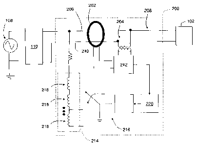
Fig. 2 is a schematic block diagram of leakage current masking device 200. In
an
exemplary embodiment, masking device 200 includes one or more current sensors
202
and one or more voltage sensors 204. Current sensor 202 measures a current,
such as a
residual current or a differential current, between GFCI 110 and the load. For
example,
current sensor 202 may measure the current through a phase or line conductor
206 of a
circuit 208. In an alternative embodiment, current sensor 202 measures a first
current
4
CA 02759432 2011-11-24
244587
through line conductor 206 and a second current through a neutral conductor
210 of
circuit 208. The residual current can then be calculated as a difference
between the first
current and the second current. In another alternative embodiment, and when
circuit 208
includes two line conductors 206, current sensor 202 measures a first current
through a
first line conductor, a second current through a second line conductor, and a
third current
through a neutral conductor 210. The residual current can then be calculated
as a sum of
the first and second currents, the second and third currents, or the first and
third currents.
In an exemplary embodiment, current sensor 202 is a current transformer.
However, any
suitable current sensor may be used that enables measurement of the current
through
circuit 208. Once the current is measured, current sensor 202 transmits a
signal
representative of the measured current. In an exemplary embodiment, voltage
sensor 204
measures a voltage between conductors of circuit 208. For example, voltage
sensor 204
may measure a voltage across line conductor 206 and neutral conductor 210. In
an
alternative embodiment, voltage sensor 204 measures a voltage across two line
conductors 206. Once the voltage is measured, voltage sensor 204 generates a
signal
representative of the measured voltage.
In an exemplary embodiment, masking device 200 also includes a signal
conditioning
unit 212 that is communicatively coupled to current sensor 202 and/or voltage
sensor
204. Signal conditioning unit 212 includes electrical components for use in,
for example
and not by way of limitation, filtering, amplifying, and/or converting the
current and/or
voltage signals. In an exemplary embodiment, signal conditioning unit 212
includes
analog-to-digital (A/D) converters (not shown) that convert an analog signal,
such as the
current signal and/or the voltage signal, to a digital signal using an A/D
conversion
operation.
Moreover, masking device 200 includes an inductive load device 214 and a
selector 216
that is operatively coupled to inductive load device 214. In an exemplary
embodiment,
inductive load device 214 includes an inductor with a plurality of taps 218
that enable
adjustment of the inductance of the inductor. Selector 216 is a switch that
selectively
CA 02759432 2011-11-24
244587
couples to a tap 218 of the inductor to adjust the amount of inductive load on
circuit 208.
In an alternative embodiment in which circuit 208 includes two line conductors
206 and
neutral conductor, masking device 200 includes multiple inductive load devices
214. In
such an embodiment, each inductive load device 214 provides an inductive load
to a
respective line conductor 206.
Furthermore, masking device 200 includes a processor 220 that is
communicatively
coupled to signal conditioning unit 212. The term "processor" refers generally
to any
programmable system including systems and microcontrollers, reduced
instruction set
circuits (RISC), application specific integrated circuits (ASIC), programmable
logic
circuits (PLC), and any other circuit capable of executing the functions
described herein.
The above examples are exemplary only, and thus are not intended to limit in
any way the
definition and/or meaning of the term "processor." In an exemplary embodiment,
processor 220 receives the current signal and/or the voltage signal from
current sensor
202 and/or voltage sensor 204, respectively. Specifically, processor 220
receives a
digitized current signal and/or a digitized voltage signal from signal
conditioning unit
212. Processor 220 then determines a real portion of the current signal and an
imaginary
portion of the current signal. In an exemplary embodiment, the real portion of
the current
signal represents a resistive ground fault current component and the imaginary
portion
represents a capacitive leakage current component. It should be understood
that, for a
given circuit having a ground fault current Igf, the current Igf can be
determined using a
ratio of the real portion of the product of the residual current Iõ which is
the sum of a
phase current and a neutral current, and a complex conjugate of phase to
neutral voltage
V. This is expressed in Equation (1) below:
Re I(',. X MI Eq. (1)
I
Moreover, when calculating the real and imaginary portions of the residual
current,
processor 220 produces a phasor representation of the line voltage by
multiplying the
measured line voltage by a first and a second predetermined sinusoidal
waveform. The
6
CA 02759432 2011-11-24
244587 '
first predetermined sinusoidal waveform is used to generate a real portion of
the line
voltage, and the second predetermined sinusoidal waveform is used to generate
an
imaginary portion of the line voltage. In some embodiments, the first and
second
sinusoidal waveforms are selected to match a frequency of the voltage of the
circuit. In
an exemplary embodiment, processor 220 then produces a phasor representation
of the
residual current by multiplying the measured or calculated residual current by
a third and
a fourth predetermined sinusoidal waveform. The third predetermined sinusoidal
waveform is used to generate the real portion of the residual current (i.e.,
the ground fault
current), and the fourth predetermined sinusoidal waveform is used to generate
the
imaginary portion of the residual current (i.e., the capacitive leakage
current). In some
embodiments, the third and fourth sinusoidal waveforms are selected to match a
frequency of the current of the circuit.
Based on the magnitude of the capacitive leakage current, processor 220
determines
whether an additional inductive load is necessary on circuit 208. Processor
220
determines an amount of inductive load to be added and causes selector 216 to
adjust the
inductive load on circuit 208 using inductive load device 214. For example,
processor
220 calculates a capacitance C using the capacitive leakage current I, the
line voltage V,
and a system frequency f. This calculation is illustrated by Equation (2)
below:
C _ 1,
V * 27r * f Eq. (2)
Processor 220 compares the capacitive leakage current to a threshold value. If
the
capacitive leakage current is greater than the threshold value, processor 220
transmits a
command signal to selector 216 to facilitate reducing the capacitive leakage
current
flowing to ground is less than the threshold value or is approximately
cancelled. In
response to the signal, selector 216 controls inductive load device 214 to
adjust the
inductive load on circuit 208, such as by increasing the inductive load. In an
exemplary
embodiment, the inductive load is based on the capacitance C of circuit 208
and the
7
CA 02759432 2011-11-24
244587
resonant frequency f of circuit 208. The resonant frequency f, of circuit 208
is calculated
by processor 220 using Equation (3) as shown below:
1 Eq. (3)
f r 27r LC
After the capacitive leakage current is appropriately reduced, processor 220
calculates a
magnitude of the line voltage phasor, and generates a complex conjugate of the
line
voltage phasor by determining a negative of the imaginary portion of the line
voltage.
The residual current phasor is then multiplied by the conjugate voltage phasor
to generate
a phasor representation of the ground fault current. The ground fault current
phasor is
calculated by dividing a magnitude of the line voltage phasor to obtain the
real portion of
the ground fault current. The Processor 220 then transmits the real portion of
the
ground fault current to GFCI 110.
GFCI 110 then determines if a true ground fault condition is present in
circuit 208. For
example, GFCI 110 compares the real portion of the ground fault current to a
threshold
value or predetermined level of ground fault current. If the real portion of
the ground
fault current is greater than the threshold value or predetermined level of
ground fault
current, then a true ground fault is determined to exist. In response to such
a
determination, GFCI 110 initiates opening circuit 208 by, for example,
tripping a circuit
breaker to remove the ground fault detection.
Fig. 3 is a flowchart 300 that illustrates an exemplary method for detecting a
resistive
ground fault in a circuit, such as circuit 208 (shown in Fig. 2). In an
exemplary
embodiment, current sensor 202 (shown in Fig. 2) measures 302 a current, such
as a
residual current, through a conductor of circuit 208. In some embodiments,
current
sensor 202 measures a first current through line conductor 206 (shown in Fig.
2),
measures a second current through neutral conductor 210 (shown in Fig. 2), and
transmits
first and second signals representative of the first and second currents,
respectively. In
addition, voltage sensor 204 (shown in Fig. 2) measures a voltage across
conductors of
8
CA 02759432 2011-11-24
244587
circuit 208, such as across line conductor 206 and neutral conductor 210.
Voltage sensor
204 transmits a third signal representative of the voltage. In an exemplary
embodiment,
signal conditioning unit 212 (shown in Fig. 2) receives the signals
representative of the
first current, the second current, and the voltage, and performs one or more
of a filtering
operation, an amplification operation, and an A/D conversion on the signals.
Signal
conditioning unit 212 then transmits 304 the signals to processor 220 (shown
in Fig. 2).
Processor 220 receives the signals and determines whether an inductive load on
circuit
208 should be adjusted and whether a ground fault current is present on
circuit 208.
Specifically, processor 220 calculates 306 a capacitive leakage current
component of the
residual current and a ground fault current component of the residual current.
For
example, as described in greater detail above, processor 220 calculates an
imaginary
portion of the residual current, which represents the capacitive leakage
current
component. Moreover, processor 220 calculates a real portion of the residual
current,
which represents the ground fault current component. Processor 220 compares
308 the
capacitive leakage current component to a first threshold value. Based on the
comparison, processor 220 determines 310 whether the capacitive leakage
current
component is greater than the first threshold value. If the capacitive leakage
current
component is not greater than the first threshold value, processor 220 waits
for a next
residual current signal to be transmit by signal conditioning unit 212. When
the
capacitive leakage current component is greater than the threshold value,
processor 220
calculates 312 an amount of inductive load to be added to circuit 208 to
approximately
cancel the capacitive leakage current component. Processor 220 transmits a
command
signal to selector 216 (shown in Fig. 2) that includes an amount of inductive
load to be
added to circuit 208 to approximately cancel the capacitive leakage current
component.
In response to the command signal, selector 216 causes inductive load device
214 (shown
in Fig. 2) to adjust the inductive load.
When the capacitive leakage current component has been approximately cancelled
or is at
least less than the first threshold value, processor 220 transmits a signal
representative of
9
CA 02759432 2011-11-24
244587
the ground fault current component to GFCI 110 (shown in Fig. 2). GFCI 110
compares
314 the ground fault current component to a second threshold to determine 316
whether a
ground fault is present on circuit 208. If a ground fault is present, GFCI 110
interrupts
318 current flow through circuit 208.
Exemplary embodiments of systems, methods, and apparatus for detecting a
ground fault
and/or masking a leakage current are described above in detail. The systems,
methods,
and apparatus are not limited to the specific embodiments described herein
but, rather,
operations of the methods and/or components of the systems and/or apparatus
may be
utilized independently and separately from other operations and/or components
described
herein. Further, the described operations and/or components may also be
defined in, or
used in combination with, other systems, methods, and/or apparatus, and are
not limited
to practice with only the systems, methods, and apparatus as described herein.
Although the present invention is described in connection with an exemplary
power
distribution system environment, embodiments of the invention are operational
with
numerous other general purpose or special purpose power distribution system
environments or configurations. The power distribution system environment is
not
intended to suggest any limitation as to the scope of use or functionality of
any aspect of
the invention. Moreover, the power distribution system environment should not
be
interpreted as having any dependency or requirement relating to any one or
combination
of components illustrated in an exemplary operating environment.
The order of execution or performance of the operations in the embodiments of
the
invention illustrated and described herein is not essential, unless otherwise
specified.
That is, the operations may be performed in any order, unless otherwise
specified, and
embodiments of the invention may include additional or fewer operations than
those
disclosed herein. For example, it is contemplated that executing or performing
a
particular operation before, contemporaneously with, or after another
operation is within
the scope of aspects of the invention.
CA 02759432 2011-11-24
244587
When introducing elements of aspects of the invention or embodiments thereof,
the
articles "a," "an," "the," and "said" are intended to mean that there are one
or more of the
elements. The terms "comprising," including," and "having" are intended to be
inclusive
and mean that there may be additional elements other than the listed elements.
This written description uses examples to disclose the invention, including
the best mode,
and also to enable any person skilled in the art to practice the invention,
including making
and using any devices or systems and performing any incorporated methods. The
patentable scope of the invention is defined by the claims, and may include
other
examples that occur to those skilled in the art. Such other examples are
intended to be
within the scope of the claims if they have structural elements that do not
differ from the
literal language of the claims, or if they include equivalent structural
elements with
insubstantial differences from the literal language of the claims.
11