Note : Les descriptions sont présentées dans la langue officielle dans laquelle elles ont été soumises.
CA 02761103 2011-11-04
METHOD AND APPARATUS FOR TRANSMITTING UPLINK DATA AND CONTROL
INFORMATION IN A WIRELESS MOBILE COMMUNICATION SYSTEM THAT
SUPPORTS MIMO ANTENNAS
TECHNICAL FIELD
[0001] The present invention relates to a wireless
communication system, and more particularly, to an apparatus
for transmitting uplink data and control information in a
wireless mobile communication system supporting MIMO antennas
and method thereof.
BACKGROUND ART
[0002] In a mobile communication system, a user equipment
may receive information in downlink from a base station and
may transmit information in uplink as well. The informations
transmitted or received by the user equipment may include
data and various kinds of control informations. And, various
physical channels exist in accordance with a type and usage
of the information transmitted or received by the user
equipment.
[0003] FIG. 1 is a diagram for explaining physical
channels used for 3GPP system and a signal transmission using
the same.
[0004] If a power of a user equipment is turned on or the
user equipment enters a new cell, the user equipment may
1
CA 02761103 2011-11-04
perform an initial cell search job for matching
synchronization with a base station and the like [S101]. For
this, the user equipment may receive a primary
synchronization channel (P-SCH) and a secondary
synchronization channel (S-SCH) from the base station, may
match synchronization with the base station and may then
obtain information such as a cell ID and the like.
Subsequently, the user equipment may receive a physical
broadcast channel from the base station and may be then able
to obtain intra-cell broadcast information. Meanwhile, the
user equipment may receive a downlink reference signal (DL
RS) and may be then able to check a DL channel state.
[0005] Having
completed the initial cell search, the user
equipment may receive a physical downlink control channel
(PDCCH) and a physical downlink shared control channel
(PDSCH) according to the physical downlink control channel
(PDCCH) and may be then able to obtain a detailed system
information [S102].
[0006] Meanwhile, the user equipment failing to complete
an access to the base station may be able to perform a random
access procedure (RACH) on the base station to complete the
access [S103 to S106]. For this, the user equipment may
transmit a specific sequence as a preamble via a physical
random access channel (PRACH) [S103] and may be then able to
receive a response message via PDCCH and a corresponding
2
CA 02761103 2011-11-04
PDSCH in response to the random access [S104]. In case of a
contention based random access, it may be able to perform a
contention resolution procedure such as a transmission S105
of an additional physical random access channel and a channel
reception S106 of a physical downlink control channel and a
corresponding physical downlink shared channel.
[0007] Having performed the above mentioned procedures,
the user equipment may be able to perform a PDCCH/PDSCH
reception S107 and a PUSCH/PUCCH (physical uplink shared
channel/physical uplink control channel) transmission S108 as
a general uplink/downlink signal transmission procedure.
[0008] FIG. 2 is a diagram for describing a signal
processing process for a user equipment to transmit a UL
signal.
[0009] First of
all, in order to transmit a UL signal, a
scrambling module 210 of a user equipment may be able to
scramble a transmission signal using a UE-specific scrambling
signal. This scrambled signal is inputted to a modulating
mapper 220 and is then modulated into a complex symbol by
BPSK (binary phase shift keying), QPSK (quadrature phase
shift keying) or 16 QAM (quadrature amplitude modulation) in
accordance with a type and/or channel state of the
transmission signal. Subsequently, the complex symbol is
processed by a transform precoder 230 and is then inputted to
a resource element mapper 240. In this case, the resource
3
CA 02761103 2011-11-04
element mapper 240 may be able to map the complex symbol into
a time-frequency resource element that will be actually used
for a transmission. This processed signal is inputted to an
SC-FDMA signal generator 250 and may be then transmitted to a
base station via antenna.
[0010] FIG. 3 is a diagram for describing a signal
processing process for a base station to transmit a DL signal.
[0011] In 3GPP LTE system, a base station may be able to
transmit at least one codeword in DL. Hence, each of the at
least one codeword can be processed into a complex symbol by
a scrambling module 310 and a modulating mapper 302 like the
uplink shown in FIG. 2. The complex symbol may be then mapped
to a plurality of layers by a layer mapper 303. Each of a
plurality of the layers may be then assigned to each
transmitting antenna by being multiplied by a prescribed
precoding matrix selected by a precoding module 304 in
accordance with a channel state. A per-antenna transmission
signal processed in the above manner is mapped to a time-
frequency resource element, which will be used for a
transmission, by each resource element mapper 305, enters an
OFDM (orthogonal frequency division multiple access) signal
generator 306, and may be then transmitted via a
corresponding antenna.
[0012] If a user equipment in a mobile communication
system transmits a signal in UL, it may cause a problem of
4
CA 02761103 2011-11-04
PAPR (peak-to-average ratio) more serious than a case for a
base station to transmit a signal in DL. Unlike the OFDMA
scheme used for a DL signal transmission, as mentioned with
reference to FIG. 2 and FIG. 3, a UL signal transmission may
use SC-FDMA (single carrier-frequency division multiple
access) scheme.
[0013] FIG. 4 is
a diagram for describing SC-FDAM scheme
for a UL signal transmission and OFDMA scheme for a DL signal
transmission in a mobile communication system.
[0014] First of all, a user equipment for a UL signal
transmission and a base station for a DL signal transmission
are identical to each other in including a serial-to-parallel
converter 410, a subcarrier mapper 403, an M-point IDFT
module 404 and a CP (cyclic prefix) adding module 406.
[0015] Yet, a user equipment for transmitting a signal by
SC-FDMA scheme may additionally include a parallel-to-serial
converter 405 and an N-point DFT module 402. And, the N-point
DET module 402 may be characterized in enabling a
transmission signal to have a single carrier property by
canceling out an IDFT processing effect of the M-point IDFT
module 404. FIG. 5 is a diagram for describing a signal
mapping scheme in frequency domain to meet a single carrier
property in the frequency domain. FIG. 5 (a) shows a
localized mapping scheme, while FIG. 5 (b) shows a
CA 02761103 2011-11-04
distributed mapping scheme. Currently, the localized mapping
scheme is defined by 3GPP LTE system.
[0016] In the following description, clustered SC-FDMA
will be described as a modified form of SC-FDMA. First of all,
the clustered SC-FDMA is characterized in dividing DFT
process output samples in a subcarrier mapping process into
subgroups and sequentially mapping the subgroups to
subcarrier regions spaced apart from each other in an IFFT
sample input unit, respectively, between a DFT process and an
IFFT process. And, the clustered SC-FDMA may occasionally
include a filtering process and a cyclic extension process.
[0017] In this case, the subgroup may be named a cluster.
And, the cyclic extension may mean that a guard interval
longer than a maximum delay spread of a channel is inserted
between contiguous symbols to prevent mutual inter-symbol
interference (ISI) while each subcarrier symbol is carried on
a multi-path channel.
[0018] FIG. 6 is a diagram of a signal processing process
for mapping DFT process output samples to a single carrier in
the clustered SC-FDMA.
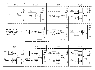
[0019] FIG. 7 and FIG. 8 are diagrams of a signal
processing process for mapping DFT process output samples to
a multicarrier in the clustered SC-FDMA. In particular, FIG.
6 shows an example of applying the clustered SC-FDMA in an
6
CA 02761103 2011-11-04
intra-carrier and FIG. 7 and FIG. 8 shows examples of
applying the clustered SC-FDMA in an inter-carrier.
[0020] Moreover, FIG. 7 shows a case of generating a
signal via a single IFFT block if a subcarrier spacing
between component carriers contiguous to each other is
aligned in a situation that component carriers contiguous to
each other are allocated in a frequency domain. And, FIG. 8
shows a case of generating a signal via a plurality of IFFT
blocks because component carriers are not contiguous to each
other in a situation that component carriers are non-
contiguously allocated in a frequency domain.
[0021] The clustered SC-FDMA may simply extend a DFT
spreading of the conventional SC-FDMA and a frequency
subcarrier mapping configuration of IFFT because a relation
configuration between DFT and IFFT has a one-to-one relation
by applying IFFTs of which number is equal to an arbitrary
number of DFTs. And, the clustered SC-FDMA may be represented
as NxSC-FDMA or NxDFT-s-OFDMA, which may be inclusively named
segmented SC-FDMA according to the present invention.
[0022] FIG. 9 is a diagram of a signal processing process
in the segmented SC-FDMA. Referring to FIG. 9, the segmented
SC-FDMA may be characterized in performing a DFP process by a
group unit in a manner of binding all time-domain modulated
symbols into N groups (N is an integer greater than 1) to
mitigate a single carrier property condition.
7
CA 02761103 2011-11-04
[0023] FIG. 10 is a diagram for describing a signal
processing process for transmitting a reference signal
(hereinafter abbreviated RS) in UL. Referring to FIG. 10,
data is transmitted in a following manner. First of all, a
signal is generated in time domain, transformed by a DFT
precoder, frequency-mapped, and then transmitted via IFFT.
Yet, RS is directly generated in frequency domain by skipping
a step of entering a DFT precoder [S11], enters a localized
mapping step S12, an IFFT step S13 and a CF (cyclic prefix)
attaching step S14 sequentially, and is then transmitted.
[0024] FIG. 11 is a diagram for a structure of a subframe
to transmit RS in case of a normal CP. And, FIG. 12 is a
diagram for a structure of a subframe to transmit RS in case
of an extended CP. Referring to FIG. 11, RS is carried on 4th
OFDM symbol and llth OFDM symbol. Referring to FIG. 12, RS is
carried on 3rd OFDM symbol and 9th OFDM symbol.
[0025] Meanwhile, a processing structure of a UL shared
channel as a transport channel may be described as follows.
FIG. 13 is a block diagram of a process for processing a
transport channel for a UL shared channel. Referring to FIG.
13, after a CRC (cyclic redundancy check) for TB has been
attached to a transport block (hereinafter abbreviated TB)
supposed to be transmitted in UL [130], data information,
which is multiplexed with control information, is divided
into a plurality of code blocks (hereinafter abbreviated CB)
8
CA 02761103 2011-11-04
in accordance with TB size and a CRC for CB is then attached
to each of a plurality of the CBs [131]. Subsequently,
channel coding is performed on a corresponding result value
[132]. Moreover, after a rate matching has been performed on
the channel-coded data [133], the CBs are combined together
[S134]. The combined CBs are then multiplexed with CQI/PMI
(channel quality information/precoding matrix index) [135].
[0026] Meanwhile, the CQI/PMI is channel-coded separately
from the data [136]. The channel-coded CQI/PMI is then
multiplexed with data [135].
[0027] Moreover, RI (rank indication) is channel-coded
separately from the data [137].
[0028] ACK/NACK (acknowledgement/negative acknowledgement)
is channel-coded separately from data, CQI/PMI and RI [138].
And, the multiplexed data and CQI/PMI, the separately
channel-coded RI and the separately channel-coded ACK/NACK
are channel-interleaved to generate an output signal [139].
[0029] In the following description, a physical element
(hereinafter abbreviated RE) for data and control channel in
LTE uplink system may be explained. FIG. 14 is a diagram for
describing a mapping method of physical resources for UL data
and control channel transmission.
[0030] Referring to FIG. 14, CQI/PMI and data are mapped
on RE by a time-first scheme. Encoded ACK/NACK is inserted
around a demodulation reference signal (DM RS) by being
9
CA 02761103 2011-11-04
perforated. RI is rate-matched next to an RE at which
ACK/NACK is situated. Resources for the RI and the ACK/NACK
may occupy maximum 4 SC-FDMA symbols.
[0031]As mentioned in the above description, it may be able
to meet the single carrier property by multiplexing data with
such UL control information (UCI) as CQI/PMI and the like.
Hence, it may be able to accomplish a UL transmission that
maintains a low CM (cubic metric).
[0032]In a system (e.g., LTE Rel-10) resulting from
improving a legacy system, at least one transmission scheme
selected from SC-FDMA and clustered DFTs OFDMA may be
applicable to each component carrier of user equipment for a
UL transmission and may be applicable together with a UL-MIMO
(uplink-MIMO) transmission.
[0033]Meanwhile, regarding the UL transmission structure, a
method of multiplexing data and UCI with each other together
in a UL-MIMO transmission has not been discussed until now.
SUMMARY OF THE INVENTION
[0034]The present invention may provide a method and
apparatus for transmitting data and control information in a
UL MIMO transmission by multiplexing the data and the control
information together.
[0035]Technical tasks obtainable from the present invention
are non-limited the above-mentioned technical task. And,
other unmentioned technical tasks can be clearly understood
from the following description by those having ordinary skill
in the technical field to which the present invention
pertains.
ak 02761103 2014-04-17
[0036]In accordance with one aspect of the invention,
there is provided a method of transmitting an uplink signal
in a wireless communication system. The method is performed
by a user equipment and involves replicating control
information NL times, wherein NL is a number of layers onto
which data transport blocks of a PUSCH (Physical Uplink
Shared Channel) are mapped. The
method further involves
multiplexing the replicated control information in all of
the NL layers of the data transport blocks of the PUSCH,
and transmitting, to a base station, the uplink signal by
using the Ni. layers, the uplink signal including the
replicated control information and the data transport
blocks of the PUSCH.
[0037]The control information may be ACK/NACK
(Acknowledgement/Negative-ACK) information.
[0038]The control information may be RI (Rank
Indication) information.
[0039]The uplink signal may be transmitted via the
PUSCH.
[0040]The Ni layers may include at least one layer.
(004].] The NL may be a number of layers to which the data
transport blocks of the PUSCH may be mapped.
[0042]The control information may have a same rank NL as
the data transport blocks of the PUSCH.
11
ak 02761103 2014-04-17
[0043]In accordance with another aspect of the
invention, there is provided a user equipment for
transmitting an uplink signal in a wireless communication
system. The user equipment includes a transmitting unit
configured to transmit the uplink signal, and a processor
which is configured to replicate control information NL
times, wherein NL is a number of layers onto which data
transport blocks of PUSCH (Physical Uplink Shared Channel)
are mapped. The
processor is further configured to
multiplex the replicated control information in all of the
NL layers of the data transport blocks of the PUSCH, and
transmit, to a base station, the uplink signal by using the
NL layers, the uplink signal including the replicated
control information and the data transport blocks of the
PUSCH.
(0044] The control information may be ACK/NACK
(Acknowledgement/Negative-ACK) information.
[0044a]The control information may be RI (Rank
Indication) information.
[0044b]The uplink signal may be transmitted via the
PUSCH.
[0044c]The NL of layers may include at least one layer.
12
CA 02761103 2014-04-17
[0045]According to the present invention, when data and
control information are transmitted in UL, a rank of the
data
13
CA 02761103 2011-11-04
and a rank of the control information are set equal to each
other. Therefore, signaling overhead may be reduced and
system performance may be raised.
[0046] Effects obtainable from the present invention are
non-limited the above mentioned effect. And, other
unmentioned effects can be clearly understood from the
following description by those having ordinary skill in the
technical field to which the present invention pertains.
DESCRIPTION OF DRAWINGS
[0047] The accompanying drawings, which are included to
provide a further understanding of the invention and are
incorporated in and constitute a part of this application,
illustrate embodiment(s) of the invention and together with
the description serve to explain the principle of the
invention.
[0048] FIG. 1 is a diagram for explaining physical
channels used for 3GPP system and a signal transmission using
the same.
[0049] FIG. 2 is a diagram for describing a signal
processing process for a user equipment to transmit a UL
signal.
[0050] FIG. 3 is a diagram for describing a signal
processing process for a base station to transmit a DL signal.
14
CA 02761103 2011-11-04
[0051] FIG. 4 is a diagram for describing SC-FDAM scheme
for a UL signal transmission and OFDMA scheme for a DL signal
transmission in a mobile communication system.
[0052] FIG. 5 is a diagram for describing a signal mapping
scheme in frequency domain to meet a single carrier property
in the frequency domain.
[0053] FIG. 6 is a diagram of a signal processing process
for mapping DFT process output samples to a single carrier in
the clustered SC-FDMA.
[0054] FIG. 7 and FIG. 8 are diagrams of a signal
processing process for mapping DFT process output samples to
a multicarrier in the clustered SC-FDMA.
[0055] FIG. 9 is a diagram of a signal processing process
in the segmented SC-FDMA.
[0056] FIG. 10 is a diagram for describing a signal
processing process for transmitting a reference signal
(hereinafter abbreviated RS) in UL.
[0057] FIG. 11 is a diagram for a structure of a subframe
to transmit RS in case of a normal CP. And, FIG. 12 is a
diagram for a structure of a subframe to transmit RS in case
of an extended CP.
[0058] FIG. 13 is a block diagram of a process for
processing a transport channel for a UL shared channel.
CA 02761103 2014-04-17
[0059]FIG. 14 is a diagram for describing a mapping
method of physical resources for UL data and control
channel transmission.
[0060]FIG. 15 is a flowchart for a method of efficiently
multiplexing data and control channel together on an uplink
shared channel according to the present invention.
[0061]FIG. 16 is a block diagram for describing a method
of generating a transmission signal of data and control
channel according to the present invention.
[0062]FIG. 17 is a diagram for describing a codeword-to-
layer mapping method.
[0063]FIG. 18 is a block diagram for a configuration of
a device applicable to a base station and a user equipment
to implement the present invention.
DISCLOSURE
[0064]
16
CA 02761103 2011-11-04
[0065] Moreover, in the following description, specific
terminologies are provided to help the understanding of the
present invention. And, the use of the specific terminology
can be modified into another form within the scope of the
technical idea of the present invention.
[0066] In the following description, a method of
efficiently multiplexing data and a control channel on a UL
shared channel by maintaining a single carrier property and
compatibility with a legacy system and an apparatus for the
same according to the present invention are explained.
[0067] FIG. 15 is a flowchart for a method of efficiently
multiplexing data and control channel together on an uplink
shared channel according to the present invention.
[0068] Referring to FIG. 15, a user equipment recognizes a
rank for data of a physical uplink shared channel (PUSCH)
[S150]. Subsequently, the user equipment sets a rank of a UL
control channel (i.e., a control channel may mean such a UL
control information (UCI) as CQI, ACK/NACK, RI and the like)
to the same rank for the data [S151]. And, the user equipment
multiplexes data and control information with each other
[S152]. Thereafter, after the data and the CQI have been
mapped to each other by a time-first scheme, a channel
interleaving may be performed to help the RI to be mapped to
a designated RE and to help the ACK/NACK to be mapped by
perforating RE in the vicinity of DM-RS [S153].
17
CA 02761103 2011-11-04
[0069] Thereafter, the data and the control channel may be
modulated by one of QPSK, 16QAM, 64QAM and the like in
accordance with MCS table [S154]. In doing so, the modulating
step may be shifted to another position (e.g., the modulating
block may be shiftable before the multiplexing step of the
data and the control channel). The channel interleaving may
be performed by a codeword unit or a layer unit.
[0070] As mentioned in the foregoing description, if the
rank of the control channel is restricted to have the same
rank of the data, it may provide several advantages in
viewpoint of signaling overhead. If a data and a control
channel differ from each other in rank, UL DM-RS will be
precoded by the same precoding of the data. Hence, an
additional PMI signaling may be necessary for the control
channel. The same RI for both of the data and the control
channel may simplify the multiplexing chain and may be
helpful to remove an additional signaling. Although there is
one efficient rank for the control channel, a transmitted
rank of the control channel may become the rank of the data.
In viewpoint of a receiving stage, after MIMO decoder has
been applied to each layer, each LLR output may be
accumulated by MRC (maximum ratio combining). In this case,
the LLR (log-likelihood ratio) may mean an output of a
demapper of PSK/QAM and may indicate a value of logarithm
operation of a probability indicating whether a corresponding
18
1
CA 02761103 2011-11-04
bit is set to 0 or 1. For instance, the LLR may be defined as
Formula 1.
[0071] [Formula 1]
LLR(bi,k)= log P[hr,k =114ill
P[br,k = 0r[i]]
[0072] The present invention does not put any limitation
on the multiplexing of data and control channel. In
particular, the above-mentioned same principle may be
applicable to a case of applying TDM (time division
multiplexing) to data and control channel as well.
[0073] The present invention shall be further described in
detail as follows.
[0074] For clarity and convenience of the following
description, assume 2 codewords for data. Yet, the data is
just limited to the 2 codewords for clarity of the following
description, by which the number of the codewords is non-
limited. In particular, the present invention mentioned in he
following description may be identically applicable to at
least two or more codewords. Moreover, the present invention
mentioned in the following description may be independently
applicable per codeword. For example, if a 1st codeword and a
2nd codeword exist, the present invention may be applicable to
the 1st codeword only.
[0075] FIG. 16 is a block diagram for describing a method
of generating a transmission signal of data and control
19
!
CA 02761103 2011-11-04
channel according to the present invention. In FIG. 16, a
position of each block may be changeable in accordance with
an application scheme.
[0076] Assuming two codewords, a channel coding may be
performed on each of the two codewords [160] and a rating
matching may be then performed in accordance with a given MCS
table [161]. Thereafter, encoded bits may be scrambled by a
cell-specific, UE-specific or codeword-specific scheme [162].
[0077] Subsequently, a codeword-to-layer mapping may be
performed [163]. In this process, an operation of layer shift
or permutation may be included.
[0078] FIG. 17 is a diagram for describing a codeword-to-
layer mapping method. The codeword-to-layer mapping may be
performed using the rule shown in FIG. 17. In FIG. 17, a
precoding position may different from the former precoding
position shown in FIG. 13.
[0079] Such control information as CQI, RI and ACK/NACK
may be channel-coded in accordance with a given specification
[165]. In doing so, each of the CQI, RI and ACK/NACK may be
coded using the same channel code for all codewords or may be
coded using a channel code different per codeword.
[0080] Afterwards, the number of encoded bits may be
changed by a bit size control unit [166]. The bit size
control unit may be unified with a channel coding block 165.
A signal outputted from the bit size control unit may be
CA 02761103 2011-11-04
scrambled [167]. In doing so, the scrambling may be performed
cell-specifically, layer-specifically, codeword-specifically
or UE-specifically.
[0081] The bit size control unit may work as follows.
[0082] (1) The control unit recognizes a rank
(n rank pusch) of data for PUSCH.
[0083] (2) A rank (n rank control) of a control channel
is set equal to the rank of the data (i.e., n_rank control =
n rank pusch). The number of bits for the control channel is
extended by being multiplied by the rank of the control
channel.
[0084] One method for performing this may include the step
of copying and repeating a control channel simply. In this
case, the control channel may correspond to an information
level before the channel coding or a bit level coded after
the channel coding. In particular, for instance, in case of a
control channel [a0, al, a2, a3] (i.e., n_bit_ctrl = 4) and
In rank pusch = 2', an extended bit number (next ctrl)
__
includes [a0, al, a2, a3, a0, al, a2, a3] and can become 8
bits.
[0085] In case that the bit size control unit and the
channel coding unit are configured into one, a coded bit may
be generated by applying a channel coding and a rate matching
defined in a legacy system (e.g., LTE Re1-8).
21
I
CA 02761103 2011-11-04
[0086] In addition to the bit size control unit, a bit
level interleaving may be performed to further randomize each
layer. Alternatively, interleaving may be equivalently
performed at a modulated symbol level.
[0087] The CQI/PMI channel and the data for the 2
codewords may be multiplexed by a data/control multiplexer
[164]. While ACK/NACK information in both slots of a subframe
is mapped to RE in the vicinity of UL DM-RS, the channel
interleaver maps the CQI/PMI by a time-first mapping scheme
[168].
[0088] Modulation is performed on each layer [169]. DFT
precoding [170], MIMO precoding [171], RE mapping [172] and
the like are sequentially performed. Thereafter, SC-FDMA
signal is generated and then transmitted via an antenna port
[173].
[0089] Positions of the above function blocks may not be
limited to the positions shown in FIG. 16 and may be
changeable if necessary. For instance, the scrambling blocks
162 and 167 may be positioned next to the channel
interleaving block. And, the codeword-to-layer mapping block
163 may be positioned next to the channel interleaving block
168 or the modulation mapper block 169.
[0090] The method mentioned in the above description may
be performed by a following device. FIG. 18 is a block
diagram for a configuration of a device applicable to a base
22
I
CA 02761103 2011-11-04
station and a user equipment to implement the present
invention. Referring to FIG. 18, a device 100 includes a
processing unit 101, a memory unit 102, an RF (radio
frequency) unit 103, a display unit 104 and a user interface
unit 105. A layer of a physical interface protocol is
performed by the processing unit 101. The processing unit 101
provides a control plane and a user plane. A function of each
layer can be performed by the processing unit 101. The
processing unit 101 may be able to perform the above-
described embodiment of the present invention. In particular,
the processing unit 101 generates a subframe for a user
equipment location determination or may be able to perform a
function of determining a location of a user equipment by
receiving the subframe. The memory unit 102 is electrically
connected to the processing unit 101. And, the memory unit
102 stores operating systems, applications and general files.
If the device 100 is a user equipment, the display unit 104
may be able to display various kinds of informations. And,
the display unit 104 may be implemented using a well-known
device such as an LCD (liquid crystal display), an OLED
(organic light emitting diode) display and the like. The user
interface unit 105 may be configured by being combined with
such a well-known user interface as a keypad, a touchscreen
and the like. The RF unit 103 is electrically connected to
23
1
CA 02761103 2011-11-04
the processing unit 101. The RF unit 103 transmits or
receives a radio signal.
[0091] According to the present invention mentioned in the
above description, as mentioned in the foregoing description,
data and control information are processed in case of a UL
transmission. Therefore, signaling overhead may be reduced
and system performance may be enhanced.
[0092] The aforementioned embodiments are achieved by
combination of structural elements and features of the
present invention in a predetermined type. Each of the
structural elements or features should be considered
selectively unless specified separately. Each of the
structural elements or features may be carried out without
being combined with other structural elements or features.
Also, some structural elements and/or features may be
combined with one another to constitute the embodiments of
the present invention. The order of operations described in
the embodiments of the present invention may be changed. Some
structural elements or features of one embodiment may be
included in another embodiment, or may be substituted with
corresponding structural elements or features of another
embodiment. Moreover, it will be apparent that some claims
referring to specific claims may be combined with another
claims referring to the other claims other than the specific
24
I
I
CA 02761103 2011-11-04
claims to constitute the embodiment or add new claims by
means of amendment after filing the application.
[0093] According to the present invention, a user
equipment (UE) may be replaced by such a terminology as a
mobile station (MS), a subscriber station (SS), a mobile
subscriber station (MSS), a mobile terminal and the like.
[0094] Moreover, a user equipment of the present invention
may include one of PDA (Personal Digital Assistant), cellular
phone, PCS (Personal Communication Service) phone, GSM
(Global System for Mobile) phone, WCDMA (Wideband CDMA) phone,
MBS (Mobile Broadband System) phone and the like.
[0095] Embodiments of the present invention can be
implemented using various means. For instance, embodiments of
the present invention can be implemented using hardware,
firmware, software and/or any combinations thereof.
[0096] In case
of the implementation by hardware, a method
according to each embodiment of the present invention can be
implemented by at least one selected from the group
consisting of ASICs (application specific integrated
circuits), DSPs (digital signal processors), DSPDs (digital
signal processing devices), PLDs (programmable logic devices),
FPGAs (field programmable gate arrays), processor, controller,
microcontroller, microprocessor and the like.
[0097] In case of the implementation by firmware or
software, a method according to each embodiment of the
I
ak 02761103 2014-04-17
present invention can be implemented by modules, procedures,
and/or functions for performing the above-explained functions
or operations. Software code is stored in a memory unit and
is then drivable by a processor. The memory unit is provided
within or outside the processor to exchange data with the
processor through the various well-known means.
[0098] While the present invention has been described and
illustrated herein with reference to the preferred
embodiments thereof, it will be apparent to those skilled in
the art that various modifications and variations can be made
therein without departing from the scope of the invention.
Thus, it is intended that the present invention covers the
modifications and variations of this invention that come
within the scope of the appended claims and their
equivalents. And, it is apparently understandable that an
embodiment is configured by combining claims failing to have
relation of explicit citation in the appended claims together
or can be included as new claims by amendment after filing an
application.
INDUSTRIAL APPLICABILITY
[0099] Accordingly, the present invention is applicable to
a user equipment, a base station and other equipments in a
wireless mobile communication system.
26