Note : Les descriptions sont présentées dans la langue officielle dans laquelle elles ont été soumises.
CA 02762505 2011-12-20
COMMUNICATIONS DEVICE INCLUDING RADIO FREQUENCY (RF) SIGNAL
BLOCKING LAYER FOR NEAR-FIELD COMMUNICATION (NFC) DEVICE
AND RELATED METHODS
Technical Field
[0001] This application relates to the field of
communications, and more particularly, to communications devices
and related methods that use near-field communication (NFC).
Background
[0002] Mobile communication systems continue to grow in
popularity and have become an integral part of both personal and
business communications. Various mobile devices now incorporate
Personal Digital Assistant (PDA) features such as calendars,
address books, task lists, calculators, memo and writing
programs, media players, games, etc. These multi-function
devices usually allow electronic mail (email) messages to be
sent and received wirelessly, as well as access the Internet via
a cellular network and/or a wireless local area network (WLAN),
for example.
[0003] Some mobile devices incorporate contactless card
technology and/or near-field communication (NFC) chips. NFC
technology is used for contactless short-range communications
1
CA 02762505 2011-12-20
based on radio frequency identification (RFID) standards, using
magnetic field induction to enable communication between
electronic devices, including mobile wireless communications
devices. These short-range communications include payment and
ticketing, electronic keys, identification, device set-up
service and similar information sharing. This short-range high
frequency wireless communications technology exchanges data
between devices over a short distance, such as only a few
centimeters. NFC circuitry may also be implemented in other
communications devices, such as NFC tags, for example.
Brief Description of the Drawings
[0004] FIG. 1 is a schematic block diagram of a
communications device in accordance with an example embodiment
including a near-field communication (NFC) circuit device and a
radio frequency (RF) signal blocking layer to block RF signal
communication by the NFC circuit device.
[0005] FIG. 2 is a schematic block diagram of the
communications device of FIG. 1 with the RF signal blocking
layer removed to permit RF signal communication by the NFC
circuit device.
[0006] FIG. 3 is a perspective view of an example embodiment
of the communications device of FIG. 1 including a frangible
scratch-off RF signal blocking layer.
[0007] FIG. 4 is a perspective view of an example embodiment
of the communications device of FIG. 1 including an adhesive
peel-off RF signal blocking layer.
[0008] FIG. 5 is a schematic block diagram of a
communications device in accordance with an alternative example
embodiment including an RF signal blocking dielectric layer
configured to block RF signal communication between NFC
circuitry and an associated antenna.
2
CA 02762505 2011-12-20
[0009] FIG. 6 is a schematic block diagram of the
communications device of FIG. 5 with the RF signal blocking
dielectric layer removed.
[0010] FIG. 7 is a schematic block diagram of a
communications device in accordance with another alternative
example embodiment including a power blocking dielectric layer
configured to block powering of NFC circuitry by a battery.
[0011] FIG. 8 is a schematic block diagram of the
communications device of FIG. 7 with the power blocking
dielectric layer removed.
[0012] FIG. 9 is a schematic block diagram illustrating
example components which may used in the communications devices
of FIGS. 1 through 8.
Detailed Description
[0013] The present description is made with reference to the
accompanying drawings, in which example embodiments are shown.
However, many different embodiments may be used, and thus the
description should not be construed as limited to the
embodiments set forth herein. Rather, these embodiments are
provided so that this disclosure will be thorough and complete.
Like numbers refer to like elements throughout, and prime
notation is used to indicate similar elements or steps in
alternative embodiments.
[0014] Generally speaking, a communications device is
disclosed herein which may include a near-field communication
(NFC) circuit device, and a radio frequency (RF) signal blocking
layer adhesively coupled with the NFC circuit device. The RF
signal blocking layer may be configured to block RF signal
communication by the NFC circuit device while coupled therewith.
As such, the RF signal blocking layer may advantageously be used
to prevent communication with the NFC circuit device prior to
3
CA 02762505 2011-12-20
purchasing the communications device at a store, etc., for
enhanced security and privacy.
[0015] More particularly, the RF signal blocking layer may
comprise an electrical conductor. In accordance with an example
embodiment, the RF signal blocking layer may comprise a
frangible layer. In another example embodiment, a pressure-
sensitive adhesive layer may be included for adhesively securing
the RF signal blocking layer to the NFC circuit device.
[0016] The NFC circuit device may include a package and NFC
circuitry may be carried by the package, and the communications
device may further include a wireless communications circuit
carried by the package. By way of example, the NFC circuit
device may comprise active NFC circuitry or passive NFC
circuitry, and an antenna coupled thereto.
[0017] A similar communications device may include a NFC
circuit device, an antenna coupled to the NFC circuit device,
and an RF signal blocking dielectric layer removably positioned
between the NFC circuit device and the antenna. The RF signal
blocking dielectric layer may be configured to block RF signal
communication between the NFC circuit device and the antenna
when positioned therebetween, and upon removal permit RF signal
communication between the NFC circuit device and the antenna.
[0018] Yet another similar communications device may include
a battery, an NFC circuit device, and a power blocking
dielectric layer removably positioned between the battery and
the NFC circuit device. The power blocking dielectric layer may
be configured to block powering of the NFC circuit device by the
battery when positioned therebetween, and upon removal permit
powering of the NFC circuit device by the battery.
[0019] A related method aspect is for making a communications
device and may include adhesively coupling an RF signal blocking
layer with a NFC circuit device. The RF signal blocking layer
4
CA 02762505 2011-12-20
may be configured to block RF signal communication by the NFC
circuit device while coupled therewith.
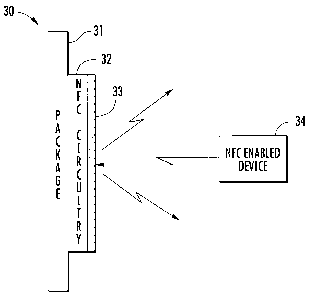
[0020] Referring initially to FIGS. 1 and 2, a communications
device 30 illustratively includes a near-field communication
(NFC) device including NFC circuitry 32 and a package 31
carrying the NFC circuitry 32. In the illustrated example, the
package 31 comprises a substrate (e.g., plastic, dielectric,
etc.) and the NFC circuitry 32 is shown carried on an exterior
surface of the package 31, but in some embodiments the NFC
circuitry 32 may be embedded or encased within the package 31,
for example. The communications device 30 further illustratively
includes a radio frequency (RF) signal blocking layer 33
adhesively coupled with the NFC circuit device. In particular,
in this embodiment the RF signal blocking layer 33 is adhesively
coupled to the NFC circuitry 32, but in some embodiments it may
be coupled to the package 31, such as when the NFC circuitry 32
is embedded within the package 31, for example.
[0021] The RF signal blocking layer 33 is advantageously
configured to block RF signal communication by the NFC circuitry
32 while coupled therewith (or to the package 31 in some
embodiments). As shown in FIG. 1, this prevents an NFC enabled
device 34 from communicating with the NFC circuitry 32, but NFC
communication is enabled or permitted upon removal of the RF
signal blocking layer 33 (FIG. 2). In some embodiments, the
communications device 30 may further include one or more
wireless communications circuits carried by the package 31, such
as those of the communications subsystem 1001 described further
below with reference to FIG. 9. The package 31 may take
different forms in different embodiments, such as a card
substrate, circuit board, portable device housing, etc.
[0022] By way of background, NFC is a short-range wireless
communications technology in which NFC-enabled devices are
CA 02762505 2011-12-20
"swiped," "bumped" or otherwise moved in close proximity to
communicate. In one non-limiting example implementation, NFC may
operate at 13.56 MHz and with an effective range of about 10cm,
but other suitable versions of near-field communication which
may have different operating frequencies, effective ranges,
etc., for example, may also be used.
[0023] The use of the RF signal blocking layer 33 for the NFC
circuitry 32 may be advantageous in various applications.
Because of the relatively small dimensions in which NFC circuits
or tags may be implemented, it is possible to use them in
numerous product identification and security applications. For
example, in retail sales applications, NFC tags may be embedded
in coupons, gift cards, collectible cards or figures, etc. The
information stored in the NFC tag may be associated with
rebates, purchase points, or an account credit (e.g., a monetary
credit, a digital media content or application download credit,
etc.,), for example. Thus, a designated user or recipient may
use an NFC enabled device 34 to access the information, which
may provide greater ease of use and convenience.
[0024] Nonetheless, because of the value of the information
stored by such NFC tags, some may attempt to surreptitiously
access these NFC tags to steal the information. The RF signal
blocking layer 33 advantageously prevents the NFC circuitry 32,
which may be implemented either as passive NFC circuitry or
active NFC circuitry in various embodiments, from communicating
until the RF signal blocking layer 33 is removed. Using an
example where the communications device 30 is a gift card for
loading credits onto a mobile device (e.g., mobile device
application or "app" credits), the RF signal blocking layer 33
would advantageously prevent scanning of the gift card by
someone other than the intended recipient. Moreover, if the RF
signal blocking layer 33 was removed, then it would be visually
6
CA 02762505 2011-12-20
evident that the card had been tampered with by someone other
than the intended recipient.
[0025] By way of example, the RF signal blocking layer 33 may
comprise an electrical conductor. Referring more particularly to
FIG. 3, in this example embodiment the RF signal blocking layer
33' is frangible, meaning that it separates, breaks, or
otherwise comes off in pieces or sections. More particularly,
the RF signal blocking layer 33' comprises a "scratch-off"
layer, similar to those found on lottery tickets or game cards,
but with conductive (e.g., metal) particulates therein that
advantageously block RF signals. The RF signal blocking layer
33' may therefore easily be removed by scratching or rubbing
with a coin 35', etc.
[0026] Another example is shown in FIG. 4, in which a
pressure sensitive adhesive layer 36" may be included for
adhesively securing the RF signal blocking layer 33" to the
package 31" so that it may be peeled off of the package. In
this example, the package 31" comprises a portable electronic
device housing, and the pressure sensitive adhesive layer 36"
and RF signal blocking layer 33" peel off as a single unitary
body or piece (i.e., as a whole). However, in some embodiments
perforations, etc., may be used so that the pressure sensitive
adhesive layer 36" and RF signal blocking layer 33"
combination is frangible, i.e., it comes apart when peeled off
so that it may not be replaced in its original form. Considered
alternatively, this destroys the RF signal blocking layer 33"
Another approach is that the pressure sensitive adhesive layer
36" may comprise a single-use adhesive, which may not provide
for easy reapplication of the RF signal blocking layer 33" once
removed. Again, this may be used to help ensure that evidence of
tampering cannot easily be hidden by reapplication of the RF
signal blocking layer 33".
7
CA 02762505 2011-12-20
[0027] Another example embodiment of a communications device
50 is shown in FIG. 5. Here, NFC circuitry 52 (passive NFC
circuitry in the illustrated example) is carried by a package
51, and an antenna 57 is also carried by the package 51. An
electrical connector 58, such as a spring or bias clip, is used
to electrically couple or connect the NFC circuitry 52 with the
antenna 57. An RF signal blocking dielectric layer 53 is
removably positioned or removably coupled to disrupt electrical
contact between the NFC circuitry 52 and the antenna 57 at the
electrical connector 58. The RF signal blocking dielectric layer
53 may comprise a dielectric strip or sheet of material that
interrupts signal flow between the NFC circuitry 52 and the
antenna 57 when positioned or coupled therebetween. As such, the
RF signal blocking dielectric layer 53 similarly blocks (i.e.,
by preventing, limiting, obstructing, etc.) operation of the NFC
circuitry 52 as does the RF signal blocking layer 33 described
above, but through blocking of RF signals downstream of the
antenna 57 instead of upstream (i.e., blocking the signals from
reaching the antenna in the first place). Upon removal of the RF
signal blocking dielectric layer 53 (FIG. 6), the electrical
connector 58 then provides an electrical connection between the
NFC circuitry 52 and the antenna 57 so that NFC communication
may take place.
[0028] Referring additionally to FIGS. 7 and 8, yet another
example implementation of the communications device 50' may
include a battery 59' carried by the package 51', and a power
blocking dielectric layer 53' removably coupled or positioned
between the battery and the NFC circuitry 52'. In this case, the
NFC circuitry 52' comprises active NFC circuitry, and coupling
or positioning of the power blocking dielectric layer 53'
between the NFC circuitry and the battery 59' at the electric
connector 58' advantageously prevents powering of the NFC
8
CA 02762505 2011-12-20
circuitry. Upon removal of the power blocking dielectric layer
53' (FIG. 8), powering of the NFC circuitry 52' by the battery
59' may occur.
[0029] Example components of a communications device 1000
that may further be used in accordance with the above-described
embodiments are now described with reference to FIG. 9. The
device 1000 illustratively includes a housing 1200, a keypad or
keyboard 1400 and an output device 1600. The output device shown
is a display 1600, which may comprise a full graphic LCD. Other
types of output devices may alternatively be utilized. A
processing device 1800 is contained within the housing 1200 and
is coupled between the keyboard 1400 and the display 1600. The
processing device 1800 controls the operation of the display
1600, as well as the overall operation of the mobile device
1000, in response to actuation of keys on the keyboard 1400.
[0030] The housing 1200 may be elongated vertically, or may
take on other sizes and shapes (including clamshell housing
structures). The keyboard may include a mode selection key, or
other hardware or software for switching between text entry and
telephony entry.
[0031] In addition to the processing device 1800, other parts
of the mobile device 1000 are shown schematically in FIG. 9.
These include a communications subsystem 1001; a short-range
communications subsystem 1020; the keyboard 1400 and the display
1600, along with other input/output devices 1060, 1080, 1100 and
1120; as well as memory devices 1160, 1180 and various other
device subsystems 1201. The mobile device 1000 may comprise a
two-way RF communications device having data and, optionally,
voice communications capabilities. In addition, the mobile
device 1000 may have the capability to communicate with other
computer systems via the Internet.
9
CA 02762505 2011-12-20
[0032] Operating system software executed by the processing
device 1800 is stored in a persistent store, such as the flash
memory 1160, but may be stored in other types of memory devices,
such as a read only memory (ROM) or similar storage element. In
addition, system software, specific device applications, or
parts thereof, may be temporarily loaded into a volatile store,
such as the random access memory (RAM) 1180. Communications
signals received by the mobile device may also be stored in the
RAM 1180.
[0033] The processing device 1800, in addition to its
operating system functions, enables execution of software
applications 1300A-1300N on the device 1000. A predetermined set
of applications that control basic device operations, such as
data and voice communications 1300A and 1300B, may be installed
on the device 1000 during manufacture. In addition, a personal
information manager (PIM) application may be installed during
manufacture. The PIM may be capable of organizing and managing
data items, such as e-mail, calendar events, voice mails,
appointments, and task items. The PIM application may also be
capable of sending and receiving data items via a wireless
network 1401. The PIM data items may be seamlessly integrated,
synchronized and updated via the wireless network 1401 with
corresponding data items stored or associated with a host
computer system.
[0034] Communication functions, including data and voice
communications, are performed through the communications
subsystem 1001, and possibly through the short-range
communications subsystem. The communications subsystem 1001
includes a receiver 1500, a transmitter 1520, and one or more
antennas 1540 and 1560. In addition, the communications
subsystem 1001 also includes a processing module, such as a
digital signal processor (DSP) 1580, and local oscillators (LOs)
CA 02762505 2011-12-20
1601. The specific design and implementation of the
communications subsystem 1001 is dependent upon the
communications network in which the mobile device 1000 is
intended to operate. For example, a mobile device 1000 may
include a communications subsystem 1001 designed to operate with
the MobitexTM, Data TACTM or General Packet Radio Service (GPRS)
mobile data communications networks, and also designed to
operate with any of a variety of voice communications networks,
such as AMPS, TDMA, CDMA, WCDMA, PCS, GSM, EDGE, etc. Other
types of data and voice networks, both separate and integrated,
may also be utilized with the mobile device 1000. The mobile
device 1000 may also be compliant with other communications
standards such as 3GSM, 3GPP, UMTS, 4G, etc.
[0035] Network access requirements vary depending upon the
type of communication system. For example, in the Mobitex and
DataTAC networks, mobile devices are registered on the network
using a unique personal identification number or PIN associated
with each device. In GPRS networks, however, network access is
associated with a subscriber or user of a device. A GPRS device
therefore typically involves use of a subscriber identity
module, commonly referred to as a SIM card, in order to operate
on a GPRS network.
[0036] When required network registration or activation
procedures have been completed, the mobile device 1000 may send
and receive communications signals over the communication
network 1401. Signals received from the communications network
1401 by the antenna 1540 are routed to the receiver 1500, which
provides for signal amplification, frequency down conversion,
filtering, channel selection, etc., and may also provide analog
to digital conversion. Analog-to-digital conversion of the
received signal allows the DSP 1580 to perform more complex
communications functions, such as demodulation and decoding. In
11
CA 02762505 2011-12-20
a similar manner, signals to be transmitted to the network 1401
are processed (e.g. modulated and encoded) by the DSP 1580 and
are then provided to the transmitter 1520 for digital to analog
conversion, frequency up conversion, filtering, amplification
and transmission to the communication network 1401 (or networks)
via the antenna 1560.
[0037] In addition to processing communications signals, the
DSP 1580 provides for control of the receiver 1500 and the
transmitter 1520. For example, gains applied to communications
signals in the receiver 1500 and transmitter 1520 may be
adaptively controlled through automatic gain control algorithms
implemented in the DSP 1580.
[0038] In a data communications mode, a received signal, such
as a text message or web page download, is processed by the
communications subsystem 1001 and is input to the processing
device 1800. The received signal is then further processed by
the processing device 1800 for an output to the display 1600, or
alternatively to some other auxiliary I/O device 1060. A device
may also be used to compose data items, such as e-mail messages,
using the keyboard 1400 and/or some other auxiliary I/O device
1060, such as a touchpad, a rocker switch, a thumb-wheel, or
some other type of input device. The composed data items may
then be transmitted over the communications network 1401 via the
communications subsystem 1001.
[0039] In a voice communications mode, overall operation of
the device is substantially similar to the data communications
mode, except that received signals are output to a speaker 1100,
and signals for transmission are generated by a microphone 1120.
Alternative voice or audio I/O subsystems, such as a voice
message recording subsystem, may also be implemented on the
device 1000. In addition, the display 1600 may also be utilized
in voice communications mode, for example to display the
12
CA 02762505 2011-12-20
identity of a calling party, the duration of a voice call, or
other voice call related information.
[0040] The short-range communications subsystem enables
communication between the mobile device 1000 and other proximate
systems or devices, which need not necessarily be similar
devices. For example, the short-range communications subsystem
1020 may include an infrared device and associated circuits and
components, NFC or a BluetoothTM communications module to provide
for communication with similarly-enabled systems and devices.
[0041] Many modifications and other embodiments will come to
the mind of one skilled in the art having the benefit of the
teachings presented in the foregoing descriptions and the
associated drawings. Therefore, it is understood that various
modifications and embodiments are intended to be included within
the scope of the appended claims.
13