Note : Les descriptions sont présentées dans la langue officielle dans laquelle elles ont été soumises.
CA 02763807 2011-11-28
WO 2011/002637 PCT/US2010/039544
MU_IJTI ELEMENT CONTACT ASSEMBLIES FOR ELECTRICAL
STIMULATION SYSTEMS AND SYSTEMS AND METHODS OF MAKING AND
USING
FIELD
The present invention is directed to the area of implantable electrical
stimulation systems and methods of making and using the systems. The present
invention is also directed to implantable electrical stimulation leads (and
lead
extensions) having multi-element contact assemblies, as well as methods of
inalcing
and using the leads (and lead extensions), rulii-element contact assemblies,
and
electrical stimulation systems.
B AC:KGROU N.( )
l.mplartable electrical stimulation systems have proven therapeutic in a
variety
of diseases and disorders. For example, spinal cord stimulation systems have
been
used as a therapeutic modality for the treaty-nernt of chronic pain syndromes.
Peripheral nerve stimulation has been used to treat chronic pain syndrome and
incontinence, with a number of other applications under investigation.
Functional
electrical stimulation systems have been applied to restore some functionality
to
paralyzed extremities in spinal cord injury patients.
Stimulators have been developed to provide therapy for a variety of
treatments. A stimulator can include a control module (with a pulse
generator), one or
more leads, and an array of stimulator electrodes on each lead. The stipulator
electrodes are in contact with or near the nerves, muscles, or other tissue to
be
stimulated. The pulse generator in the control module generates electrical
pulses that
are delivered by the electrodes to body tissue.
Conventional implanted electrical stimulation systems are often incompatible
with magnetic resonance imaging (" MRT") due to the large radio frequency
("RE")
pulses used daring MRL The RE pulses can generate transient signals in the
conductors and electrodes of an implanted lead. These signals can have
deleterious
effects including, for example, unwanted heating of the tissue causing tissue
damage,
induced currents in the lead, or premature failure of electronic components.
CA 02763807 2011-11-28
WO 2011/002637 PCT/US2010/039544
BRIEF SUMMARY"
In one embodiments, an implantable lead includes a lead body having a distal
end, a proximal end., and a longitudinal length. A plurality of electrodes are
disposed
on the distal end of the lead body.. plurality of terminals are disposed on
the
proximal end of the lead body. A plurality of conductors are disposed in the
lead
body such that each conductor electrically couples at least one of the
electrodes to at
least one of the terminals. At least one of the electrodes or at least one of
the
terminals includes a multi-element contact assernbly. The multi-elerne.nt
contact
assembly includes at least one conductive inner element and at least one
conductive
outer element disposed over the inner clement. At least one of the plurality
of
conductors is electrically coupled to one of the multi--element contact
assemblies such
that the conductor is positioned against the at least one inner eler ent. The
at least
one outer element includes a region that is in contact with the at. least one
inner
element.
in another embodiment, a method for forming an implantable lead includes
disposing a plurality of elongated conductors in a lead body of the lead such
that ends
of the conductors extend from ends of the lead body. A multi-element contact
assembly is disposed at one of the onus of the lead body. The multi-element
contact
assembly includes an inner element and an outer element disposed over the
inner
element. An end of one of the plurality of conductors is disposed into the
rnulti.
clement contact assembly such that the conductor is positioned against the at
least one
inner element. A region of the at least one outer element is contacted with
the at least
one inner element.
In yet another embodiment, a method for forming an implantable lead includes
disposing a plurality of elongated conductors in a lead body of the lead such
that ends
of the conductors extend from ends of the lead body. Each of the ends of the
conductors extending from one end of the lead body are physically attached to
one of
a different one of a plurality of inner elements. A different one of a
plurality of outer
elements are disposed individually over each of the inner elements to form a
plurality
of multi-element contact assemblies. Each of the multi-clement contact
assemblies
-2-
CA 02763807 2011-11-28
WO 2011/002637 PCT/US2010/039544
includes a one of the outer elements disposed around a one of the inner
elements.
Each of the inner elements of the multi-element contact assemblies are
contacted to
the corresponding outer elements.
BRIEF DESCRIPTION OF THE DRAWINGS
Non-limiting and non-exhaustive embodiments of the present invention are
described with reference to the following drawings. In the dravAngs, like
reference
numerals refer to like parts throughout the various figures unless otherwise
specified.
For a better understanding of the present invent i on, -reference will be made
to
Iii the following Detailed Description, which is to be read in association
with the
accompanying drawings, wherein.
FIG. 1 is a schematic view of one embodiment of an electrical stimulation
system, according to the invention;
FIG. 2 is a schematic view of another embodiment of an electrical stimulation
system, according to the invention,
FIG. 3A is a schematic view of one embodiment of a proximal portion of a
lead and a control module of an electrical stimulation system, according to
the
invention;
FIG. 3B is a schematic view of one embodiment of a proximal portion of a
lead and a leadextersion of an electrical stimulation system, according to the
invention;
FIG. 4 is a schematic side view of one embodiment of portions of a plurality
of conductors disposed along a conductor placement sleeve, the conductors
configured into units, according to the invention.;
FIG. S is a schematic longitudinal cross-sectional view of one embodiment of
portions of a plurality of conductors disposed in an elongated member,
according to
the invention;
FIG. 6A is a schematic side view of one embodiment of a plurality, of portions
of conductors formed into two units that include alternating single-coil
regions and
multi-coil regions, according to the invention;
FIG; 6B is a schematic longitudinal cross-sectional view of one embodiment
of the portions of conductors of FIG. 6A, according to the invention;
CA 02763807 2011-11-28
WO 2011/002637 PCT/US2010/039544
1<IG, 7A is a schematic end view of one embodiment of a conductor-carrying
element of an electrical stimulation system, according to the invention;
FIG. 713 is a schematic end view of one embodiment of conductors disposed in
the conductor-carrying element of FIG. 7A, according to the invention;
FIG. 8A is a schematic end view of one embodiment of a rn lli-element
contact assembly disposed at one end of the conductor-carrying element of FIG.
7A,
one ofthe conductors of the conductor-carrying element positioned for coupling
electrically with the multi-element contact assembly, according to the
invention;
FIG. 8B is a schematic side view of one embodiment of the multi -cleinerit
contact assembly of FIG. 8A disposed at one end of the conductor-carrying
clement of
FIG. 'A, according to the invention;
FIG, 8C is a schematic side view of one embodiment of a second multi-
element contact assembly disposed at one end of the conductor-carrying element
of
FIG. 7A, according to the invention;
FIG, 9.:!\. is a schematic end view of one embodiment of a mull-element
contact assembly disposed at one end of a conductor-carrying element, one of
the
conductors of the co.rductor-carrying element positioned for coupling
electrically with
the multi-element contact assembly, according to the invention;
FIG, 913 is a, schematic side view of one err-r-rodiment of the multi-element
contact assembly of FIG. 9A disposed at one end of the conductor-carrying
element of
FIG. 9A, according to the invention; and
FIG. 1.0 is a schematic overview of one embodiment of components of a
stimulation system., including an electronicsubassembly disposed within a
control.
module, according to the invention.
DETAI LED DESCRIPTION
The present invention is directed to the area of implantable electrical
stimulation systems and methods of making and using the systems; The present
invention is also directed to implantable electrical stimulation leads (and
lead
extensions) having multi-element contact assemblies, as well as methods
ofmaking
and using the leads (arid lead externsions), multi-element contact assemblies,
and
electrical stimulation systems.
-4-
CA 02763807 2011-11-28
WO 2011/002637 PCT/US2010/039544
Suitable implantable electrical stimulation systems include, but are not
limited
to, an electrode lead ("lead") with one or more electrodes disposed on a
distal end of
the lead and one or more terminals disposed on one or more proximal ends of
the
lead. Leads include, for example, percutaneous leads, paddle leads, and cult
leads,
Examples of electrical stimulation systems with leads are found in, for
exa~rmple, U.S.
Patents Nos. 6;181,969 6,516,227; 6,609,029; 6,609,032; and 6,741,892; and U.
Patent Applications Serial Nos. 10/353,101, 10/503,281, 11/238,240:
11/319,291;
11./327,880; 1 l/375,638; 11/393,991; and 11/396,309, all of which are
incorporated
by reference.
Figure 1 illustrates schematically one embodiment of an electrical stimulation
system 100. The electrical stimulation system includes a control module (e,
g., a
stimulator or pulse generator) 102, a paddle body 104, and at least one lead
body. 106
coupling the control module 102 to the paddle body 104. :l'fie paddle body 1
04 and
the one or more lead bodies 106 form a lead, The paddle body 104 typically
includes
an array of electrodes 134. The control module 102 typically includes an
electronic
subassembly 1.10 and an optional power source 120 disposed in a sealed housing
114.
The control nodule 102 typically includes a connector 144 (Figure 2 and 3A,
see also
32.. and 350 of-F' 3B) into which the proximal end of the one or more lead
bodies
106 can be plugged to make an electrical connection via conductive contacts on
the
control module 102 and terminals (e.g., 310 i_n :l gure 3A and 336 of Figure
3B) on
each of the one or more lead bodies 106. It will be understood that the
electrical
stimulation system can include more, fewer, or different components and can.
have a
variety of different configurations including those configurations disclosed
in the
electrical stimulation system references cited herein.. For example, instead
of a paddle
body 104, the electrodes 134 can be disposed in an array at or near the distal
end of
the lead body 106 forming a percutaneous lead, as illustrated in Figure 2. A
percutarreous lead may be isodiametric along the length of the lead, In
addition, one
or more lead extensions 312 (see Figure 3 B) can be disposed between the one
or more
lead bodies 106 and the control module 102 to extend the distance between the
one of
more lead bodies 106 and the control module 102 o'Lthe embodiments shown in
Figures 1 and 2.
CA 02763807 2011-11-28
WO 2011/002637 PCT/US2010/039544
The electrical stimulation system or components of the electrical stimulation
system, including one or more of the lead bodies 106, the paddle body 104, and
the
control module 102, are typically implanted into the, body of a patent. The
electrical
stimulation syste n can be used for a variety of applications including, but
not limited
to, brain stimulation, neural stimulation, spinal cord stimulation, muscle
stimulation,
and the like.
The electrodes 134 can be formed Using any conductive, biocompatible
material. Examples of suitable materials include metals, alloys, conductive
polymers,
conductive carbon, and the like, as well as combinations thereof. The number-
of
electrodes 134 in the array of electrodes 134 may vary. For exarrrple, there
can be
two, four, six, eight, ten, twelve, fourteens sixteen, or more electrodes 134.
As will be
recognized, other numbers of electrodes 134 may, also be used.
The electrodes of the paddle body 104 or one or more lead bodies 106 are
typically disposed in, or separated by, a non-conductive, iocompatible
material
including, for example, silicone, polyurethane, polyetheretth:erketone (.`PE
FK"),
epoxy, and the like or combinations thereof. The paddle body 104 and one or
more
lead bodies 106 may be formed in the desired shape by any process including,
for
example, molding (including injection molding), casting, and the like.
Electrodes and
connecting wires can be disposed onto or within a paddle body either prior to
or
subsequent to a molding or casting process. The non-conductive material
typically
extends from the distal end of the lead to the proximal end of each of the one
or more
lead bodies 106. The non-conductive, b ocompauble material of the paddle body
104
and the one or more lead bodies 106 may be the same or different. The paddle
body
104 and the one or more lead bodies 106 may be a unitary structure or can be
formed
as two separate structures that are permanently or detachably coupled
together.
Terry inals (e.g., 310 in Figure 3A and 336 of Figure 3B) are typically
disposed
at the proximal end of they one or more lead bodies 106 for connection to
corresponding conductive contacts (e. ,T., 314 in figure 3A and 340 of-Figure
313) in
connectors (e.g., 144 in Figures l-3A and 322 and 350 of Figure 313) disposed
on, for
example, the control module 1.02 (or to other devices, such as conductive
contacts or,
a lead extension, an operating room cable, or an adaptor). Conductive wires
("conductors") (not shown) extend from the terrninais (e.g,, 310 in Figure 31
and 336
-6-
CA 02763807 2011-11-28
WO 2011/002637 PCT/US2010/039544
of Figure 3B) to the electrodes 134. Typically, one or more electrodes 134 are
electrically coupled to a terminal (e.g,, 310 in Figure 3A and 336 of Figure
313), In
some embodiments, each t :rr lrn l (, g., 310 in Figure 3A and 336 of Figure
313) is
only connected to one electrode 134, The conductive wires may be embedded in
the
Anon-conductive material of the lead or can be disposed in one or more lumens
(not
shown) extending along the lead. In some embodiments, there is an individual
1111-nen
for each conductive wire. In other embodiments, two or more conductive wires
may,
extend through a lumen. "There may also .he one or snore lumens (not shown)
that
open at, or near, the proximal end of the lead, for example, for inserting a
stylct rod to
1.0 -facilitate placement of the lead within a body of a patient.
Additionally, there may
also be one or more lumens (not shown) that open at, or near, the distal end
of the
lead, for example, for infusion of drugs or medication into the site of iron
plantation of
the paddle body 104, In at least one embodiment, the one or more lumens may be
flushed continually, or on a regular basis, with saline, epidural fluid, or
the like. In at
least some embodiments, the one or more lumens can be permanently or removably
sealable at the distal end,
In at least some embodiments, leads are coupled to connectors disposed on
control modules. In Figure 3A, a lead 308 is shown configured and arranged 'or
insertion to the control module 102. The connector 144 includes a connector
housing
302. The connector housing 302 defines at least one port 304 into which a
proximal
end 306 of a lead 308 with terminals 3 10 can be inserted, as shown by
directional
arrow 312. The connector housing 302 also includes a plurality of conductive
contacts 314 for each port 304. When the lead 308 is inserted into the port
304, the
conductive contacts 314 can be aligned w rith the terminals 3 10 on the lead
308 to
electrically couple the control module 102 to the electrodes (134 of Figure 1)
disposed
at a distal end of the lead 308, Examples of connectors in control modules are
found
in, for example, tl.S. Patent No. 7,244,150 and U.S. Patent Application Serial
No.
1 l /532,844, which are incorporated by reference.
In Figure 3B, a connector 322 is disposed on a lead extension 324. The
connector 322 is showni disposed at a distal end 326 of the lead extension
324. The
connector 322 includes a connector housing 328. The connector housing 328
defines
at least one port 330 into which a proximal end 332 of a lead 334 with
terminals 336
CA 02763807 2011-11-28
WO 2011/002637 PCT/US2010/039544
can be inserted, as shown by directional arrow 338. The connector housing 328
also
includes a plurality of conductive contacts 340. When the lead. 334 is
inserted into the
port 330, the conductive contacts 340 disposed in the connector :housin 328
can be
aligned with the terminals 336 on the lead 3 34 to electrically couple the
lead
extension 324 to the electrodes (134 of Figure 1) disposed. at a distal end
(not shown)
of the lead 334.
In at least some embodiments, the proximal end of a lead extension is
similarfly configured and arranged as a proximal end of a lead. The lead
extension
324 may include a plurality of conductive wires (not shown) that electrically
couple
the conductive contacts 340 to a proximal end 348 of the lead extension 324
that is
opposite to the distal end 326. In at least some embodiments, the conductive
wires
disposed in the lead extension 324 can be electrically coupled to a plurality
of
terminals (not shown) disposed on the proximal end 348 of the lead extension
324. In
at least some embodiments, the proximal end 348 of the lead extension X24 is
configured and arranged for insertion into a connector disposed in anther lead
extension. In other embodiments, the proximal end 348 of the lead extension
324 is
con- figured and arranged for insertion into a connector disposed in a control
module.
As an example, in Figure 313 the proximal end 348 of the lead extension 324
.is
inserted into a connector 350 disposed in a control module 352.
One or more of the conductors connecting at least one terminal to an electrode
(or other conductive contact) can be arranged in a conductor path to eliminate
o
reduce the effect of l~ l- irradiation, such as that generated during magnetic
resonance
imaging ( MR1 "). The conductor path includes a plurality of limits arranged
in series.
in some embodiments, the units are disposed along a single continuous
conductor. In
other embodiments, the units are separate conductive elements electrically
coupled
together.
Each unit includes at least three conductor segments that at least partially
overlap one another to form a multi-coil region. First, each unit includes a
first
conductor segment that extends in a first direction. along a longitudinal
length of an
elongated member (e.g.; a lead or bead. extension) from a beginning point to a
first
position. Second, each unit includes a second conductor segment that extends
from
the first position hack towards (and possibly past) the beginning point to a
second
- t -
CA 02763807 2011-11-28
WO 2011/002637 PCT/US2010/039544
position. Third, each w -fit includes a third conductor segment that extends
in the first
direction from. the second position to an endpoint. in at least some
enibodi.rnents, the
first position is between the second position and the endpoint; In at least
some
embodiments, the second position is between the beginning point and the first
position. In at least some embodiments, the unit may include a single-coil
region
flanking at least one end of themulti-coil region.
The units may be electrically continuous such that the endpoint of a first
unit
is the beginning point of the next consecutive unit. At least one of the
beginning
points may be .a terminal or an electrode (or other conductive contact).
Likewise, at
least one of the endpoints may be a terminal or an electrode (or other
conductive
contact), In preferred embodiments, the conductor segments are each coiled. In
at
least some embodiments, the conductor segments are coiled around a conductor
placement sleeve. In at least some en}bodiments, the conductor placement
sleeve
defines a lumen that optionally is configured and arranged to receive a
stiffening
member (e.g., a stylet, or the like).
In at least some embodiments, at least one of the first, second, or third
conductor segments is substantially straight. In at least some embodiments,
the first
and third conductor segments are substantially straight and the second
conductor
segment is coiled. In at least some other embodiments, all three conductor
segments
are substantially straight. It will be understood that, the term
"substantially straight
conductor segment" means that the conductor segment is not coiled. A
"'substantially
straight conductor segment" may be carried, particularly when the lead itself
is curved
(see, for example, Figure 1).
In at least some embodiments, the conductor segments are all formed from the
same length of conductive material (e.g., wire or the like). The conductors
may have
a single filament or be multi-fd.ar. In preferred embodiments, the conductors
are
multi-filar. In at least some embodiments, two or more of the conductor
segments can
be individual pieces of conductive material that are electrically coupled.
(e.g., soldered
or welded) together. In at least some embodiments, a layer of insulation
("conductor
insulation") is disposed over each of the conductor segments.
CA 02763807 2011-11-28
WO 2011/002637 PCT/US2010/039544
In at least some embodiments, the length of conductor used in the second
conductor segment is at least 1.5, 1.75, 1.9, 2, 2.1, 2.25, or 2-5 times the
length of
either the first conductor segment or the third conductor segment. It will be
recognized, however, that this ratio of conductor-segment lengths may vary
among
embodiments, particularly if the thickness of the conductor or thickness of
the layer of
conductor insulation is different for the different segments.
Figure 4 schematically illustrates one embodiment of a plurality of conductors
402. The conductors 402 are configured into a plurality of units, such as unit
404.
Each unit includes a first conductor segment 404a, a second conductor segment
404b,
and a third conductor segment 404c. In at least some embodiments, conductor
insulation is disposed over the conductors 402 to electrically isolate each of
the
conductors 402 from one another.
Many different numbers of units may be disposed along longitudinal lengths
of the conductors 402 including, for example, two, three, four., five, six,
seven, eight,
nine, tent, twelve, fifteen, twenty, twe-rnty-fve, thirty, forty, fifty, or
more .Units, It Will
be understood that many other numbers of units may be employed as well. When a
plurality of units are coupled together in series along a longitudin al length
of one or
more conductors, the plurality of units form a repeat.ng series of single-coil
regions,
such as the single-coil regions 406, separated from one another by a multi-
coil region,
such as the multi-coil region 408.
In at least some embodiments, the conductors 402 are disposed along a.
conductor placement sleeve 410. The conductor placement sleeve 410 can be
formed
from any suitable biocompatible material including, for example, one or more
polymers. In at least some embodiments, conductor insulation is disposed over
the
conductors 402 to encapsulate the conductors 402 and electrically isolate the
conductors 402 from one another.
In at least some embodiments, one or more conductors having one or more
units may be disposed in an elongated member (e. g. a lead or lead extension).
in at
least some enmbodiments, the ends of the conductors 402 can be coupled to
terminals,
electrodes, or conductive contacts. In preferred emnnbodiuments, each of the
conductors
in an elongated met-fiber are configured into units. In at least some
embodiments, only
-10-
CA 02763807 2011-11-28
WO 2011/002637 PCT/US2010/039544
a subset of the conductors disposed in an elongated member include one or more
units, the remaining conductors having a different arrangement (tor example, a
single
conductor segment between the ternmrinal(s) and elec.trode(s)/conductive
contact(s)).
Conductors, such as the conductors 402, may be disposed in a lurnen of an
elongated member (e.g., a lead, lead extension, or the like). Figure 5 is a
schematic
longitudinal cross-sectional view of one embodiment of portions of a plurality
of
conductors 502 disposed in an. elongated member 504. The illustrated portions
of the
conductors 502 includes unit 506, shown between two vertical dotted lines.
Unit 506
includes a first conductor segment 506a, a second conductor segment 706b, and
a
third conductor segment 506c. In at least some embodiments, the conductors 502
are
disposed over a conductor placement sleeve 508. In at least some embodiments,
the
conductor placement sleeve 508 defines a lumen 510. The elongated member 504
includes a body 512 and a lumen 514 into which the conductors 502 are
disposed.
Figure 6A schematically illustrates a side view of one embodiment of a
1.5 plurality of conductors 602 each includin ; units 604 and 606. In Figure
6A, the first
second, and third conductor segments 604a, 604b (not shown in Figure 6A), and
6040,
respectively, of the unit 604, and the f irst, second, and third conductor
segments 606a,
6061 (not shown in Figure 6A), and 606c, respectively, of the unit 606, are
each
coiled. The conductors 602 are arranged such that the conductors include multi-
coil
regions 608 and single-coil regions 610, In at least some embodiments, the
conductors 602 may be coiled around one or more objects, such as a conductor
placement sleeve 612.
Figure 6B is a schematic longitudinal cross-sectional view of the plurality of
conductors 602 disposed in an outer layer 614 of a body 615 of a lead 616.
When the
outer layer 614 of the body 615 is isodiametric along the longitudinal length
of the
lead 616, open spaces 6181 may form between the single-coil regions, such as
single-
coil region 606a, and the outer layer 614.
Typically, one or more contacts (e.g., terminals, electrodes, connective
contacts, or the like) are disposed at opposing ends of an elongated member
(e.g., a
lead, a lead extension, or the like).. The contacts disposed. on opposite ends
oft the
elongated member~ are electrically coupled together by elongated conductors
CA 02763807 2011-11-28
WO 2011/002637 PCT/US2010/039544
extending along a longitudinal length of the elongated member. For example,
terminals disposed on a. proximal end of the conductor may be coupled, via
conductors, to electrodes (or connective contacts) disposed can a distal end
of the
elongated member. During formation of the elongated member, the conductors may
be disposed along a body of the elongated zneÃt-iber in any number of
different
arrangements including, for example, configured into one or more units (as
described
above with reference to Figures 4-611), wrapped around a sleeve or mandrel,
extending substantially straight, disposed in one or more conductor-carrying
elements,,
or the like).
It is desirable that the connections between the conductors and the contacts
be
strong enough to maintain a viable electrical connection during implantation
and
throughout the operational life of the electrical stimulation system within a
patient, A
loss of electrical connection between a conductor and a contact may result in:
a loss of
therapeutic stimulation and may even necessitate an undesired explantation of
the
electrical stimulation system from the patient.
The connection between the conductor and the contact is sometimes made by a
heat-related method of coupling (e.g., laser welding, resistance welding,
brazing,
soldering, or the like). A heat-related method of coupling alone, however, may
not
provide sufficient strength to maintain an electrical connection between the
conductor
and the contact throughout the operational life of the electrical stimulation
system.
In some cases the conductor may also be mechanically clamped to the contact.
Heat produced by the heat-related nethod of coupling, however, typically
anneal:, the
contact in a region of the contact in immediate proximity to the site of the
heat-related
coupling. The annealing may reduce the tensile strength of the conductor, One
known attempt to separate the mechanical clamping from the heat-related
coupling
involved crimping sleeves to the ends of conductors, and then coupling the
sleeves to
the contacts. Uaforttanately, manufacturing and handling sleeves that are
small
enough for clamping to the ends of conductors is tedious and complex.
In at least some embodiments, multi-element contact assemblies (''`contact
assemblies") are e ployed to electrically couple with contacts. The contact
assemblies include a rigid (or semi-rigid), cylindrically-shaped outer element
and a
-12-
CA 02763807 2011-11-28
WO 2011/002637 PCT/US2010/039544
rigid (or semi-rigid) inner element that is disposed in the outer element. In.
at least
some embodiments, the inner element is disposed concentrically in the outer
element,
The contacts electrically couple to the contact assemblies by positioning the
conductors against the inner elements and contacting the outer elements and
the inner
elements. In at least sonic embodiments, the outer elements are mechanically
deformed to electrically couple the conductors to at least one of the inner
elements or
the outer elements. In at least some embodiments, the conductors are also
electrically
coupled to the contact assemblies by physically attaching the conductors to
the
contact assemblies. in at least some embodiments, the conductors are
physically
attached to the contact assemblies by one or more heat-related coupling
methods.
In at. least some embodiments, both inner elements and outer elements are
formed from conductive materials. In at least some embodiments, a contact
assembly
is positioned at an end ofa. body of an elongated member and one of the
conductors is
positioned in the contact asserribly such that the conductor is either
internal or
external to the inner element. in at least some embodiments, the outer element
is
mechanically deformed (e.g, bent, crimped, swaged, Molded, creased, or the
like) to
press against one or more of the conductor and the inner clement, thereby
electrically
coupling the conductor to at least one of the inner element or the outer
element. In at
least some embodiments, the conductor is also physically attached to one or
more of
the inner element or the outer element by a heat-related method of coupling
(e.g.,
laser welding, resistance welding; brazing. soldering, or the like), either
before or
after the outer element is mechanically deformed. In at least some
enibodirnents, the
outer element and the inner element are physically attached together (e.g, by
a heat-
related coupling method) after the outer element is mechanically deformed.
As discussed above, conductors may be disposed along the body ofthe
elongated member in any number of different arrangements including, for ex
arrrple,
configured into one or more units, wrapped around a sleeve or mandrel,
extending
substantially straight, disposed in one or more conductor:-carrying elements,
or the
like. It will be understood that, when one or .more conductors are coiled
(e.g.,
configured into one or more units, or the like), the coils may extend to the
electrodes,
terminals, or both.
-13-
CA 02763807 2011-11-28
WO 2011/002637 PCT/US2010/039544
In at least some embodiments, a conductor-carrying element may be used to
retain one or more conductors along at least a portion. of an. elongated
member.
Figure 71< . is a schematic end view of one embodiment of a conductor-carrying
element 702 that includes multiple lurnens. The conductor-carrying element 702
defines a central lumen 704 and conductor lumens 706-713.. The conductor-
carrying
element 702may include many different configurations and many different
numbers
and sizes of conductor lumens.
In at least some embodiments, one or more conductors extend along at least a
portion of a longitudinal length of the lead body within one of the conductor
lumens
706-713. In at least some embodiments, ends of the conductors extend from an
end of
the conductor-carrying element 702. Figure 7B is a schematic end view of one
embodiment of the conductors 720-727 disposed in the conductor-carrying
clement
702. Ina( least some embodiments, insulation 730 is disposed around a
longitudnal
length of one or more of the conductors 720-727. Ends of the conductors 720-
727
extend from the end of the conductor-carrying element 702. The extending ends
of
the conductors 720-727 on one end of the conductor-carrying element 702 are
typically coupled to terminals mid the extending ends of the conductors 720-
727 on
the other end of the conductor-carrying element 702 are typically coupled to
electrodes (or connector contacts).
A contact assembly may be disposed at one end of the conductor-carrying
element 702 which, ,in turn, may be disposed in a lead body or a lead
extension body.
The end of one of the conductors 720-727 extending from the conductor-carrying
element 702 may be coupled to the conductor assembly. figures 7B-913 show
conductors extending along lumens defined in conductor-carrying elements.
In some embodiments, the conductor-carrying element 702 extends the entire
lengt of a lead body (or a lead extension body). In other embodiments, one or
more
conductor-carrying elements extend along potions of the length of a lead body
(or a
lead extension body). in at least some embodiments, a lead body (or a lead
extension
body) also includes one or more outer layers disposed over the one or a xore
conductor-carrying tiler eats. In at least some embodiments, contact
assemblies are
coupled with conductors that extend along lead bodies (or lead extension
bodies) that
do not include conductor-carrying elements,
-14-
CA 02763807 2011-11-28
WO 2011/002637 PCT/US2010/039544
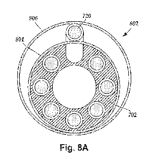
Figures 8A and 8B are schematic end and side views, respectively., of one
embodiment of a first contact assembly 802 disposed at one end of the
conductor-
carrying element 702. The first contact assembly 802 includes an inner
element. 804
and an outer element 806. In at least some embodiments, the outer element 806
functions as a contact (e.g., a terminal, an electrode, or the like).
In preferred embodiments, the lead is isodiametric. Accordingly, in at least
some embodiments, the outer element 806 has a diameter that is equal to a
diameter of
a lead body or a lead extension body). In at least some embodiments, the inner
element 804 has a diameter that is equal to the diameter of the conductor-
carrying
element 702.
The inner element 804 and the outer element 806 can be formed using any
rigid or semi-rigid, conductive, biocompatible material, ,xamples of suitable
materials include platinum, iridium, platinum iridium, titanium, alloys of any
of the
above-listed metals, super alloys (e.g., MP35N and the like), stainless steel,
and the
Iike, as well as combinations thereof. It will be understood that the inner
element 804
and the outer element 806 may be formed from either the same material or
different
materials.
In at least some embodiments, the inner element 804 is disposed within the
outer element 806 such that the inner element 804 and the outer element 806
are
concentric to one another. In at least some embodiments, the outer element 806
is
cylindrical. In at least some embodiments, the inner element 804 is also
cylindrical.
In at least some embodiments, the inner element 804 is C-shaped. In at least
some
embodiments, the outer element 806 is C-shaped,
In at least some embodiments, the first contact assembly 802 is disposed at
one end of the conductor-carrying element 702. In at least some embodiments,
one of
the conductors 720-727 extending from the end of the conductor-carrying
element
702 is coupled to the first contact assembly 802 and the re aining conductors
720-
727 are extended through the inner element 804.. In at least sonic
embodiments, the
remaining conductor 720-727 that extend through the first contact assembly 802
are
coupled to one or more additional contacts subsequently positioned laterally
from the
- 15.
CA 02763807 2011-11-28
WO 2011/002637 PCT/US2010/039544
first contact assembly 802. In Figure 8B and in other figures, only a few
conductors
are shown to represent the conductors 721-727, for clarity of illustration.
In Figures 8A and 8B, conductor 720 is shown coupled to the first contact
assembly 802. The conductor 720 is positioned against the inner element 804
such
that the conductor 720 is disposed external to the inner element 804 and
internal to the
outer element 806. Once the conductor 720 is disposed external to the inner
element
804 and internal to the outer element 806, the outer element 806 is deformed
(e.g.,
mechanically deformed) to press the conductor 720 against at least one of the
inner
clement 804 or the outer element 806 thereby electrically coirpl nzg the
conductor 720
to at least one of the inner element 804 or the outer element 806. in at least
some
embodimentsõ the outer element 806 is mechanically deformed (e.g., bent,
crimped,
swaged, folded, creased, or the like). In at least some embodiment, the
conductor 720
is positioned against the inner element 804 such that the conductor 720 is
disposed
internal to the inner element 804.
In. at least some embodiments, the conductor 720 is also electrically coupled
to
one or more of the inner element 804 or the outer element 806 by, physically
attaching
the conductor 720 to one or more of the inner element 804 or the outer element
806,
In at least some embodiments, the conductor 720 is physically attached to one
or more
of the inner element 804 or the outer element 806 by a heat-related method of
attachment (e.g., laser welding, resistance welding, brazing, soldering, or
the like).
The conductor 720 may beelectrically coupled, via the heat-related method of
coupling, to one or more of the inner element 804 or the outer element 806
either
before or after the conductor 720 is electrically coupled to one or more of
the inner
element 804 or the outer element 806 by mechanical deformation of the outer
element
806, In at least some embodiments, the inner element 804 and the outer element
806
are coupled together, via, the heat-related method of coup: Brag, after the
conductor 720
is electrically coupled to one or more of the inner element 804 or the outer
element
806 by mechanical deformation of the outer element 806.
As discussed above, insulation 730 may be disposed over the lot gibadinal
length of one or more of the conductors 720-727. In at least some embodiments,
the
insulation 730 of the conductor 720 is removed over at least a portion of the
region of
the conductor 720 coupled to the first contact assembly 802 prior to
mechanical
-16-
CA 02763807 2011-11-28
WO 2011/002637 PCT/US2010/039544
deformation of the outer element 806. In other embodiments, the mechanical
deformation process removes enough of the insulation 730 to provide adequate
electrical connection between the conductor 720 and at least one of the inner
element
804 or the outer element 806 without needing to remove a. portion of the
insulation
730 prior to performing the mechanical deformation process.
In. at least some embodiments, once a first end of the first contact assembly
802 is positioned against the conductor-carrying element 702 and an electrical
connection is made between the conductor 720 and the first contact assembly
802; a
spacer 808 may be positioned adjacent to a second end of the first contact
assembly
802 opposite to the first end. The conductors 721-727 extending through the
inner
element 804 of the contact assembly 802 also extend through the spacer 808. In
at
least some embodiments, when a tip (not shown) of the conductor 720 extends
beyond
the second end of the first contact assembly 802, the tip of the conductor 720
may be
rezoned or bent so that the tip of the conductor 720 does not obstruct the
spacer 808
from abutting the First contact assembly 802.
An additional contact assembly may be positioned at the opposite end of the
spacer from the first contact assembly and another conductor mays be coupled
to the
additional contact assembly. It will be understood that any number of contact
assemblies r nay be coupled to conductors and separated from one another by
spacers.
In. at least some embodiments, the number of contact assemblies is equal to
the
number of conductors. It will further be understood that the same process may
be
repeated on an opposing end of the conductor-carrying element 702.
Figure 8C'. is a schematic side view of one embodiment of a second contact
assembly 820 disposed it one end of the conductor-carrying clement 702. The
conductor 721 is positioned between, and electrically coupled to, an inner
element
822 and an outer element 824 of the second contact assembly 820. The remaining
conductors 722-727 extend through the inner element 822. The spacer 808
separates
the first contact assembly 802 from. the second contact assembly 820.
In at least some embodiments, the outer elements 806 and 824 both function as
terminals or both function as electrodes. In preferred embodiments, if one or
more
additional contact assemblies are disposed on the same end of the conductor-
carrying
17-
CA 02763807 2011-11-28
WO 2011/002637 PCT/US2010/039544
element 702 and separated from one another by spacers, the outer element(s) of
those
additional contact assemblies also function as outer elements 806 and 824. In
at least
some embodiments, one or more contact assemblies disposed on the opposite end
of
the, conductor-carrying element 702 each have carter elements that function as
the
other of either terminals or electrodes, depending on the functionality of the
outer
elements 806 and 824.
In an alternate ernbodirnent, a conductor is physically attached Lo a C-shaped
inner element via a heat-related method of coupling. An outer element is then
disposed over the inner element (and the electrically coupled conductor), and
at least a
portion of the outer element and the inner element are physically attached
together. In
at least some embodiments, the inner element is substantially flat when the
conductor
is physically attached to the inner elernea t. In which case, the inner
element is bent
into a "C" shape after the physical attachment of the conductor toy the inner
element.
In some embodiments, the conductor is electrically coupled to an inner surface
of the
l inner element. In other embodiments, the conductor is electrically coupled
to an outer
surface of the inner element.
Figure 9A is a schematic end vie of one embodiment of a cor tact assembly
902 disposed at one end of a conductor-carrying element 904. The contact
assembly
902 includes a C--shaped inner element 906 and a cylindrical outer element
908.
conductors, such as conductor 910, are disposed in. the condr.rcÃor-carrying
element
904. Figure 9B is a schematic side view of one embodiment of the contact
assembly
902 disposed at one end of the conductor-carrying element 904 and the
conductor 910
coupled to the inner element 906 hich., in turn, is coupled to the outer
element 908.
In preferred embodiments, the diameter of the outer element 908 is equal to
the
diameter of a lead body (or lead extension body) in which the conductor-
carrying
element 904 is disposed.
In Figures 9A and 9B, the conductor 910 is shown electrically coupled to an
inner surface 912 of the inner element 906. It will be understood that the
conductor
910 may, instead, be electrically coupled to an outer surface of the inner
element 906.
In at least some embodiments, the outer element 908 is disposed over the inner
element 906 such that the inner element 906 is compressed within the outer
element
908.
-ts-
CA 02763807 2011-11-28
WO 2011/002637 PCT/US2010/039544
Once the outer element 908 is disposed over the inner element 906, the outer
element 908 is electrically coupled to the inner element 906. In some
embodiments,
the outer element 908 is mechanically deformed to press against the inner
element
906. In other embodiments, the outer element is physically attached to the
inner
element. 906 by a heat-related method of coupling (e.., laser welding,
resistance
welding, braying, soldering, or the like). In at least some embodiments, the
outer
element 908 and the inner element 906 are electrically coupled by both
mechanical
deformation of the outer element 908 and physical attachment.
In at least some embodiments, each of the conductors of the conductor-
carrying element 904 are physically attached to a different inner element. The
inner
elements are arranged along an axis of the end of the conductor-carrying
element 904
such that the conductors coupled to the more lateral inner elements extend
through
each of the more medial inner elements. Outer elements are positioned over,
and
electrically coupled to, each inner element_ In at least some embodiments, at
least one
of the elements may be closed to t-orma continuous transverse path.
In at least some embodiments, the inner element 906 has a longitudinal length
914 (shown in Figure 9B as a two-headed arrow) that is not equal to a
longitudinal
length 916 (also shown in Figure 9B as a two-headed arrow) of the outer
element 908.
In at least some embodiments, the longitudinal length 916 of the outer element
908 is
?0 greater than the longitudinal length 91.4 of the inner element 906. It mays
bean
advantage to have the outer clement 908 of the contact assembly 902 being
greater in
length than the inner element 906 so that.. when the conductor 910 is coupled
to the
inner element 906, but not yet coupled to the outer element 908, the axial
positioning
of the inner element 906 may be adjusted without needing to axially adjust the
outer
element 908. Thus, the outer element 908 may be positioned as desired without
needing to axially adjust the outer element 908 to accommodate the positioning
of the
electrical coupling of the outer element 908 with the conductor 910.
Figure 10 is a schematic overview of one embodiment of components of
electrical stimulation system 1000 including an electronic subassembly 1010
disposed
within a control module. It will be understood that the electrical stimulation
system
can include more, fewer, or different components and can have a variety of
different
39
CA 02763807 2011-11-28
WO 2011/002637 PCT/US2010/039544
configurations including those configurations disclosed in the stimulator
references
cited herein.
Some of the components (for example, power source 1012, antenna 1018,
receiver 1002, and processor 1004) of the electrical stimulation system can be
positioned on one or more circuit hoards or similar carriers within a sealed
housing of
an implantable pulse generator, if desired. Any power source 1012 can he used
including, for example, a battery such. as a primary battery or a rechargeable
battery.
Examples of other power sources include super capacitors, nuclear or atomic
batteries, mechanical resonators, infrared collectors, thermally-powered
energy
sources, flexural powered energy sources, bioenergy power sources, fuel cells,
hioelectric cells, osmotic pressure pumps, and the like including the power
sources
described in U.S. Patent Application l"ublicatiot? No, 2004/0059392,
incorporated
herein by reference.
As another alternative, power can be supplied by an external power source
through inductive coupling via the optional antenna 1.018 or a secondary
antenna.
The external power source can be in a device that is mounted on the skin of
the user
or in a unit that is provided near the user on a permanent or periodic basis,
if the power source 1012 is a rechargeable battery, the battery may be
recharged using the optional antenna 1.018, if desired. Power can he provided
to the
battery for recharging by inductively coupling the battery through the antenna
to a
recharging unit 1016 external to the user. Examples of such arrangements can
he
found in the references identified above.
In one embodiment, electrical current is emitted by the electrodes 134 on the
paddle or lead body to stimulate none fibers, muscle fibers, or other body
tissues near
the electrical stimulation system. A processor 1004 is generally included to
control
the timing and electrical characteristics of the electrical stimulation
system. For
example, the processor 1004 can, if desired, control one or more of the
timing,
frequency, strength, duration.. and waveform of the pulses. In addition, the
processor
1004 can select which electrodes can be used to provide stimulation, if
desired. In
some embodiments, the processor 1004 may select which electrode(s) are
cathodes
and which electrode(s) are anodes. In some embodirtments, the processor 1004
may be
CA 02763807 2011-11-28
WO 2011/002637 PCT/US2010/039544
used to identify ~uhi.ch electrodes provide the most useful stimulation of the
desired
tissue.
Any processor can be used and can be as simple as an electronic device that,
for example, produces pulses at a regular interval or the processor can be
capable of
receiving and interpreting instructions from an external programming unit 1008
that,
for example, allows modification of pulse characteristics . In the illustrated
embodiment, the processor 1004 is coupled to a receiver 1002 which, in turn.
is
coupled to the optional antenna 1018. This allows the processor 1004 to
receive
instructions from an external source to, for example, direct the pulse
characteristics
and the selection of electrodes, if desired.
In one embodiment, the antenna 1018 is capable of receiving signals (e.g,, RF
signals) from an external telemetry unit 1006 ,which is programmed by a
programming unit 1008. The programming unit 1008 can be external to, or part
of,
the telemetry unit 1006, The telemetry unit 1006 can be a device that is warn
on the
skin of the user or can be carried by the user and can have a form similar to
a. pager,
cellular phone, or remote control, if desired. As another alternative, the
telemetry unit
1006 may not be worn or carried by the user but may only be available at a
home
station or it a clinician's office. The programming unit 1008 can be any unit
that can
provide information to the telemetry unit 1006 for transmission to the
electrical
stimulation system 1000. The programming unit 1008 can be part of the
telemetry
unit 1006 or can provide signals or informatioi to the telemetry unit 1006 via
a
wireless or sired connection. One example of a suitable programming unit is a
computer operated by the user or clinician to send signals to the telemetry
unit 1006.
The signals sent to the processor 1004 via the antenna 1.018 and receiver 1002
can be used to modify or otherwise direct the operation of the electrical
stimulation
system. For example, the signals may be used to modify the pulses of the
electrical
stimulation system such as modifying one or more of pulse duration, pulse
srequency,
pulse waveform, and. pulse strength. The signals may also direct the
electrical
stimulation system 1000 to cease operation, to start operation, to start
charging the
battery, or to stop charging the battery. In other embodiments, the
stimulation system
does not include an antenna 1018 or receiver 1002 and the processor 1004
operates as
proararn.m ed.
-21-
CA 02763807 2011-11-28
WO 2011/002637 PCT/US2010/039544
Optionally, the electrical stimulation system 1000 may include a transmitter
(tort shown) coupled to the processor 1004 and the antenna 1018 for
transmitting
signals bade to the telemetry Ernie 1006 or another unit capable of receiving
the
signals. For example, the electrical stimulation system 1000 mays transmit
signals
indicating whether the electrical stimulation system 1000 is operating
properly or not
or Indicating when the battery needs to be charged or the level of charge
remaining in
the battery. The processor 1004 may also be capable of transmitting
information
about the pulse characteristics so that a user or clinician can determine or
verify the
characteristics.
The above specification, examples and data provide a description of the
manufacture and use of the composition of the invention. Since many
embodiments
of the invention can be made without departing from the spirit and scope of
the
invention, the invention also resides in the claims hereinafter appended.