Note : Les descriptions sont présentées dans la langue officielle dans laquelle elles ont été soumises.
CA 02763850 2011-11-29
WO 2010/142946 PCT/GB2010/001116
I
AN ELECTRICALLY SMALL ULTRA-WIDEBAND ANTENNA FOR MOBILE
HANDSETS AND COMPUTER NETWORKS
Technical Field of the Invention
This invention relates to an antenna arrangement and particularly to an
electrically small
antenna operable across a wide range of frequencies and more particularly to
an
electrically small antenna suitable for use in instantaneous ultra-wideband
applications.
Background to the Invention
Ultra-wideband (UWB) is a wireless radio technology which allows the user to
transmit
large amounts of data across a very wide range of frequencies. Ultra-wide band
systems
have applications in many fields such as high-speed, short range, wireless
communication; computer networks; radar and geolocation systems; imaging; and
medical systems.
In recent years there has been significant interest in the development of
electrically
small, but efficient antennas capable of operating across a wide bandwidth or
at multiple
frequencies, where electrically small is generally considered to mean that an
antenna
has no dimension larger than X./10. The ability to monitor the electromagnetic
spectrum
with a single, electrically small and portable antenna would be highly
desirable.
Therefore, there is a requirement for an antenna having the following
electrical and
physical characteristics; compact, lightweight, robust, low cost and an ultra-
wideband
frequency response covering at least the frequency range 20 MHz - 6 GHz. This
bandwidth would allow coverage of traditional HF and UHF bands while extending
operation to the higher frequency Wireless Local Area Network (WLAN) and
future
3G/4G (3-5 GHz) spectrums. However, achieving an electrically small antenna
that is
reasonably radiation efficient and operates over such a wide bandwidth is
challenging
and various solutions which claim to optimise different combinations of
properties have
been proposed. In the past, full coverage has only been achieved by clustering
a
number of different antennas such as combinations of wire, disk cone and bow-
tie
CA 02763850 2011-11-29
WO 2010/142946 PCT/GB2010/001116
2
antennas; however this requires costly and bulky feed networks. Alternatively,
several
monopoles of varying heights above a ground plane have been used. However this
solution does not provide an instantaneous UWB capability but instead the
monopoles
work in a stepped time sequence when transmitting and receiving data.
Particular applications such as detection and measurement systems require omni
directional radiation patterns. For these applications, in particular, one
option is to
focus on monopole and dipole antennas and the present invention is a
development of
the monopole antenna.
It is known that the impedance bandwidth performance of a traditional monopole
antenna can be improved by top loading with an additional capacitive sleeve.
McLean et
al (McLean, J., Foltz, H., and Crook, G. "Broadband, Robust Low-profile
Monopole
Incorporating Top Loading, Dielectric Loading, and a Distributed Capacitive
Feed
Mechanism", IEEE International Symposium on Antennas and Propagation, July,
pp.
1962-1965, 1999) proposed the directly connected wire stem feed of a
conventional top
loaded monopole, with a capacitive sleeve. The proposed aperture coupled wire
stem
feed to the top loaded monopole exploits the attendant frequency variation in
reactance
slope, which improves the impedance matching bandwidth. The capacitive sleeve
further increases the capacitive effect of the top loaded structure, therefore
decreasing
the Q factor, which increases bandwidth but with lossy effects. Further
enhancement of
the matching bandwidth is desirable without the lossy effects.
CA 02763850 2011-11-29
WO 2010/142946 PCT/GB2010/001116
3
Summary of the Invention
It is an object of the present invention to provide an electrically small
antenna
arrangement with improved impedance matching bandwidth and reduced lossy
effects.
Accordingly the present invention provides an antenna arrangement for use in
an UWB
network, the antenna arrangement comprising a ground plane, a coaxial feed and
an
antenna element, wherein the antenna element comprises:
a cylindrical conductive case isolated from the ground plane by a first
dielectric
material;
a second dielectric material contained within the cylindrical conductive case;
a conductive core extending from the coaxial feed through the first dielectric
material
and into the second dielectric material; and
a top loaded structure electrically connected to the cylindrical conductive
case and
electrically insulated from the conductive core,
the antenna element being configured as a shorted coaxial section.
The adoption of a coaxial to coaxial aperture connection permits increased
matching
bandwidth with reduced lossy effect. The term "coaxial" is used to mean a
shielded
electrical cable constructed with precise conductor dimensions and spacing in
order to
function efficiently as a radio frequency transmission line. The coaxial is
capable of
propagating a transverse electromagnetic wave (TEM), allowing a RF bandwidth
in
principle of up to 18GHz to be propagated along the cable. Any abrupt change
in the
relative dimensions causes increased reflection, reducing the quality of the
transmitted
power. For this reason it is preferred that the core of the coaxial feed is
extended
beyond the ground plane to act as the core of the antenna element without need
for a
change in dimension or a connection of any sort. Top loading the antenna
element
increases the capacitance effect of the antenna so that the physical structure
may be
reduced in height. This allows the core of the antenna to act as a monopole
feed at less
than a quarter wave length in height but does not have the detrimental effect
of
generating out of phase reflections normally associated with reducing the
height below
that of a/4.
CA 02763850 2011-11-29
WO 2010/142946 PCT/GB2010/001116
4
In the simplest form of antenna construction the first and second dielectric
material used
can be air. Surrounding the core of the antenna element with dielectric
material
increases the vertical current moment and improves radiation efficiency,
decreasing
feed point reactance and feed point voltage which decreases the Q factor
resulting in
increased bandwidth capability. The dielectric value of a material depends on
its
permittivity. The choice of material used relates to its higher or lower
capacitive effect.
Air has a dielectric value of l which is less than PTFE
(polytetrafluoroethylene) with a
dielectric value of 2 because PTFE has higher permittivity. Increasing the
permittivity
of the second dielectric material enhances the performance of the antenna
arrangement.
One particular embodiment of the invention uses air as the first dielectric
material and
PTFE as the second. A person skilled in the art will appreciate that other
combinations
of dielectric materials can be used. Furthermore, encasing the antenna element
in a
third dielectric material can offer further reductions in the Q factor and
therefore gains
in bandwidth. Also the use of a solid dielectric provides structural support
and will
enhance robustness.
The top loaded structure can be varied in its shape and construction and can
be made
from any metallic material. The simplest form is a shorting end cap
electrically
connected to a cylindrical conductive case (which is comprised from a section
of the
outer case of a semi rigid coaxial). However, other forms such as wires,
spirals and
plates etc can be used. The preferred embodiment uses an enlarged "top hat"
disc
structure. The disc can also be sub divided into a number of discrete
sections, like a
Goubau top loaded antenna (IEEE Transactions on Antennas and Propagation Vol.
AP-
30, No. 1, January 1982), with spacing between each section to further improve
the
capacitance of the antenna arrangement and hence reduce the physical height of
the
antenna further.
Ensuring there is a gap between the cylindrical conductive case and the ground
plane
and using air for the first dielectric material allows the increase of the
capacitance effect
of the antenna arrangement and therefore the bandwidth capability but with
reduced
lossy effects. Also by adjusting the gaps between the top loaded structure and
the end of
CA 02763850 2011-11-29
WO 2010/142946 PCT/GB2010/001116
the conductive core GI and also between the cylindrical conductive case and
the ground
plane G2 can allow the antenna arrangement to be fine tuned to ensure the
ideal
impedance matching bandwidth is obtained.
The antenna arrangement can further include a plurality of radial fins which
act as
spatial polarisation filters. The fins may comprise fast or slow surface wave
structures
that. act as High Impedance Surfaces. Use of fins reduces the need to surround
an
antenna with a solid dielectric material. Furthermore the fins act as
frequency
dependent spatial polarisation filters to aid isolation and directionality of
signals. By
providing an array, particularly a ring shaped array of such antenna
arrangements a
direction finding capability can be provided.
By providing a plurality of antenna arrangements of pre-selected differing
heights the
antenna designer can multiply the bandwidth capability if operated in a
stepped
sequence.
A wide band Electromagnetic Band Gap (EBG) surface can be assembled by
grounding
a plurality of antenna arrangements on a metal substrate. In this application
the antenna
arrangements are scaled to an appropriate sub-wavelength 2110 - 2/20 dimension
and
arranged into a two-dimensional scattering surface, in order to scatter an
incident field.
Such an electromagnetic band-gap surface exhibits enhanced bandwidth, compared
with
known EBG surfaces. Furthermore, a number of two-dimensional surfaces may be
stacked to form a three dimensional lattice, the electromagnetic band gap of
each
surface being arranged to be non-identical but overlapping, thus extending the
EBG
frequency range of operation.
CA 02763850 2011-11-29
WO 2010/142946 PCT/GB2010/001116
6
Brief Description of the Drawings
The invention will now be described, by way of example, with reference to the
accompanying drawings, in which:
Figure 1 shows a cross sectional illustration of a conventional wideband XJ4
disk loaded
monopole antenna arrangement;
Figure 2 shows the return loss bandwidth response for a conventional wideband
k/4 disk
loaded monopole 16mm in height above the ground plane;
Figure 3 shows a cross sectional schematic representation of an antenna
arrangement in
accordance with the invention; .
Figure 4 shows a cross sectional schematic representation of a preferred
antenna
arrangement in accordance with the invention;
Figure 5 shows the return loss response of the antenna arrangement illustrated
in figure
4;
Figure 6 shows the measured E-plane at 2.4 GHz for the antenna arrangement of
figure
4;
Figure 7 shows the measured E-plane at 3.0 GHz for the antenna arrangement of
figure
4;
Figure 8 shows the measured E-plane at 3.6 GHz for the antenna arrangement of
figure
4;
Figure 9 shows the measured E-plane at 4.2 GHz for the antenna arrangement of
figure
4;
CA 02763850 2011-11-29
WO 2010/142946 PCT/GB2010/001116
7
Figure 10 shows the measured E-plane at 4.8 GHz for the antenna arrangement of
figure
4;
Figure 11 shows the simulated gain results for the antenna arrangement of
figure 4:
Figure 12 shows the physical circuit representation of the antenna arrangement
of figure
4;
Figure 13 shows the equivalent circuit representation of the antenna
arrangement of
figure 4;
Figure 14 shows the comparison of circuit model response of figure 2 versus
the
measured return loss of figure 4;
Figure 15 shows a cross sectional schematic representation of the preferred
antenna
arrangement of figure 4 with additional rectangular spatial polarisation fins;
and
Figure 16 shows a cross sectional schematic representation of an antenna array
comprising a plurality of antenna arrangements of different heights.
CA 02763850 2011-11-29
WO 2010/142946 PCT/GB2010/001116
8
Detailed Description
Figure 1 illustrates a cross section of a top loaded monopole antenna
arrangement I
which represents the prior art. In this arrangement a coaxial feed 2 comprises
an outer
case 3 and an inner wire 4. The inner wire 4 attaches to an electrical
connector 6. A
monopole antenna 7 attaches to the other side of the electrical connector 6
which might
be a simple solder connection. The outer case 3 is connected to a ground plane
5. A top
loaded structure 8 is connected to the end of the monopole antenna 7 which is
furthest
from the ground plane 5.
The return loss bandwidth response for a conventional wideband X/4 disk loaded
monopole 16mm in height above the ground plane, is provided in Figure 2. At
0.5 GHz
the graph indicates that 100% of the signal power is being reflected back from
the
electrical connection of the cable and monopole antenna due to pure impedance
matching. Between 3.8 to 4.8 GHz, there is -10dB gain, indicating that only 5%
power
is reflected back across a bandwidth of 1GHz. Figure 2 can be used for
comparison
purposes against the performance of the preferred embodiment of the invention
as
shown in Figure 4.
Figure 3 illustrates a cross section schematic representation of one
embodiment of an
antenna arrangement 10 in accordance with the invention. In this arrangement a
semi
rigid coaxial feed 11 comprises an outer case 12 and an inner wire 13. The
outer case
12 is connected to a ground plane 14. The inner wire 13 extends above the
ground
plane 14 to act as a conductive core 13a. The conductive core 13a is located
concentrically within a cylindrical conductive case 16 and is configured as a
second
semi rigid coaxial section 15. The second semi rigid coaxial section 15
further
comprises a top loaded structure in the form of an end cap 17, which is metal.
A
dielectric material 18 is located within the inner volume of the second semi
rigid coaxial
section 15. In this particular embodiment the dielectric material 1.8 is PTFE.
A gap G 1,
is provided between the end of conductive core 13a and the end cap 17. A
second gap
G2 is provided between the cylindrical conductive case 16 and the ground plane
14. A
CA 02763850 2011-11-29
WO 2010/142946 PCT/GB2010/001116
9
dielectric material 19 is provided between the cylindrical conductive case 16
and the
ground plane 14. In this particular embodiment the dielectric material 19 is
air.
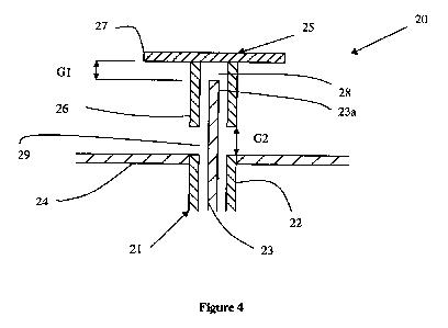
Figure 4 illustrates a cross section schematic representation of a preferred
embodiment
of the antenna arrangement 20 of the invention. In this arrangement a semi
rigid coaxial
feed 21 comprises an outer case 22 and an inner wire 23. The outer case 22 is
connected to a ground plane 24. The inner wire 23 extends above the ground
plane 24
to act as a conductive core 23a. The conductive core 23a is located
concentrically within
a cylindrical conductive case 26 and is configured as a second semi rigid
coaxial section
25. The second semi rigid coaxial section 25 further comprises a top loaded
disk 27. A
dielectric material 28 is located within the inner volume of the second semi
rigid coaxial
section 25. In this embodiment the dielectric material 28 is PTFE. A gap G1 is
provided between the top loaded disk 27 and the end of conductive core 23a. A
gap G2
is provided between the cylindrical conductive case 26 and the ground plane
24. A
dielectric material 29 is provided between the cylindrical conductive case 26
and the
ground plane 24. In this particular embodiment the dielectric material is air.
For experimental measurements the following dimensions were used for the
antenna
arrangement. The "top-hat" or disk is 24 mm in diameter, and acts as a short
circuit
plate on a section of coaxial transmission line 16 mm in length. The coaxial
transmission line has a Teflon inner (Cr = 2. 1, tan 6 = 0.000 1.) of 7 mm in
diameter and is
fed from another coaxial line entering from the ground plane. The inner wire
of this
transmission line extends 19 mm in length above the ground plane.
Figure 5 illustrates the return loss response of the preferred antenna
arrangement in
accordance with the invention shown in Figure 4. Figure 5 shows the measured
return
loss for antenna arrangement as a function of distance between the lowest
point of the
cylindrical conductive case 26 and the ground plane 24. The antenna
demonstrates a
return loss less than 10dB over the frequency band 2.1-5.1 GHz (or VSWR <_
1.92:1
over a 2.3:1 bandwidth) a 3 fold improvement when compared to a conventional
wideband X/4 disk loaded monopole (see figure 2). The feed was experimentally
optimised for matching bandwidth by adjusting the gap G2 (refer to Figure 4
set up) to
CA 02763850 2011-11-29
WO 2010/142946 PCT/GB2010/001116
around 6.5 mm. The laboratory prototype and their packaged duplicates indicate
the
electrical performance was reproducible and that ruggedisation of the design
for outdoor
use is feasible.
Figures 6 to 10 show the radiation patterns of the preferred antenna
arrangement as
measured at five different frequencies of 2.4, 3.0, 3.6, 4.2, and 4.8 GHz. The
antenna
radiation pattern is consistent with that intuitively expected i.e. a dipole
pattern with
radiation maximum on the horizontal plane. The principle E-plane co-
polarization and
cross-polarization field patterns were measured in an indoor anechoic chamber
over
+90 to -90 at the five frequencies already described. The results, shown in
Figures 6-
10, indicate that the antenna arrangement has excellent omni-directional
performance
with low cross-polarization (S 15 dB). Dips in the co-polar field patterns at
the centre
frequency of 3.6 GHz indicate the onset of side-lobes. The presence of side-
lobes is
anticipated from the wavelength in relative proportion to the dimension of the
disk.
There are techniques known in the art which can be applied to reduce side
lobes at the
expense of introducing loss.
Figure 11 shows the computer modelled results measured for gain versus
frequency for
the antenna arrangement shown in Figure 4, modelled in HFSS. The gain is
negative
below 800 MHz, with gain plateau of 5 dB from 1.8-4.0 GHz. Above 5 GHz the
antenna arrangement shows some resonant gain behaviour. The gain is consistent
with
the electrical size of the antenna as a function of frequency.
CA 02763850 2011-11-29
WO 2010/142946 PCT/GB2010/001116
I1
Table 1 shows laboratory measurements of gain at frequencies of 2.1, 3.5, and
4.8 GHz
for the preferred antenna arrangement. They are consistent with the HFSS
results of Fig.
11.
Frequency [GHz] Antenna Gain [dBJ
2.1 4.5
3.5 4.8
4.8 5.1
Table 1
The experimental Wheeler cap technique was used to measure radiation
efficiency for
the antenna arrangement of Figure 4. This measurement is accomplished by
placing the
antenna within a sealed shielded metal enclosure that shorts out far-field
radiation but
does not significantly perturb the near-field. A "metal cap" was constructed
from
aluminium to behave as a short section of circular waveguide. The cylindrical
diameter
was 50 cm and height 30cm. The antenna efficiency rl can be calculated using
equation
(1), where RF,.eeSpace is the input resistance without the metal cap on and
Rc,,p is the input
resistance with the metal cap placed over the antenna:
RFreespace - "Cap x100%O (1 )
RFreeSpace
The efficiency for the antenna arrangement of figure 4 was found to be around
95 1 %
at 2.3 GHz.
Figures 1.2 and 13, show the physical circuit representation and the
equivalent circuit
representation of the antenna arrangement of Figure 4 respectively. The key
design
feature to wideband performance is a double tuned circuit response achieved by
varying
G I G2 (refer to Figure 4 set up), dielectric materials and the ratio of core
radius to case
CA 02763850 2011-11-29
WO 2010/142946 PCT/GB2010/001116
12
radius. The person skilled in the art of antenna design will understand how
variation of
these parameters can be used to optimise the double tuned circuit response.The
final
performance rests on the choice of wideband resonant matching network and
keeping
the matching networks close to or ideally integral with the antenna (load).
Double tuned
resonant circuit responses were developed for the antenna arrangement of
Figure 4.
The approximate value for some of the circuit elements has been calculated
using the
following expressions, where constants have their usual meaning and r and h
are related
to the antenna geometry shown in Fig. 12.
Ca =co ur2lh. (2)
Ca is the internal capacitance of the simple disk loaded monopole.
Ce=eor 8+ 21n 1+0.8(r /11)2 +(0.31r/h)`` (3)
3 1+0.9(r/h)
Ce is the external fringing field capacitance of the disk loaded monopole,
Rr = 40(2irh / 2)2 (4)
Where Rr is the radiation resistance in the axial wire of a small antenna.
G=w2(Ce+C(1)`Rr (5)
G is a parallel conductance term that takes account of the frequency
dependence of Rr
and
Ra=60h (6)
r
CA 02763850 2011-11-29
WO 2010/142946 PCT/GB2010/001116
13
Ra is the equivalent aperture loading resistance.
La = GRa (7)
w2Ce
While La is the value of inductance across the resistance to give the
appropriate
frequency variation. The coaxial feed was modelled as a distributed short
circuited
coaxial component since its equivalent frequency variation would be more
exactly
followed. The circuit was simulated using the commercial software Ansoft
Designer
(available from Ansoft) and Figure 14 shows a comparison of measurement with
theory.
Clearly the double tuned circuit response is present in both the measurement
and circuit
model; though skewed in the higher frequency. It should be noted that the
calculated
values of lumped reactance values provide only approximate or "first order"
values
allowing an initial dimensioning and design of antenna arrangement of Figure
4.
Figure 15 shows a cross sectional illustration of the preferred invention
embodiment of
figure 4 with rectangular spatial polarisation fins 30. The common features of
Figure 4,
the outer case 22, ground plane 24, conductive core 23a, cylindrical
conductive case 26
and top loaded disk 27 are indicated. The fins 30 surround the antenna
arrangement at
regular angular intervals and are constructed of a High Impedance Surface in a
radial
arrangement around the centre of the antenna.
Figure 16 shows a cross sectional illustration of the preferred antenna
arrangement in a
linear array of three antenna. The common features of Figure 4, the ground
plane 24 and
top loaded disk 27 are indicated. The gap G I is varied to provide a very
broad stepped
bandwidth.