Note : Les descriptions sont présentées dans la langue officielle dans laquelle elles ont été soumises.
CA 02766363 2012-01-30
CONNECTOR FOR MULTIPLE INTERFACE CONNECTION STANDARDS
CROSS REFERENCE TO RELATED APPLICATION
[00011 This application is related to and claims priority benefits from U.S.
Provisional Application Serial No. 61/438,140, filed on January 31, 2011,
entitled
UNIVERSAL USB 1, 2, 3, ESATA I, 11, 111 CONNECTOR. The `140 application is
hereby
incorporated herein in its entirety by this reference.
FIELD OF THE INVENTION
[00021 The invention relates to mobile storage devices and the like.
BACKGROUND
100031 Universal Serial Bus ("USB") and External Serial Advanced Technology
Attachment ("eSATA") are two types of commonly used standards for connectors.
Each of
these standards have undergone rapid development since their inception.
100041 The USB standard that governs the design of the USB connections has
undergone several revisions since its earliest release in 1994. The first
widely adopted
version, USB 1.1, specified data rates of 1.5 Mbit/s ("Low-Bandwidth") and 12
Mbit/s
("Full-Bandwidth"). USB 1.1 was replaced by USB 2.0 in 2000. USB 2.0 provided
a higher
maximum data transfer rate of 480 Mbit/s ("Hi-Speed"). In this version, the
USB 2.0 cable
has four wires: two wires for power (+5 volts and ground) and a twisted pair
of wires for
carrying data. In the USB 2.0 design, as well as USB 1.1, data is transmitted
in one direction
at a time (downstream or upstream).
100051 In 2008, a new USB 3.0 standard was announced. USB 3.0 includes a new
"SuperSpeed" bus, which provides a fourth data transfer rate of 5.0 Gbit/s. In
order to
achieve this increased throughput, the USB 3.0 cable has a total of eight
wires: two wires for
power (+5 volts and ground), the twisted pair for carrying non-SuperSpeed data
(allows
I
CA 02766363 2012-01-30
backward compatibility with earlier versions of USB devices), and two
differential pairs for
carrying SuperSpeed data. Full-duplex signaling occurs over the two
differential pairs. To
date, adoption of the USB 3.0 standard has been slow due to the need to re-
design
motherboard hardware that supports the USB 3.0 standard, and the need to
revise operating
systems to support the USB 3.0 standard.
[0006] Traditionally, SATA is an internal computer bus interface for
connecting host
bus adapters to mass storage devices. First generation SATA interfaces ("SATA
I") specified
data transfer rates 1.5 Gbit/s. Second generation SATA interfaces ("SATA I I")
specified data
rates of 3.0 Gbit/s. All SATA data cables meeting the SATA spec are rated for
3.0 Gbit/s. In
2009, the third generation SATA interface ("SATA III") was released,
specifying a peak
throughput of 6 Gbit/s. The SATA III standard is backwards compatible with
SATA II.
eSATA was standardized in 2004 and provides a variant of the SATA protocols
for external
connectively. In each version of eSATA ("eSATA I", "eSATA 11", and "eSATA
Ill"), the
hardwire includes two differential pairs of wires, plus an additional three
ground wires.
Because eSATA uses the same ATA protocol as a computer's internal hard drive,
a bridge
chip is not needed to translate from the computer's internal ATA protocol to
another
protocol, such as USB. However, while most computers use SATA standards
internally,
many computers do not include external SATA connectors, opting instead to
include external
USB connectors.
100071 Because eSATA connectors are not yet widely available, it is desirable
to
provide eSATA connectors that include full backward and forward compatibility
between the
SATA I, 11, and III standards, in combination with USB connectors that include
full
backward and forward compatibility between the USB 2.0 and 3.0 standards.
2
CA 02766363 2012-01-30
SUMMARY
100081 Embodiments of the invention may comprise a connector having a
substrate, a
first interface connection terminal set electrically coupled to the substrate,
a second interface
connection terminal set electrically coupled to the substrate, a third
interface connection
terminal set electrically coupled to the substrate, a housing coupled to the
substrate and
surrounding at least a portion of the first interface connection terminal set,
the second
interface connection terminal set, and the third interface connection terminal
set, and a shell
coupled to the housing and the substrate, wherein the first interface
connection terminal set
and the second interface connection terminal set are configured to support at
least two
interface connection standards with interfaces that are mechanically
different. In certain
embodiments, the shell is metal.
[00091 In some embodiments, the first interface connection terminal set
comprises a
plurality of connection fingers. The second interface connection terminal set
may comprise a
plurality of springs. In certain embodiments, the substrate comprises a
plurality of apertures,
wherein each of the plurality of springs of the second interface connection
terminal set are
partially enclosed within each of the plurality of apertures. The third
interface connection
terminal set may comprise a plurality of springs. In some embodiments, the
housing
comprises a plurality of channels, wherein each of the plurality of springs of
the third
interface connection terminal set are partially enclosed within each of the
plurality of
channels.
[00101 In some embodiments, a recess is positioned between a lower surface of
the
housing and a component surface of the substrate. At least one controller may
also be
electrically coupled to the substrate. The controller may be at least
partially surrounded by
the housing and/or may be positioned within a recess, which is positioned
between a lower
surface of the housing and a component surface of the substrate.
3
CA 02766363 2012-01-30
BRIEF DESCRIPTION OF THE DRAWINGS
[0011] Figure 1 is a front perspective view of a connector according to
certain
embodiments of the present invention.
100121 Figure 2 is a rear perspective view of the connector of Figure 1.
100131 Figure 3 is an exploded front perspective view of the connector of
Figure 1.
100141 Figure 4 is a front perspective view of the connector of Figure 1 with
the shell
removed.
[00151 Figure 5 is a front perspective view of the connector of Figure 1 with
the shell,
housing, and third interface connectors removed.
[00161 Figure 6 is a front perspective view of a second interface connection
terminal
set of the connector of Figure 1.
100171 Figure 7 is a front perspective view of a third interface connection
terminal set
of the connector of Figure 1.
[0018] Figure 8 is a bottom plan view of the connector of Figure 1.
100191 Figure 9 is a cross-sectional view of the connector of Figure 1 taken
along line
9-9.
[0020] Figure 10 is a cross-section view of the connector of Figure 9 with a
controller
added.
100211 Figure 1 1 is a front perspective view of a connector according to
alternative
embodiments of the present invention.
100221 Figure 12 is a front perspective view of a connector according to
alternative
embodiments of the present invention.
DETAILED DESCRIPTION
[00231 The described embodiments of the invention provide connectors for use
with
multiple interface connection standards. While the designs may be discussed
for use with
4
CA 02766363 2012-01-30
eSATA and USB standards, they are by no means so limited. Rather, embodiments
of these
designs may be used for other devices that couple to any type of serial bus
connection,
parallel bus connection, or otherwise as desired.
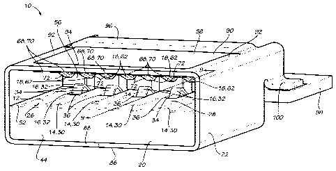
100241 Figures 1-12 illustrate embodiments of a connector 10 with multiple
interface
connection standards. In the embodiments shown in Figures 1-12, the connector
10
comprises a substrate 12, a first interface connection terminal set 14, a
second interface
connection terminal set 16, a third interface connection terminal set 18, a
housing 20, and a
shell 22.
100251 As best shown in Figures 1-5 and 8-12, the substrate 12 may be a
printed
circuit board ("PCB"), which is used to mechanically support and electrically
connect the
first interface connection terminal set 14, the second interface connection
terminal set 16, and
the third interface connection terminal set 18 to other components that may be
mounted to the
substrate 12. In some embodiments, the substrate 12 may include a component
surface 24
and a connection surface 26. Items such as an oscillator, an LED status light,
discrete
components, or other suitable devices, may be mounted and electrically coupled
to the
component surface 24 and/or the connection surface 26.
100261 In some embodiments, as illustrated in Figures 1 and 3-5, the first
interface
connection terminal set 14 may be positioned proximate an end 28 of the
substrate 12 and
configured to be inserted within corresponding connector using the first
interface connection
standard. In some embodiments, such as the embodiments illustrated in Figures
1 and 3-5,
the first interface connection terminal set 14 may comprise a plurality of
connection fingers
30. In these embodiments, the connection fingers 30 may be mounted to or
embedded within
the connection surface 26 of the substrate 12 and electrically coupled to the
substrate 12. In
certain embodiments, such as where the first interface connection standard is
a USB 2.0
standard or any other standard that is forward or backwards compatible with
the USB 2.0
CA 02766363 2012-01-30
standard, the connection fingers 30 may be configured to electrically couple
to the power and
ground wires and the twisted pair of wires (for Hi-Speed and lower data
transfer) of the
corresponding USB 2.0 connector when the connector 10 is inserted within the
corresponding
USB 2.0 connector. In the embodiments shown in Figures I and 3-5, the first
interface
connection terminal set 14 may comprise four connection fingers 30. However,
one of
ordinary skill in the relevant art will understand that any suitable number
and configuration of
connection fingers 30 may be used in conjunction with the first interface
connection standard
or other suitable standards.
[00271 In some embodiments, as illustrated in Figures 1, 3-5, and 9-10, the
second
interface connection terminal set 16 may be positioned proximate the end 28 of
the substrate
12, as well as behind and/or proximate the first interface connection terminal
set 14, and
configured to be inserted within a corresponding connector using the second
interface
connection standard. In some embodiments, such as the embodiment illustrated
in Figures 1,
3-5, and 9-10, the second interface connection terminal set 16 may comprise a
plurality of
contact springs 32. Each spring 32 may be formed of a resilient material that,
when bent or
compressed, exerts a force to return to its original shape. One of ordinary
skill in the relevant
art will understand that the springs 32 may be made of any suitable material
and have any
suitable design that allows the second interface connection terminal set 16 to
electrically
couple to the corresponding connector when the connector 10 is inserted within
the
corresponding connector. In certain embodiments, such as where the second
interface
connection standard is a USB 3.0 standard or any other standard that is
forward or backwards
compatible with the USB 3.0 standard, the springs 32, in combination with the
connection
fingers 30, may be configured to electrically couple to the power and ground
wires, the
twisted pair of wires (for Hi-Speed and lower data transfer), and the two
differential pairs of
wires (for SuperSpeed data transfer) of the corresponding USB 3.0 connector
when the
6
CA 02766363 2012-01-30
connector 10 is inserted within the corresponding USB 3.0 connector. In the
embodiments
shown in Figures 3 and 5-6, the second interface connection terminal set 16
may comprise
five springs 32. However, one of ordinary skill in the relevant art will
understand that any
suitable number and configuration of springs 32 may be used in conjunction
with the second
interface connection standard or other suitable standards.
[00281 Each spring 32 may also include a coupling projection 34, as best
illustrated in
Figures 1, 4-5, and 9-10. In some embodiments, the coupling projection 34 may
be integrally
formed with the spring 32. In other embodiments, the coupling projection 34
may be
soldered or otherwise electrically coupled to the spring 32 in a suitable
manner that allows
the coupling projection 34 to be electrically coupled to the substrate 12. The
coupling
projection 34 may have any suitable shape that provides sufficient contact
with the
corresponding connector when the connector 10 is inserted within the
corresponding
connector. Examples of suitable shapes include but are not limited to a
triangular, L-shape,
U-shape, T-shape, solid projection having a circular or rectilinear cross-
sectional shape, or
other suitable shapes.
100291 The substrate 12 may include a plurality of apertures 36 in the
connection
surface 26 adjacent the plurality of springs 32. The plurality of apertures 36
may be shaped
so that the coupling projection 34 of each spring 32 extends through the
aperture 36 and is
positioned above the connection surface 26, while the remainder of the spring
32 body is
positioned within the substrate 12, when each spring 32 is in an uncompressed
position.
[00301 Each spring 32 may include an extension 38 that mounts to and
electrically
couples the spring 32 to the substrate 12 via a coupling point 40 located on
the connection
surface 26. The substrate 12 may include a separate coupling point 40 for each
spring 32. In
some embodiments, as shown in Figures 3, 5-6, and 9-10, the extension 38 may
have a U-
shape configuration that is shaped to extend above the aperture 36 and over a
portion of the
7
CA 02766363 2012-01-30
substrate 12, then return to the connection surface 26 of the substrate 12
adjacent the coupling
point 40. An end 42 of the extension 38 may be soldered or otherwise
electrically coupled to
the coupling point 40 in a suitable manner that allows each coupling
projection 34 to be
electrically connected to the corresponding coupling point 40.
100311 The coupling points 40 may be mounted to or embedded within the
connection
surface 26 of the substrate 12 and electrically coupled to the substrate 12.
In these
embodiments, the coupling points 40 may be positioned behind and/or adjacent
the apertures
36. In other embodiments, the coupling points 40 may be mounted to or embedded
within the
component surface 24, while the connection fingers 30 may be mounted to or
embedded
within the connection surface 26, or vice versa. One of ordinary skill in the
relevant art will
understand that the coupling points 40 may be positioned in any suitable
location on the
substrate 12 that allows the second interface connection terminal set 16 to
electrically couple
to the substrate 12.
[00321 In some embodiments, when the connector 10 is inserted within the
corresponding connector (not shown), the corresponding connector presses
against the
coupling projections 34, in turn applying a compressive force to the springs
32. When the
springs 32 are compressed by the corresponding connector, the spring-loaded
design of each
spring 32 then applies a force to create a firm electrical coupling between
the corresponding
connector and each coupling projection 34 when the connector 10 is inserted
within the
corresponding connector.
[00331 The housing 20 may be coupled to the substrate 12 proximate the end 28.
The
shell may be formed of composite materials, plastic materials, or other
suitable materials.
The housing 20 may comprise a front wall 44 and side walls 46 that are joined
to form a U-
shaped frame that substantially surrounds at least a portion of a front
surface 48 and side
surfaces 50 of the end 28. In some embodiments, the side walls 46 may have
substantially
8
CA 02766363 2012-01-30
the same height as or may have a greater height than the side surfaces 50, and
the front wall
44 may have substantially the same height as or may have a greater height than
the front
surface 48. In the embodiments shown in Figures 3-4 and 9-10, upper edges 52
of the front
wall 44 and the side walls 46 are substantially aligned with the connection
surface 26. In
these embodiments, lower edges 54 of the front wall 44 and the side walls 46
extend below
the front surface 48 and the side surfaces 50.
[00341 As illustrated in Figures 1-4 and 9-10, a rear wall 56 may be coupled
to a
portion of the upper edges 52 of the side walls 46. The rear wall 56 may be
configured to
extend across the connection surface 26 behind and/or adjacent the apertures
36. An upper
platform 58 may be coupled to a portion of a front surface 59 of the rear wall
56, wherein the
upper platform 58 extends over the end 28 of the substrate 12, but is spaced
apart from the
end 28 by the height of the rear wall 56.
[00351 In some embodiments, as illustrated in Figures 1, 3-4, 7, and 9-10, the
third
interface connection terminal set 18 may be positioned proximate an interior
surface 60 of the
upper platform 58 and configured to be inserted within a corresponding
connector using the
third interface connection standard. In some embodiments, such as the
embodiment
illustrated in Figures 1, 3-4, 7, and 9-10, the third interface connection
terminal set 18 may
comprise a plurality of contacts 62. In certain embodiments, such as where the
third interface
connection standard is an eSATA I, eSATA 11, eSATA Ill, or any other standard
that is
forward or backwards compatible with any of the foregoing eSATA standards, the
contacts
62 may be mounted to or embedded within the interior surface 60 of the upper
platform 58
and configured to electrically couple to the two differential pairs of wires,
plus an additional
three ground wires, of the corresponding eSATA connector when the connector 10
is inserted
within the corresponding eSATA connector. In the embodiments shown in Figures
1, 3, and
7, the third interface connection terminal set 18 comprises seven contacts 62.
However, one
9
CA 02766363 2012-01-30
of ordinary skill in the relevant art will understand that any suitable number
and configuration
of contacts 62 may be used in conjunction with the third interface connection
standard or
other suitable connection standards.
100361 Each contact 62 may include a main body 64 and a spring 66, as best
illustrated in Figures 3 and 7. Each spring 32 may be formed of a resilient
material that,
when bent or compressed, exerts a force to return to its original shape. One
of ordinary skill
in the relevant art will understand that the springs 32 may be made of any
suitable material
and have any suitable design that allows the third interface connection
terminal set 18 to
electrically couple to the corresponding connector when the connector 10 is
inserted within
the corresponding connector. In some embodiments, as shown in Figures 1 and 4,
the main
body 64 of each contact 62 may be positioned within a corresponding channel 68
located on
the interior surface 60 of the upper platform 58, so that the interior surface
60 includes a
plurality of channels 68. The main body 64 may be coupled to the spring 66
adjacent a front
edge 70 of the channel 68. In some embodiments, the channel 68 is shaped so
that the spring
66 may be positioned alongside the main body 64 within the channel 68.
100371 Each spring 66 may also include a coupling projection 72, as best
illustrated in
Figures 1, 4, and 9-10. In some embodiments, the coupling projection 72 may be
integrally
formed with the spring 66. In other embodiments, the coupling projection 72
may be
soldered or otherwise electrically coupled to the spring 66 in a suitable
manner that allows
the coupling projection 72 to be electrically coupled to the substrate 12. The
coupling
projection 72 may have any suitable shape that provides sufficient contact
with the
corresponding connector when the connector 10 is inserted within the
corresponding
connector. Examples of suitable shapes include but are not limited to a
triangular, L-shape,
U-shape, T-shape, solid projection having a circular or rectilinear cross-
sectional shape, or
other suitable shapes.
CA 02766363 2012-01-30
100381 The channels 68 may be shaped so that the coupling projection 72 of
each
spring 66 extends through the channel 68 and is positioned below the interior
surface 60,
while the remainder of the spring 66 is positioned within the channel 68, when
each spring 66
is in an uncompressed position.
100391 Each main body 64 may include an extension 74 that mounts to and
electrically couples the spring 66 to the substrate 12 via a coupling point 76
located on the
connection surface 26. The substrate 12 may include a separate coupling point
76 for each
spring 66, as best shown in Figure 2. In some embodiments, as shown in Figures
3 and 7, the
extension 74 may have an L-shape configuration that is shaped to extend down
from the
upper platform 58 and over a portion of connection surface 26 of the substrate
12 adjacent the
coupling point 76. An end 78 of the extension 74 may be soldered or otherwise
electrically
coupled to the coupling point 76 in a suitable manner that allows each
coupling projection 72
to be electrically connected to the corresponding coupling point 76.
[00401 The coupling points 76 may be mounted to or embedded within the
connection
surface 26 of the substrate 12 and electrically coupled to the substrate 12.
In these
embodiments, the coupling points 76 may be positioned behind and/or adjacent
the apertures
36, as well as adjacent the coupling points 40. In other embodiments, the
coupling points 76
may be mounted to or embedded within the component surface 24, while the
connection
fingers 30 and/or the coupling points 40 may be mounted to or embedded within
the
connection surface 26, or vice versa. One of ordinary skill in the relevant
art will understand
that the coupling points 76 may be positioned in any suitable location on the
substrate 12 that
allows the third interface connection terminal set 18 to electrically couple
to the substrate 12.
100411 When the connector 10 is inserted within the corresponding connector
(not
shown), the corresponding connector presses against the coupling projections
72, in turn
applying a compressive force to the springs 66. When the springs 66 are
compressed by the
11
CA 02766363 2012-01-30
corresponding connector, the spring-loaded design of each spring 66 then
applies a force to
create a firm electrical coupling between the corresponding connector and each
coupling
projection 72 when the connector 10 is inserted within the corresponding
connector.
[0042] While in some embodiments, the first, second, and third interface
connection
standards may be a USB 2.0 standard, a USB 3.0 standard, and/or an eSATA I,
eSATA II,
eSATA III (or any other standard that is forward or backwards compatible with
any of the
foregoing standards), one of ordinary skill in the relevant art will
understand that the three
interface connection standards may be any suitable combination of interface
connection
standards that achieve the desired performance of the connector 10.
[0043] The rear wall 56 may include apertures 80 shaped to allow the
extensions 38,
74 to pass through the rear wall 56, which may otherwise form a barrier
between the springs
32, 66 and the coupling points 40, 76.
[0044] A lower surface 82 may be coupled to the lower edges 54 of the front
wall 44
and the side walls 46 of the housing 20, forming a partially enclosed recess
84 between the
component surface 24 of the substrate 12 and the lower surface 82. The recess
84 may
provide a space for at least one controller 86 to be mounted to or embedded
within the
component surface 24 of the substrate 12 and electrically coupled to the
substrate 12.
Specifically, in some embodiments, the controller 86 may be designed as a
surface mount
device ("SMD") part, which makes it possible to mount the connector easily and
does not
require the presence of holes in the substrate 12. By locating the controller
86 within the
connector 10, the connector 10 design conserves space and allows for the use
of very short
signal lines between the first interface connection terminal set 14, the
second interface
connection terminal set 16, and/or the third interface connection terminal set
18, resulting in
better signals and higher transmission speed.
12
CA 02766363 2012-01-30
[0045] The shell 22 may then be coupled to the housing 20 and the substrate
12. The
shell may be formed of metallic materials, composite materials, plastic
materials, or other
suitable materials. The shell 22 is shaped to wrap around at least a portion
of the outer shape
of the housing 20. Edges 88 of the shell 22 may be joined below the lower
surface 82 of the
housing 20, as shown in Figure 8. In certain embodiments, the shell 22
comprises an opening
90 that is positioned adjacent the upper platform 58. The opening 90 is
surrounded by sides
92, a front edge 94, and a rear bridge 96. In other embodiments, as shown in
Figure 12, the
rear bridge 96 may be eliminated to reduce weight and costs.
[0046] In some embodiments, as shown in Figures 1-5, 8, and 12, the substrate
12
may be shaped so that the end 28 has a narrower width than a remaining portion
98 of the
substrate 12. Thus, the remaining portion 98 extends outwardly past the side
walls 46 of the
housing 20. In these embodiments, the shell 22 may include tabs 100 that are
shaped to
couple to the remaining portion 98 adjacent and outside the side walls 46 of
the housing 20.
[0047] In other embodiments, as shown in Figure 11, the substrate 12 has the
same
width in the remaining portion 98 and the end 28. In these embodiments, the
shell 22 may
include tabs 102 that are shaped to couple to the side surfaces 50 adjacent
the side walls 46 of
the housing 20.
[0048] The foregoing is provided for purposes of illustrating, explaining, and
describing embodiments of the present invention. Further modifications and
adaptations to
these embodiments will be apparent to those skilled in the art and may be made
without
departing from the scope or spirit of the invention.
13