Note : Les descriptions sont présentées dans la langue officielle dans laquelle elles ont été soumises.
CA 02766636 2012-02-07
COATING FOR IMPROVED WEAR RESISTANCE
FIELD OF THE INVENTION
The present invention relates to coatings and, in particular, to coatings
deposited
by physical vapor deposition (PVD).
BACKGROUND
Cutting tools, including cemented carbide cutting tools, have been used in
both
coated and uncoated conditions for machining various metals and alloys. In
order to
increase cutting tool wear resistance and lifetime, one or more layers of
refractory
materials have been applied to cutting tool surfaces. TiC, TiCN, TiN and
A12O3, for
example, have been applied to cemented carbide substrates by chemical vapor
deposition
(CVD). Moreover, in recognizing some shortcomings of CVD coatings related to
specific cutting applications, cutting tool manufacturers have also provided
refractory
coatings applied by PVD. TiN coatings applied by PVD, for example, have been
generally accepted in the cutting tool community.
One disadvantage of TiN coatings is the susceptibility to oxidation at
relatively
low temperatures. TiN coatings, for example, demonstrate oxidation beginning
at about
550 C. As a result, aluminum has been added to TiN coatings in efforts to
increase the
oxidation resistance. Silicon has additionally been added to TiN coatings to
increase
oxidation resistance. However, the addition of silicon to TiN and/or TiA1N
coatings can
induce significant stresses in the coatings thereby inducing premature coating
failure by
delamination from the cutting tool surface.
United States Patent 6,586,122 addresses methods of incorporating silicon into
TiN and TiA1N coatings to increase oxidation resistance while reducing
residual
compressive stresses of the coatings. The synthetic methods disclosed in
United States
Patent 6,586,122 induce a phase separated coating wherein a high silicon
concentration
Si3N4 nanophase is dispersed throughout a low silicon concentration TiSiN
matrix phase.
Dispersing a high silicon concentration Si3N4 nanophase throughout a low
silicon
concentration matrix phase can reduce lattice strain induced by the
substitution of Ti with
Si in a TiN or TiAlSiN coating.
1
CA 02766636 2012-02-07
The synthetic methods required to induce such a phase separated coating,
nevertheless, are unconventional and require alteration of traditional PVD
methods
and/or equipment, thereby potentially limiting widespread application of the
methods and
increasing coated tool production costs.
SUMMARY
In one aspect, coated cutting tools are described herein which, in some
embodiments, can demonstrate improved wear resistance in one or more cutting
applications. In some embodiments, a coated cutting tool described herein
comprises a
substrate and a coating adhered to the substrate, the coating comprising an
inner layer
deposited by physical vapor deposition comprising aluminum and one or more
metallic
elements selected from the group consisting of metallic elements of Groups
IVB, VB and
VIB of the Periodic Table and one or more non-metallic elements selected from
the group
consisting of non-metallic elements of Groups IIIA, IVA and VIA of the
Periodic Table
and an outer layer deposited by physical vapor deposition over the inner
layer, the outer
layer comprising aluminum and silicon and one or more metallic elements
selected from
the group consisting of metallic elements of Groups IVB, VB and VIB of the
Periodic
Table and one or more non-metallic elements selected from the group consisting
of non-
metallic elements of Groups IIIA, IVA and VIA of the Periodic Table, wherein
the
amount of silicon in the outer layer decreases toward the inner layer.
In another aspect, a coated cutting tool described herein comprises a
substrate and
a coating adhered to the substrate, the coating comprising an inner layer
deposited by
physical vapor deposition comprising aluminum and one or more metallic
elements
selected from the group consisting of metallic elements of Groups IVB, VB and
VIB of
the Periodic Table and one or more non-metallic elements selected from the
group
consisting of non-metallic elements of Groups IIIA, IVA and VIA of the
Periodic Table
and an outer layer deposited by physical vapor deposition over the inner
layer. The outer
layer of the coating comprises a phase composed of aluminum and silicon and
one or
more metallic elements selected from the group consisting of metallic elements
of Groups
IVB, VB and VIB of the Periodic Table and one or more non-metallic elements
selected
from the group consisting of non-metallic elements of Groups IIIA, IVA and VIA
of the
2
CA 02766636 2012-02-07
Periodic Table and a phase composed of aluminum and silicon and one or more
non-
metallic elements selected from the group consisting of non-metallic elements
of Groups
IIIA, IVA and VIA of the Periodic Table.
In some embodiments, coatings described herein demonstrate residual
compressive stresses. In some embodiments, a coated cutting tool described
herein
comprises a substrate and a coating adhered to the substrate, the coating
comprising an
inner layer deposited by physical vapor deposition comprising aluminum and one
or more
metallic elements selected from the group consisting of metallic elements of
Groups IVB,
VB and VIB of the Periodic Table and one or more non-metallic elements
selected from
the group consisting of non-metallic elements of Groups IIIA, IVA and VIA of
the
Periodic Table and an outer layer deposited by physical vapor deposition over
the inner
layer, the outer layer comprising aluminum and silicon and one or more
metallic elements
selected from the group consisting of metallic elements of Groups IVB, VB and
VIB of
the Periodic Table and one or more non-metallic elements selected from the
group
consisting of non-metallic elements of Groups IIIA, IVA and VIA of the
Periodic Table,
wherein the coating has a residual compressive stress and/or compressive shear
stress.
In another aspect, methods of making coated cutting tools are described
herein.
In some embodiments, a method of making a coated cutting tool comprises
providing a
cutting tool substrate and depositing an inner layer of a coating on the
substrate by
physical vapor deposition, the inner layer comprising aluminum and one or more
metallic
elements selected from the group consisting of metallic elements of Groups
IVB, VB and
VIB of the Periodic Table and one or more non-metallic elements selected from
the group
consisting of non-metallic elements of Groups IIIA, IVA and VIA of the
Periodic Table.
An outer layer of the coating is deposited over the inner layer by physical
vapor
deposition, the outer layer comprising aluminum and silicon and one or more
metallic
elements selected from the group consisting of metallic elements of Groups
IVB, VB and
VIB of the Periodic Table and one or more non-metallic elements selected from
the group
consisting of non-metallic elements of Groups IIIA, IVA and VIA of the
Periodic Table,
wherein the amount of silicon in the outer layer is decreased toward the inner
layer.
In some embodiments, an outer layer is deposited over the inner layer by
physical
vapor deposition, the outer layer comprising a phase composed of aluminum and
silicon
3
CA 02766636 2012-02-07
and one or more metallic elements selected from the group consisting of
metallic
elements of Groups IVB, VB and VIB of the Periodic Table and one or more non-
metallic elements selected from the group consisting of non-metallic elements
of Groups
IIIA, IVA and VIA of the Periodic Table and a phase composed of aluminum and
silicon
and one or more non-metallic elements selected from the group consisting of
non-
metallic elements of Groups IIIA, IVA and VIA of the Periodic Table.
In another aspect, methods of increasing the cutting lifetime of a coated
cutting
tool are described herein. In some embodiments, a method of increasing the
cutting
lifetime of a coated cutting tool comprises directing one or more coating
fatigue
mechanisms to an interface of an inner layer and an outer layer of the coating
by
producing the inner layer from a composition deposited by physical vapor
deposition
comprising aluminum and one or more metallic elements selected from the group
consisting of metallic elements of Groups IVB, VB and VIB of the Periodic
Table and
one or more non-metallic elements selected from the group consisting of non-
metallic
elements of Groups IIIA, IVA and VIA of the Periodic Table and producing the
outer
layer from a composition deposited by physical vapor deposition comprising
aluminum
and silicon and one or more metallic elements selected from the group
consisting of
metallic elements of Groups IVB, VB and VIB of the Periodic Table and one or
more
non-metallic elements selected from the group consisting of non-metallic
elements of
Groups IIIA, IVA and VIA of the Periodic Table, wherein the amount of silicon
in the
outer layer decreases toward the inner layer.
In some embodiments, directing comprises initiating one or more coating
fatigue
mechanisms at an interface of the inner layer and the outer layer of the
coating.
These and other embodiments are described in greater detail in the detailed
description which follows.
BRIEF DESCRIPTION OF THE DRAWINGS
Figure 1 illustrates a substrate of a coated cutting tool according to one
embodiment described herein.
Figure 2 illustrates a glow discharge spectrum of a coated cutting tool
according
to one embodiment described herein.
4
CA 02766636 2012-02-07
Figure 3 illustrates a sectional view of the glow discharge spectrum of Figure
2.
Figure 4 illustrates an energy dispersive spectrum of a coating according to
one
embodiment described herein.
Figure 5 illustrates an X-ray diffractogram of a coated cutting tool according
to
one embodiment described herein.
Figure 6 illustrates a glow discharge spectrum of a post coat treated cutting
tool
according to one embodiment described herein.
Figure 7 is a sectional view of the glow discharge spectrum of Figure 6.
Figure 8 is an energy dispersive spectrum of a post coat treated coating
according
to one embodiment described herein.
Figure 9 is an X-ray diffractogram of a post coat treated cutting tool
according to
one embodiment described herein.
DETAILED DESCRIPTION
Embodiments described herein can be understood more readily by reference to
the
following detailed description and examples and their previous and following
descriptions. Elements, apparatus and methods described herein, however, are
not
limited to the specific embodiments presented in the detailed description and
examples.
It should be recognized that these embodiments are merely illustrative of the
principles of
the present invention. Numerous modifications and adaptations will be readily
apparent
to those of skill in the art without departing from the spirit and scope of
the invention.
In one aspect, coated cutting tools are described herein which, in some
embodiments, can demonstrate improved wear resistance in one or more cutting
applications. In some embodiments, a coated cutting tool described herein
comprises a
substrate and a coating adhered to the substrate, the coating comprising an
inner layer
deposited by physical vapor deposition comprising aluminum and one or more
metallic
elements selected from the group consisting of metallic elements of Groups
IVB, VB and
VIB of the Periodic Table and one or more non-metallic elements selected from
the group
consisting of non-metallic elements of Groups IIIA, IVA and VIA of the
Periodic Table
and an outer layer deposited by physical vapor deposition over the inner
layer, the outer
layer comprising aluminum and silicon and one or more metallic elements
selected from
5
CA 02766636 2012-02-07
the group consisting of metallic elements of Groups IVB, VB and VIB of the
Periodic
Table and one or more non-metallic elements selected from the group consisting
of non-
metallic elements of Groups IIIA, IVA and VIA of the Periodic Table, wherein
the
amount of silicon in the outer layer decreases toward the inner layer.
In another aspect, a coated cutting tool described herein comprises a
substrate and
a coating adhered to the substrate, the coating comprising an inner layer
deposited by
physical vapor deposition comprising aluminum and one or more metallic
elements
selected from the group consisting of metallic elements of Groups IVB, VB and
VIB of
the Periodic Table and one or more non-metallic elements selected from the
Group
consisting of non-metallic elements of Groups IIIA, IVA and VIA of the
Periodic Table
and an outer layer deposited by physical vapor deposition over the inner
layer. The outer
layer of the coating comprises a phase composed of aluminum and silicon one or
more
metallic elements selected from the group consisting of metallic elements of
Groups IVB,
VB and VIB of the Periodic Table and one or more non-metallic elements
selected from
the group consisting of non-metallic elements of Groups IIIA, IVA and VIA of
the
Periodic Table and a phase composed of aluminum and silicon and one or more
non-
metallic elements selected from the group consisting of non-metallic elements
of Groups
IIIA, IVA and VIA of the Periodic Table.
Turning now to components of a coated cutting tool described herein, a coated
cutting tool described herein comprises a substrate. A coated cutting tool
described
herein can comprise any substrate not inconsistent with the objectives of the
present
invention. In some embodiments, a substrate comprises a cemented carbide,
carbide,
ceramic, cermet or steel.
A cemented carbide substrate, in some embodiments, comprises tungsten carbide
(WC). In some embodiments, WC is present in a substrate in an amount of at
least about
70 weight percent. In some embodiments, WC is present in a substrate in an
amount of at
least about 80 weight percent or in an amount of at least about 85 weight
percent.
Additionally, in some embodiments, the binder of a cemented carbide substrate
comprises cobalt or cobalt alloy. Cobalt, in some embodiments, is present in a
cemented
carbide substrate in an amount ranging from about 3 weight percent to about 15
weight
percent. In some embodiments, cobalt is present in a cemented' carbide
substrate in an
6
CA 02766636 2012-02-07
amount ranging from about 5 weight percent to about 12 weight percent or from
about 6
weight percent to about 10 weight percent. In some embodiments, a cemented
carbide
substrate may exhibit a zone of binder enrichment beginning at and extending
inwardly
from the surface of the substrate.
A cemented carbide substrate, in some, embodiments, further comprises one or
more additives such as, for example, one or more of the following elements
and/or their
compounds: titanium, niobium, vanadium, tantalum, chromium, zirconium and/or
hafnium. In some embodiments, titanium, niobium, vanadium, tantalum, chromium,
zirconium and/or hafnium form solid solution carbides with the WC in the
substrate. The
substrate, in some embodiments, comprises one or more solid solution carbides
in an
amount ranging from about 0.1 weight percent to about 5 weight percent.
Additionally,
in some embodiments, a cemented carbide substrate comprises nitrogen.
In some embodiments, a substrate of a coated cutting tool described herein
comprises one or more cutting edges formed at the juncture of a rake face and
flank faces
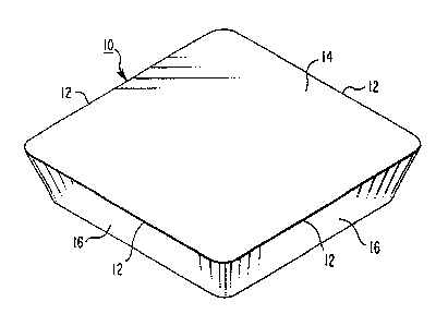
of the substrate. Figure 1 illustrates a substrate of a coated cutting tool
according to one
embodiment described herein. As illustrated in Figure 1, the substrate (10)
has cutting
edges (12) formed at the junction of the substrate rake face (14) and flank
faces (16).
In some embodiments, a substrate of a coated cutting tool can comprise an
insert,
drill bit, saw blade or other cutting apparatus.
As described herein, a coating adhered to the substrate comprises a inner
layer
deposited by physical vapor deposition comprising aluminum and one or more
metallic
elements selected from the group consisting of metallic elements of Groups
IVB, VB and
VIB of the Periodic Table and one or more non-metallic elements selected from
the group
consisting of non-metallic elements of Groups IIIA, IVA and VIA of the
Periodic Table.
Groups of the Periodic Table described herein are identified according to the
CAS
designation.
In some embodiments, one or more metallic elements of Groups IVB, VB and
VIB suitable for combination with aluminum in the production of an inner layer
of a
coating described herein comprise titanium, zirconium, hafnium, vanadium,
niobium,
tantalum and/or chromium. Moreover, in some embodiments, one or more non-
metallic
elements of Groups IIIA, IVA and VIA suitable for use in the production of an
inner
7
CA 02766636 2012-02-07
layer of a coating described herein comprise boron, carbon, nitrogen and/or
oxygen. In
some embodiments, an inner layer of a coating described herein has a
composition
according to the following relationship:
(Ala Zrb Hff Vd Nbe Taf Crg Ti1_(a+b+c+d+e+f+g))(OXCyN1_(x+y)), wherein 0<a<l,
0<b<l,
0<c<1, 0<d<1, 0<e<l, 0<f<1, 0<g<1, 0<x<l, 0<y<1 and (a + b + c + d + e + f+ g)
< 1
and (x + y) < 1.
In some embodiments, an inner layer of a coating described herein has a
composition according to the following relationship: AlaTi1_aN wherein D<a<l.
In some
embodiments of an inner layer having the composition AlaTi1_aN, 0.3 < a:5 0.8.
In some
embodiments, 0.35 < a < 0.75. In some embodiments, 0.4 < a < 0.7 or 0.42 < a.-
5 0.65.
In some embodiments, AlaTi1_aN of an inner layer of a coating described herein
is
in the crystalline phase. AlaTi1_aN of an inner layer, in some embodiments,
displays a
cubic crystalline structure. In some embodiments, the cubic crystalline
structure of
AlaTi1_aN of an inner layer is face centered cubic (fcc). In some embodiments,
AlaTi1_aN
of an inner layer displays a hexagonal crystalline structure. In some
embodiments,
AlaTi1_aN of an inner layer displays a mixture of cubic crystalline structure
and hexagonal
crystalline structure.
Moreover, in some embodiments, an inner layer of a coating described herein is
polycrystalline having an average crystallite size of at least about 10 nm. In
some
embodiments, an inner layer of a coating has an average crystallite size of at
least about
20 nm or at least about 50 nm. In some embodiments, an inner layer of a
coating has an
average crystallite size ranging from about 10 nmto about 100 nm or from about
20 nm
to about 80 nm. An inner layer of a coating, in some embodiments, has an
average
crystallite size ranging from about 30 nm to about 70 nm. In some embodiments,
an
inner layer of a coating has an average crystallite size greater than 100 nm.
An inner layer of a coating described herein can have any desired thickness
not
inconsistent with the objectives of the present invention. In some
embodiments, an inner
layer of a coating has a thickness ranging from about 1 m to about 10 m. In
some
embodiments, an inner layer has a thickness ranging from about 2 m to about 8
m or
from about 3 m to about 7 m. In some embodiments, an inner layer has a
thickness
ranging from about 1.5 m to about 5 m or from about 2 m to about 4 m. In
some
8
CA 02766636 2012-02-07
embodiments, an inner layer of a coating has a thickness less than about 1 m
or greater
than about 10 m.
As described further herein, an inner layer of a coating, in some embodiments,
is
deposited directly on a surface of the cutting tool substrate by physical
vapor deposition.
Alternatively, in some embodiments, one or more additional layers may be
disposed
between a surface of the substrate and the inner layer such that the inner
layer is not in
direct contact with the surface of the substrate.
A coating described herein also comprises an outer layer deposited by physical
vapor deposition over the inner layer, the outer layer comprising aluminum and
silicon
and one or more metallic elements selected from the group consisting of
metallic
elements of Groups IVB, VB, and VIB of the Periodic Table and one or more non-
metallic elements selected from the group consisting of non-metallic elements
of Groups
IIIA, IVA and VIA of the Periodic Table, wherein the amount of silicon in the
outer layer
decreases toward the inner layer.
In some embodiments, one or more metallic elements of Groups IVB, VB and
VIB suitable for combination with aluminum and silicon in the production of an
outer
layer of a coating described herein comprise titanium, zirconium, hafnium,
vanadium,
niobium, tantalum and/or chromium. Moreover, in some embodiments, one or more
non-
metallic elements of Groups IIIA, IVA and VIA suitable for use in the
production of an
outer layer of a coating described herein comprise boron, carbon, nitrogen
and/or oxygen.
In some embodiments, an outer layer of a coating described herein has a
composition
according to the following relationship:
(Alm Zrn Hfo VP Nbq Tai Cr, Ti1_(m+n+o+p+q+r+s+z)Siz)(Ov,CN1_(v+w)), wherein
0<m<1,
0<n<1, 0<0<1, 05p<l, 0<q<1, 05r<1, 0<s<l, 0<z<1, 0<v<l, 0<w<1 and (m + n+ o +
p+
q+r+s+z)<l and(v+w)<1.
In some embodiments, an outer layer of a;.coating described herein comprises a
phase composed of Al nTi1_(m+z)SizN where 0 < m <1 and 0 < z < 1 and (m+z) <
1. In
some embodiments, the silicon content of the A1mTi1_(m+z)SizN phase decreases
toward the
inner layer of the coating. In some embodiments, 0.05 < m < 0.75. In some
embodiments, 0.1 < m:5 0.65. In some embodiments, 0.15 < m < 0.60. In some
embodiments, 0.01 < z< 0.3. In some embodiments, 0.02 < z < 0.25.
9
CA 02766636 2012-02-07
In some embodiments of an outer layer phase composed of A1mTiI_(m+z)SizN, 0.05
< m < 0.75 and 0.01 < z < 0.3 or 0.05 < m < 0.75 and 0.02 < z < 0.25. In some
embodiments, 0.1 < m < 0.65 and 0.01 < z :S 0,.3 or 0.1 < m < 0.65 and 0.02 <
z< 0.25.
In some embodiments, 0.15 < m < 0.60 and 0.01:5 z < 0.3 or 0.15 < m < 0.60 and
0.02:5
z < 0.25.
In some embodiments, an outer layer of a coating described herein comprising a
phase composed of AlmTiI_(m+Z)SizN further comprises an additional phase
composed of
Al1_kSikN where 0 < k < 1. In some embodiments, the silicon content of an
Al1_kSikN
phase decreases toward the inner layer. In some embodiments, the silicon
content of an
All_kSikN phase does not decrease toward the inner layer.
In some embodiments, an outer layer of a coating described herein comprising a
phase composed of AlmTil_(m+z)SizN further comprises an additional phase
composed of
one or more titanium silicides, TihSil, where h is an integer ranging from 1
to 5 and 1 is an
integer ranging from 1 to 4. In some embodiments, for example, a titanium
silicide of an
outer layer is TiSi, TiSi2, Ti5Si3, Ti5Si4 or Ti3Si.
In some embodiments wherein an additional phase of All_kSikN and and/or
titanium silicide is present in the outer layer, the phase composed of
A1mTiI_(m+z)SizN is
the primary phase of the outer layer constituting greater than 50% of the
outer layer. In
some embodiments, A1mTi1_(m+z)SizN composes greater than 60% or greater than
70% of
the outer layer. In some embodiments, an additional phase of All_kSikN
composes up to
about 35% of the outer layer. An additional phase of All_kSikN, in some
embodiments,
composes from about 1% to about 30% of the outer layer. In some embodiments,
an
additional phase of All_kSikN composes from about 5% to about 25% or from
about 10%
to about 20% of the outer layer. In some embodiments, an additional phase of
titanium
silicide composes from about 1% to about 20% or from about 5% to about 15% of
the
outer layer.
The phase compositional percentages of an outer layer described herein can be
determined using X-ray diffraction (XRD) techniques and the Rietveld
refinement
method. The Rietveld method is a full-pattern fit method. The measured
specimen
profile and a calculated profile are compared. By variation of several
parameters known
to one of skill in the art, the difference between the two profiles is
minimized. All phases
CA 02766636 2012-02-07
present in the outer layer are accounted for in order to conduct a proper
Rietveld
refinement.
A cutting tool comprising a coating described herein can be analyzed according
to
XRD using a grazing incidence technique requiring a flat surface. The cutting
tool rake
face or flank face can be analyzed depending on cutting tool geometry. For
compositional phase analysis of coated cutting tools described herein, a
PANalytical
Xpert MRD diffraction system fitted with a Eulerean cradle was used. X-ray
diffraction
analysis was completed using a parallel beam optics system fitted with a
copper x-ray
tube. The operating parameters were 45 KV and 40 MA. Typical optics for
grazing
incidence analysis included an x-ray mirror with 1/16 degree antiscatter slit
and a 0.04
radian soller slit. Receiving optics included a flat graphite monochromator,
parallel plate
collimator, and a sealed proportional counter.
X-ray diffraction data was collected at a grazing angle selected to maximize
coating peak intensity and minimize or eliminate interference peaks from the
substrate.
Counting times and scan rate were selected to provide optimal data for the
Rietveld
analysis. Prior to collection of the grazing incidence data, the specimen
height was set
using x-ray beam splitting.
A background profile was fitted and peak search was performed on the specimen
data to identify all peak positions and peak intensities. The peak position
and intensity
data was used to identify the crystal phase composition of the specimen
coating using any
of the commercially available crystal phase databases.
Crystal structure data was input for each of the crystalline phases present in
the
specimen. Typical Rietveld refinement parameters settings are:
Background calculation method: Polynomial
Sample Geometry: Flat Plate
Linear Absorption Coefficient: Calculated from average specimen composition
Weighting Scheme: Against lobs
Profile Function: Pseudo-Voight
Profile Base Width: Chosen per specimen
Least Squares Type: Newton-Raphson
Polarization Coefficient: 1.0
11
CA 02766636 2012-02-07
The Rietveld refinement typically includes:
Specimen Displacement: shift of specimen from x-ray alignment
Background profile selected to best describe the background profile of the
diffraction data
Scale Function: scale function of each phase
B overall: displacement parameter applied to all atoms in phase
Cell parameters: a, b, c and alpha, beta, and gamma
W parameter: describes peak FWHM
Any additional parameter to achieve an acceptable goodness of fit
All Rietveld phase analysis results are reported in weight percent values.
In comprising AlmTil_(m+z)SizN and All_kSikN and/or titanium silicide phases
in
some embodiments, an outer layer of a coating described herein does not
comprise a
phase wherein the silicon has been separated from aluminum and/or one or more
metallic
elements of Groups IVB, VB and VIB of the Periodic Table. In some embodiments,
for
example, an outer layer of a coating described herein does not comprise or
substantially
comprise a silicon nitride phase, including Si3N4.
In some embodiments, one or more phases of an outer layer of a coating
described
herein are crystalline. In some embodiments, for example, a phase of an outer
layer
composed of AlmTi1_(m+z)SizN is crystalline. In some embodiments, a
crystalline AlmTii_
(m+z)SiZN phase of an outer layer displays a cubic crystalline structure. In
some
embodiments, the cubic crystalline structure of an AlmTiI_(m+z)SizN phase is
fcc.
In some embodiments, an additional phase of an outer layer composed of
All_kSikN is crystalline. In some embodiments, a crystalline All_kSikN phase
of an outer
layer displays a hexagonal structure. In some embodiments, the hexagonal
structure of
an All_kSikN phase is wurzite. In some embodiments, an additional phase of an
outer
layer composed of a titanium silicide is crystalline. In some embodiments, for
example, a
Ti5Si3 phase displays a hexagonal structure.
In some embodiments, an outer layer of a coating described herein is
polycrystalline. In some embodiments, for example, a polycrystalline outer
layer has an
average crystallite size of at least about 10 nm. An outer layer, in some
embodiments,
has an average crystallite size of at least about 20 nm. In some embodiments,
an outer
layer has an average crystallite size ranging from about 10 nm to about 100
nm. In some
12
CA 02766636 2012-02-07
embodiments, an outer layer has an average crystallite size ranging from about
20 nm to
about 80 nm or from about 30 nm to about 70 nm. In some embodiments, an outer
layer
of a coating has an average crystallite size greater than 100 nm.
In some embodiments, one or more crystalline phases of an outer layer are
polycrystalline having an average crystallite size described herein. In some
embodiments, for example, a phase of an outer layer composed of
A1mTi1_(m+z)SizN is
polycrystalline having an average crystallite size recited herein. In some
embodiments,
an additional phase of All_kSikN present in the outer layer is polycrystalline
having an
average crystallite size recited herein. In some embodiments, two or more
polycrystalline
phases of an outer layer have the same or substantially the same average
crystallite size.
In some embodiments, two or more polycrystalline phases of an outer layer have
different
average crystallite sizes.
An outer layer of a coating described herein can have any thickness not
inconsistent with the objectives of the present invention. In some
embodiments, an outer
layer has a thickness of ranging from about 0.1 4m to about 10 m. In some
embodiments, an outer layer has a thickness ranging from about 0.2 m to about
5 m.
An outer layer, in some embodiments, has a thickness ranging from about 0.5 m
to
about 5 m or from about 1 m to about 4 m.
As described herein, the amount of silicon in the outer layer, in some
embodiments, decreases toward the inner layer. In some embodiments, the amount
of
silicon in the outer layer decreases toward the inner layer at a rate of at
least about 7
atomic percent/ m. In some embodiments, the amount of silicon in the outer
layer
decreases toward the inner layer at a rate of at least about 8 atomic percent/
m or at least
about 8.5 atomic percent/pm. In some embodiments, the amount of silicon in the
outer
layer decreases toward the inner layer at a rate of at least about 9 atomic
percent/ m or at
least about 9.5 atomic percent/ m. In some embodiments, the amount of silicon
in the
outer layer decreases toward the inner layer at a rate ranging from about 5
atomic
percent/ m to about 15 atomic percent/pm. In some embodiments, the amount of
silicon
in the outer layer decreases toward the inner layer at a rate ranging from
about 7 atomic
percent/ m to about 11 atomic percent/4m.
13
CA 02766636 2012-02-07
In some embodiments, an outer layer of a coating described herein is deposited
directly on the surface of the inner layer by physical vapor deposition.
Alternatively, in
some embodiments, one or more additional layers may. be disposed between the
inner
layer and the outer layer. Additionally, in some embodiment, the outer layer
is the
outermost layer of the coating. In some embodiments, the outer layer is not
the
outermost layer of the coating. In some embodiments, for example, one or more
additional layers can be applied to the outer layer to complete the coating.
A coating described herein, in some embodiments, has an adherence as measured
by the Rockwell A indentation adhesion load test of greater than or equal to
60 kg. In
some embodiments, a coating has an adherence as measured by the Rockwell A
indentation adhesion load test of greater than or equal to 100 kg. In
measuring the
adherence of a coating to the substrate, a Rockwell hardness tester with a
Rockwell A
scale Brale cone shaped diamond indenter was used at the selected loads of 60
kg and
100 kg. The adhesive strength is defined as the minimum load at which the
coating
debonded. A coating adherence of greater than or equal to 60 kg recited herein
indicated
that no debonding of the coating was observed at the loading of 60 kg.
Similarly, a
coating adherence of greater than or equal to 100 kg recited herein indicated
that no
debonding of the coating was observed at the loading of 100 kg.
In some embodiments, coatings described herein demonstrate residual
compressive stresses. In some embodiments, a coated cutting tool described
herein
comprises a substrate and a coating adhered to the substrate, the coating
comprising an
inner layer deposited by physical vapor deposition comprising aluminum and one
or more
metallic elements selected from the group consisting of metallic elements of
Groups IVB,
VB and VIB of the Periodic Table and one or more non-metallic elements
selected from
the group consisting of non-metallic elements of Groups IIIA, IVA and VIA of
the
Periodic Table and an outer layer deposited by physical vapor deposition over
the inner
layer, the outer layer comprising aluminum and silicon and one or more
metallic elements
selected from the group consisting of metallic elements of Groups IVB, VB and
VIB of
the Periodic Table and one or more non-metallic elements selected from the
group
consisting of non-metallic elements of Groups IIIA, IVA and VIA of the
Periodic Table,
wherein the coating has a residual compressive stress and/or compressive shear
stress.
14
CA 02766636 2012-02-07
In some embodiments, a coating described herein comprising an inner layer and
an outer layer deposited over the inner layer has a residual compressive
stress prior to
post coat blasting of at least about 2500 MPa. In some embodiments, a coating
described
herein comprising an inner layer and an outer layer deposited over the inner
layer has a
residual compressive stress prior to post coat blasting of at least about 2700
MPa or at
least about 2800 MPa. A coating described herein comprising an inner layer and
an outer
layer deposited over the inner layer, in some embodiments, has a residual
compressive
stress prior to post coat blasting ranging from about 2500 MPa to about 3000
MPa or
from about 2600 MPa to about 2900 MPa.
In some embodiments, a coating described herein comprising an inner layer and
an outer layer deposited over the inner layer has a compressive shear stress
prior to post
coat blasting of at least about 20 MPa. In some embodiments, a coating
described herein
comprising an inner layer and an outer layer deposited over the inner layer
has a
compressive shear stress prior to post coat blasting of at least about 50 MPa
or at least
about 70 MPa. A coating described herein comprising an inner layer and an
outer layer
deposited over the inner layer, in some embodiments, has a compressive shear
stress prior
to post coat blasting ranging from about 20 MPa to about 130 MPa or from about
30 MPa
to about 100 MPa.
In some embodiments, a coating described herein is in a post-coat blasted
state.
In some embodiments wherein the outer layer is the outermost layer, the outer
layer
receives post-coat blasting. In some embodiments, an outer layer described
herein is
blasted with an inorganic blasting agent. In some embodiments, for example, an
outer
layer is blasted with A1203 particles.
Post coat blasting, in some embodiments, can increase the residual compressive
stress of the coating. In some embodiments, for example, the ratio of residual
.
compressive stress of a coating described herein subsequent to post coat
blasting to the
residual compressive of the coating prior to post coat blasting is at least
1.2. In some
embodiments, the ratio of residual compressive stress of a coating described
herein
subsequent to post coat blasting to the residual compressive stress prior to
post coat
blasting is at least 1.3 or at least 1.5. In some embodiments, the ratio of
residual
compressive stress of a coating described herein subsequent to post coat
blasting to the
CA 02766636 2012-02-07
residual compressive of the coating prior to post coat blasting ranges from
about 1.1 to
about 3 or from about 1.2 to about 2.
In some embodiments, a coating described herein comprising an inner layer and
an outer layer deposited over the inner layer has a residual compressive
stress subsequent
to post coat blasting of at least about 3400 MPa. In some embodiments, a
coating
described herein has a residual compressive stress subsequent to post coat
blasting of at
least about 3500 MPa or at least about 3600 MPa. A coating described herein
comprising
an inner layer and an outer layer deposited over the inner layer, in some
embodiments,
has a residual compressive stress subsequent to post coat blasting ranging
from about
3400 MPa to about 4000 MPa or from about 3500 MPa to about 3800 MPa.
In some embodiments, a coating described herein comprising an inner layer and
an outer layer deposited over the inner layer has a compressive shear stress
subsequent to
post coat blasting of at least about 40 MPa. In some embodiments, a coating
described
herein comprising an inner layer and an outer layer deposited over the inner
layer has a
compressive shear stress subsequent to post coat blasting of at least about 50
MPa or at
least about 60 MPa. A coating described herein comprising an inner layer and
an outer
layer deposited over the inner layer, in some embodiments, has a compressive
shear
stress subsequent to post coat blasting ranging from about 20 MPa to about 100
MPa or
from about 30 MPa to about 70 MPa.
Residual stress and shear stress of a coating described herein was determined
using the Sin2T method with reference to the (200) reflection on the AlTiSiN
crystalline
phase. The instrument used for residual stress determination was a PANalytical
Xpert
Pro MRD fitted with a Eulerian cradle for specimen manipulation. The x-ray
source was
a copper long fine focus x-ray tube operating at 45 KV and 40 MA. The
instrument was
configured with parallel beam optics for the determination of the stress in
the coatings.
The incident optics included a Poly-capillary lens - 8 mm with cross-slit
collimator. The
receiving optics included a 0.27 degree parallel plate collimator, a flat
graphite
monochromator and a sealed proportional counter.
Chi tilts of 0, 28.88, 43.08, 56.77, 75.0, -28.88, -43.08, -56.77 and -75.0
were
selected for the measurement of the residual stress levels. Data collection
parameters for
16
CA 02766636 2012-02-07
step size and count time were adjusted for each tilt angle to obtain adequate
peak
intensity for accurate determination of peak position.
Peak data was then corrected for Absorption and Transparency using the
following equations:
Absorption Correction
r (~ x 2sin9 x cos(w-O) )
A = rl - tan(w - 0) Jx 1- a sing B-sine (w-B)
tan 0
Transparency Correction
020 = 180 x 2z x sin(0)cos(0)
7r R sin(w)
with z = t x (1- 8)xe-' - e-
18 1-e-Q
and Q = 2,utsin Ox cos(w-0)
sin 2 0-sin Z(w-0)
where:
t = thickness of layer
= linear absorption coefficient (cm-1)
0 = 2Theta / 2 (degrees)
((o-0) = omega offset angle (degrees)
y = tilt angle (Psi stress) (degrees)
ti = information depth (microns)
R = Radius of goniometers (mm)
The peak data was corrected for Lorentz polarization using the following
equation:
Polarization Correction
LP = cost 20monx COS2 20
sin 0
20mon = diffraction angle of graphite monochromator
The Ka2 peaks were removed using the Ladell model. Peak positions were refined
using
a modified Lorentzian shape profile function.
17
CA 02766636 2012-02-07
The coating residual stress was calculated from the general equation:
d(P d d = S1(61 + 62) + 2 S20-,, sing lt/
where u P = o-, cost (p + 62 sine cp
d(Py, = lattice constant at angle cp and tilt w
do = strain free lattice constant
cp = rotation angle
yr = specimen tilt
61 & 62 = primary stress tensors in specimen surface
6(~ = stress at (p rotation angle
S1 & '/2 S2 = X-ray elastic constants
S1 E 2 S2 EU
For the present analysis Poisson's Ratio (u) was set to 0.20, and the elastic
modulus (E in GPa) was determined from nano-indentation analysis conducted
with a
Fischerscope HM2000 in accordance with ISO standard 14577 using a Vickers
indenter.
Indentation depth was set to 0.25 m. To determine the modulus for the inner
layer,
nano-indentation was performed on an AlTiN coated cutting tool substrate.
Modulus for
the AJTiSiN outer layer was also determined by nano-indentation testing on a
coated
cutting tool prepared in accordance with embodiments described herein. The
modulus
(E) value used in the calculation for the residual stress of a coating
described herein was
the weighted average of the individual modulus value determined for the AlTiN
inner
layer and the individual modulus value determined for the AlTiSiN outer layer,
wherein
the weight average was based on thickness of the inner and outer layers of the
coating.
Multiple d,,y, and sin2 w data allowed a linear regression line to be fitted
to the data. The
resulting line slope is equal to a . The line intercept approximates the do
strain free
lattice.
In some embodiments, a coating can have one or more of the mechanical
properties recited herein, including adherence, prior to post coat blasting.
In some
18
CA 02766636 2012-02-07
embodiments, a coating can have one or more of the mechanical properties
recited herein,
including adherence, subsequent to post coat blasting.
In another aspect, methods of making coated cutting tools are described
herein.
In some embodiments, a method of making a coated cutting tool comprises
providing a
cutting tool substrate and depositing an inner layer of a coating on the
substrate by
physical vapor deposition, the inner layer comprising aluminum and one or more
metallic
elements selected from the group consisting of metallic elements of Groups
IVB, VB and
VIB of the Periodic Table and one or more non-metallic elements selected from
the group
consisting of non-metallic elements of Groups IIIA, IVA and VIA of the
Periodic Table.
An outer layer of the coating is deposited over the inner layer by physical
vapor
deposition, the outer layer comprising aluminum and silicon and one or more
metallic
elements selected from the group consisting of metallic elements of Groups
IVB, VB and
VIB of the Periodic Table and one or more non-metallic elements selected from
the group
consisting of non-metallic elements of Groups IIIA, IVA and VIA of the
Periodic Table,
wherein the amount of silicon in the outer layer is decreased toward the inner
layer.
In some embodiments, an outer layer is deposited over the inner layer by
physical
vapor deposition, the outer layer comprising a phase composed of aluminum and
silicon
and one or more metallic elements selected from the group consisting of
metallic
elements of Groups IVB, VB and VIB of the Periodic Table and one or more non-
metallic elements selected from the group consisting of non-metallic elements
of Groups
IIIA, IVA and VIA of the Periodic Table and a phase composed of aluminum and
silicon
and one or more non-metallic elements selected from the group consisting of
non-
metallic elements of Groups IIIA, IVA and VIA of the Periodic Table.
Inner and outer layers of a coating described herein can be deposited by
conventional PVD techniques including vacuum deposition, sputter deposition,
arc vapor
deposition or ion plating. Moreover, inner and outer layers deposited
according to
methods described herein can comprise any of the compositional, chemical
and/or
physical properties described hereinabove for the inner and outer layers.
In some embodiments, a method of making a coated cutting tool further
comprises post coat blasting the PVD deposited coating comprising the inner
layer and
the outer layer. Post coat blasting can be administered in any desired manner.
In some
19
CA 02766636 2012-02-07
embodiments, post coat blasting comprises shot blasting. In some embodiments,
post
coat blasting comprises pressure blasting. Pressure blasting can be
administered in a
variety of forms including compressed air blasting, wet compressed air
blasting,
pressurized liquid blasting, wet blasting, pressurized liquid blasting and
steam blasting.
In some embodiments of methods of making a coated cutting tool described
herein, wet blasting is accomplished using a slurry of inorganic particles and
water. In
some embodiments, the inorganic particles comprise alumina particles. The
slurry of
alumina particles and water, in some embodiments, is pneumatically projected
at a
surface of the coated cutting tool body to impinge on the surface of the
coating.
The fundamental parameters of the alumina-water slurry are grit (i.e., alumina
particles) concentration in volume percent and alumina particle size in
micrometers ( m).
In some embodiments, the slurry comprises between about 5 volume percent and
about
35 volume percent alumina particulates with the balance water. In some
embodiments,
the slurry comprises between about 8 volume percent and about 25 volume
percent
alumina particulates with the balance water. In some embodiments, the slurry
comprises
between about 10 volume percent and about 15 volume percent alumina
particulates with
the balance water.
In some embodiments, alumina particles can range in size between about 20 m
and about 100 m. In some embodiments, alumina particles can range in size
between
about 35 m and about 75 m. In some embodiments, alumina particles can range
in size
between about 45 m and about 50 m.
The operating parameters for the wet blasting step are pressure, angle of
impingement, distance to the part surface and duration. In this application,
the angle of
impingement can range from about 45 degrees to about 90 degrees, i.e., the
particles
impinge the coating surface at an angle ranging from about 45 degrees to about
90
degrees.
In some embodiments, the pressure ranges between about 30 pounds per square
inch (psi) and about 55 psi. In some embodiments, the pressure ranges between
about 35
psi and about 50 psi. In some embodiments, the distance of the blast nozzle to
the part
surface ranges from about I inch to about 6 inches. The distance between the
blast
nozzle and the part surface, in some embodiments, ranges from about 3 inches
to about 4
CA 02766636 2012-02-07
inches. Moreover, in some embodiments, the coating of the cutting tool can be
blasted
for any desired amount of time with the proviso that the outer layer having a
composition
described herein is not completely removed or substantially completely
removed. In
some embodiments, the duration of the post coat blast ranges from about I
second to
about 10 seconds. The duration of the post coat blast, in some embodiments,
ranges from
about 2 seconds to about 8 seconds or from about 3 seconds to about 7 seconds.
In some embodiments, post coat blasting can be administered on coated cutting
tools described herein in accordance with the disclosure of United States
Patent
6,869,334 which is incorporated herein by reference in its entirety. In some
embodiments, subjecting the coated cutting tool body to post coat blasting can
increase
the residual compressive stress in an outer layer of Al,,,Ti1_(,n+z)SizN
defined herein.
In another aspect, methods of increasing the cutting lifetime of a coated
cutting
tool are described herein. In some embodiments, a method of increasing the
cutting
lifetime of a coated cutting tool comprises directing one or more coating
fatigue
mechanisms to an interface of an inner layer and an outer layer of the coating
by
producing the inner layer from a composition deposited by physical vapor
deposition
comprising aluminum and one or more metallic elements selected from the group
consisting of metallic elements of Groups IVB, VB and VIB of the Periodic
Table and
one or more non-metallic elements selected from the group consisting of non-
metallic
elements of Groups IIIA, IVA and VIA of the Periodic Table and producing the
outer
layer from a composition deposited by physical vapor deposition comprising
aluminum
and silicon and one or more metallic elements selected from the group
consisting of
metallic elements of Groups IVB, VB and VIB of the Periodic Table and one or
more
non-metallic elements selected from the group consisting of non-metallic
elements of
Groups IIIA, IVA and VIA of the Periodic Table, wherein the amount of silicon
in the
outer layer decreases toward the inner layer.
Inner and outer layers according to methods of increasing the cutting lifetime
of a
coated cutting tool described herein can comprise any of the compositional,
chemical
and/or physical properties described hereinabove for the inner and outer
layers.
In some embodiments, directing comprises initiating one or more coating
fatigue
mechanisms at an interface of the inner layer and the outer layer of the
coating. In some
21
CA 02766636 2012-02-07
embodiments, coating fatigue mechanisms comprise cracking, delamination,
flaking or
combinations thereof.
These and other embodiments are further illustrated by the following non-
limiting
examples.
EXAMPLE 1
Coated Cutting Tool Body
A coated cutting tool body described herein was produced by placing a cemented
tungsten carbide (WC) cutting insert substrate having a cobalt binder into a
MP323 PVD
apparatus commercially available from Metaplas lonon Oberflachentechnik GmbH
of
Bergisch-Gladback, Germany. The WC substrate was heated to a temperature of
530 C,
and the aluminum and titanium constituents of the inner layer were vaporized
from a
series of cathodes having a composition of 67% Al and 33% while N2 was fed in
as a
reactive gas at a pressure of 5 E"2 mbar to deposit the crystalline AlTiN
inner layer on the
WC substrate. The inner layer had a thickness of about 2 m.
After forming the inner layer on the surface of the WC substrate, the outer
layer
was deposited by cathodic evaporation of the elemental constituents of Al, Ti
and Si
while N2 was fed in as a reactive gas at a pressure of 8 E-3 mbar. The outer
layer was
adhered to the AlTiN inner layer, the outer layer comprising an AlTiSiN
crystalline phase
and an AlSiN crystalline phase. AlTi cathodes were used in conjunction with
AlTiSi
cathodes for a portion of the deposition of the outer layer. The AITiSiN/AlSiN
outer
layer had a thickness of about 0.5 m.
Figure 2 illustrates a glow discharge (GDS) spectrum of the coated cutting
tool.
As illustrated in the spectrum, the silicon content of the outer layer
decreases in amount
toward the TiA1N inner layer, thereby providing a silicon gradient in the
AlTiSiN/AlSiN
outer layer. Figure 3 is a sectional view of the glow discharge spectrum of
Figure 2
further illustrating the silicon gradient of the AlTiSiN/AlSiN outer layer.
Figure 4 illustrates an energy dispersive (EDS) spectrum of the produced
coating.
Similar to the GDS, the EDS also demonstrated a silicon gradient in the outer
layer,
wherein the silicon content decreased toward the AlTiN inner layer.
22
CA 02766636 2012-02-07
Figure 5 illustrates an X-ray diffractogram of the coating. The diffractogram
of
Figure 5 provides reflections associated with the WC substrate, the AlTiN
inner layer and
the outer layer comprising phases of cubic AlTiSiN and hexagonal AlSiN.
The coated cutting tool body was subsequently subjected to a post coat
treatment
with an alumina slurry consistent with the post coat blasting parameters
provided
hereinabove. Figure 6 illustrates a GDS of the coated cutting tool after post
coat
treatment. The GDS of Figure 6 indicates that the post coat treatment did not
alter the
compositional parameters of the coating, including the silicon gradient in the
outer layer.
Figure 7 is a sectional view of the GDS of Figure 6 further illustrating the
static
compositional nature of the coating subsequent to post coat treatment. Figure
8 is an
EDS of the coating also demonstrating substantially no change to the
compositional
parameters of the coating after post coat treatment.
Moreover, Figure 9 illustrates an X-ray diffractogram of the coating
subsequent to
post coat treatment. As illustrated in Figure 9, the crystalline AlTiSiN and
AlSiN phases
of the outer layer remained after post coat treatment.
EXAMPLE 2
Cutting Tool Lifetime
Coated cutting tools described herein were subjected to cutting lifetime
testing in
comparison with prior art coated cutting tools. Non-limiting embodiments of
coated
cutting tools of the present invention, A, B, C and D, were produced in
accordance with
Example 1 above. Compositional parameters of cutting tools A, B, C and D and
cutting
tools of the prior art, E and F, are provided in Table I.
30
23
CA 02766636 2012-02-07
Table I - Coating Compositional Parameters
Coated Cutting Substrate First Layer Second Layer Post Coat
Tool Blast*
A WC, Co binder AlTiN AlTiSiN/AISiN 3 seconds
B WC, Co binder AlTiN AlTiSiN/AISiN 3 seconds
C WC, Co binder AlTiN AlTiSiN/AISiN 4 seconds
D WC, Co binder AlTiN AlTiSiN/AISiN 4 seconds
E WC, Co binder AlTiN
F WC, Co binder AlTiN
* Wet blast of 50 m alumina particle water slurry
Coated cutting tools A-F were subjected to cutting lifetime testing in a 304
stainless steel
outer diameter (OD) turning test. The cutting conditions were as follows:
Cutting Speed - 91 m/min
Feed Rate - 0.41 mm/rev.
Depth of Cut - 2.03 mm
Workpiece material - 304SS
Coolant - Flood
The results of the cutting lifetime test are provided in Table II.
Table II - Coated Cutting Tool Lifetime Results
Coated Cutting Tool Cutting Lifetime (minutes)
A 31.2
B 30.9
C 31.4
D 32.5
E 15.7
F 18.2
24
CA 02766636 2012-02-07
As provided in Table II, cutting tools having the coating architecture
described
herein (A-D) demonstrated a significant increase in cutting lifetime in
comparison with
the prior art coated cutting tools (E, F)
EXAMPLE 3
Cutting Tool Lifetime
Coated cutting tools described herein were subjected to cutting lifetime
testing in
comparison with prior art coated cutting tools. Non-limiting embodiments of
coated
cutting tools of the present invention, J and K, were produced in accordance
with
Example 1 above. Compositional parameters of coated cutting tools J and K and
prior art
coated cutting tools L and M are provided in Table III.
Table III - Coating Compositional Parameters
Coated Cutting Substrate First Layer Second Layer Post Coat
Tool Blast*
J WC, Co binder AlTiN AlTiSiN/AlSiN 5 seconds
K WC, Co binder AlTiN AlTiSiN/AlSiN 5 seconds
L WC, Co binder AlTiN
M WC, Co binder AlTiN - -
* Wet blast of 50 m alumina particle water slurry
Coated cutting tools J-M were subjected to cutting lifetime testing in an
Inconel 718 outer
diameter (OD) turning test. The cutting conditions were as follows:
Cutting Speed - 91 m/min
Feed Rate - 0.15 mm/rev.
Depth of Cut - 0.25 mm
Workpiece material - IN718
Coolant - Flood
CA 02766636 2012-02-07
The results of the cutting lifetime test are provided in Table IV.
Table IV - Coated Cutting Tool Lifetime Results
Coated Cutting Tool Cutting Lifetime (minutes)
J 12.5
K 12.8
L 10.8
M 9.0
As provided in Table IV, cutting tools having the coating architecture
described
herein (J, K) demonstrated an increase in cutting lifetime in comparison with
the prior art
coated cutting tools (L, M).
Various embodiments of the invention have been described in fulfillment of the
various objects of the invention. It should be recognized that these
embodiments are
merely illustrative of the principles of the present invention. Numerous
modifications and
adaptations thereof will be readily apparent to those skilled in the art
without departing
from the spirit and scope of the invention.
That which is claimed is:
26