Note : Les descriptions sont présentées dans la langue officielle dans laquelle elles ont été soumises.
CA 02767094 2016-10-18
77496-372
COMBINATION EAS AND RFID SECURITY TAG HAVING STRUCTURE
FOR ORIENTING A HYBRID ANTENNA RFID ELEMENT
FIELD OF THE INVENTION
The present invention relates generally to security tags and more specifically
to a
combination electrical article surveillance ("EAS")/radio frequency
identification ("RFID")
security tag with EAS and RFID components configured within the tag housing.
BACKGROUND OF THE INVENTION
Electronic article surveillance (EAS) systems are generally known in the art
for the
prevention or deterrence of unauthorized removal of articles from a controlled
area. In a
typical EAS system, EAS markers (known as tags or labels) are designed to
interact with an
electromagnetic field located at the exits of the controlled area, such as a
retail store. These
EAS markers are attached to the articles to be protested. If an EAS tag is
brought into the
electromagnetic field or "interrogation zone," the presence of the tag is
detected and
appropriate action is taken, such as generating an alarm. For authorized
removal of the
article, the EAS tag can be deactivated, removed or passed around the
electromagnetic field to
prevent detection by the EAS system.
EAS systems typically employ either reusable EAS tags or disposable EAS tags
or
labels to monitor articles to prevent shoplifting and unauthorized removal of
articles from
CA 02767094 2011-12-29
WO 2011/002495 PCT/US2010/001835
the store. The reusable EAS tags are normally removed from the articles before
the
customer exits the store. The disposable tags or labels are generally attached
to the
packaging by adhesive or are located inside the packaging. These tags
typically remain
with the articles and must be deactivated before they are removed from the
store by the
customer. Deactivation devices may use coils which are energized to generate a
magnetic
field of sufficient magnitude to render the EAS tag inactive. The deactivated
tags are no
longer responsive to the incident energy of the EAS system so that an alarm is
not
triggered.
Radio-frequency identification (RFID) systems are also generally known in the
art
and may be used for a number of applications, such as managing inventory,
electronic
access control, security systems, and automatic identification of cars on toll
roads. An
RFID system typically includes an RFID reader and an RFID device. The RFID
reader
may transmit a radio-frequency carrier signal to the RFID device. The RFID
device may
respond to the carrier signal with a data signal encoded with information
stored by the
RFID device.
The market need for combining EAS and RFID functions in the retail environment
is rapidly emerging. Many retail stores that now have EAS for shoplifting
protection rely
on bar code information for inventory control. RFID offers faster and more
detailed
inventory control over the bar code. Retail stores already pay a considerable
amount for
hard tags that are re-useable. Adding RFID technology to EAS hard tags could
easily pay
for the added cost due to improved productivity in inventory control as well
as loss
prevention.
There have been attempts to incorporate both EAS and RFID capabilities within
one security tag, but these attempts have been met with difficulties. One
manner in which
a combination EAS/RFID label (or tag) may be utilized is to put the EAS-
related
2
CA 02767094 2011-12-29
WO 2011/002495 PCT/US2010/001835
components together with the RFID-related components and package them together
in a
single housing. However, electrical or electro-mechanical interacting factors
may affect
the performance of either the EAS function and/or the RFID function. Placing
the RFID
label on top of the EAS label is the most convenient way to incorporate both
components
in a single housing since this saves space, but this may result in substantial
de-tuning and
signal loss of the RFID label. For example, in a typical RFID device,
performance of the
RFID label is typically very sensitive to impedance matching of an application
specific
integrated circuit ("ASIC")/lead frame assembly for the RFID device to the
effective
impedance of an RFID antenna mounted on a substrate. Other objects surrounding
the
RFID label may also contribute to either the effective impedance or the
absorption of
electromagnetic energy used to read the RFID label.
Some existing 2450 MHz EAS/RFID combination labels have used a configuration
where an RFID label and an EAS label are placed in an overlapping
configuration.
However, this particular Configuration tends to lead to considerable
degradation in the
RFID label detection capabilities. Other configurations place the RFID and EAS
components in an end-to-end or slightly overlap arrangement. However, this
results in a
tag size that is prohibitively large. If the RFID and EAS components are
placed in a side-
by-side configuration, the result is often an irregular RFID detection
pattern. Thus,
designs which have been able to successfully market a combination EAS/RFID tag
without degrading the performance of the RFID detection pattern are not known.
Most
applications using combined EAS and RFID detection of tagged items use EAS and
RFID
labels that are mounted separately. But by mounting the EAS and RFID
components
separately, the components occupy considerably more space on the tagged item.
Security tags including an EAS component in combination with an RFID
component with a hybrid antenna inlay are described in Applicants' co-pending
3
CA 02767094 2016-10-18
77496-372
Application No. 11/667,743 filed November 15, 2005, Application No. 11/667,742
filed
November 15, 2005, Application No. 11/939,851 filed November 14, 2007, and
Application No. 11/939,921 filed November 14, 2007.
In the devices disclosed in Application Nos. 11/939,851 and 11/939,921, the
RFID
component includes a hybrid antenna inlay. The hybrid antenna RFID element at
least
partially overlaps the EAS element and a small spacer is disposed
therebetween, such as a
low foam insert. The RFID element read range is affected and controlled by the
spacing
between the RFID element and the EAS element.
While these prior art arrangements do allow a smaller overall size of the
security
tag and provide acceptable RFID performance as compared with other devices, it
has been
discovered that placement of the RFID chip connected to the magnetic loop of
the hybrid
antenna adjacent to or near the EAS element results in a significant de-tuning
of the RFID
element.
Therefore, what is needed is a combination EAS and RFID security tag with a
housing configured for optimum geometric placement of the RFID and EAS
elements for
improved near field and far field RFID performance as compared with existing
devices.
4
CA 02767094 2011-12-29
WO 2011/002495 PCT/US2010/001835
=
SUMMARY OF THE INVENTION
The present invention advantageously provides a combination EAS/RFID security
tag using an RFID hybrid antenna inlay and an EAS Acousto-Magnetic ("AM")
element
where the tag housing is arranged to minimize de-tuning of both the EAS and
RFID
performance and positions the RFID chip in the RFID antenna inlay such that
the chip is
always positioned away from the EAS elements. The tag housing also eliminates
the need
for a separate spacer. The RFID antenna inlay is held in position by the
features of the tag
housing.
In one aspect of the invention, a combination Electronic Article Surveillance
(EAS)/Radio Frequency Identification (RFID) security tag is provided. The tag
includes a
housing having a top interior surface, a bottom interior surface opposite the
top interior
surface, a first compartment, and a second compartment, where each of the
first
compartment and the second compartment has a corresponding first longitudinal
side and
second longitudinal side opposite the first longitudinal side, the first
longitudinal side of
the first compartment being adjacent the second longitudinal side of the
second
compartment. An EAS component is situated within the first compartment and an
RFID
component is situated within the second compartment. The RFID component
includes an
antenna inlay having an integrated circuit, and a key structure positioning
the integrated
circuit such that the integrated circuit is closer to the first side of the
second compartment
than to the second side of the second compartment when the antenna inlay is
inserted
within the second component.
In another aspect of the invention, a combination Electronic Article
Surveillance
(EAS)/Radio Frequency Identification (RFID) security tag is provided. The tag
includes a
housing having a top interior surface, a bottom interior surface opposite the
top interior
surface, a first compartment, and a second compartment. An EAS component is
situated
5
CA 02767094 2011-12-29
WO 2011/002495 PCT/US2010/001835
within the first compartment, where the EAS component includes a magnetic
resonator
element, a bias magnet, and a spacer situated between the magnetic resonator
element and
the bias magnet. An RFID component is situated within the second compartment,
where
the RFID component is situated closer to the top interior surface than the
magnetic
resonator element is situated to the top interior surface.
In yet another aspect of the invention, a method of positioning an RFID
antenna
inlay having an integrated circuit within a housing of a combination EAS and
RFID
security tag is provided. The housing includes a top interior surface, a
bottom interior
surface opposite the top interior surface, a first compartment, and a second
compartment,
where each of the first compartment and the second compartment has a
corresponding first
longitudinal side and second longitudinal side opposite the first longitudinal
side, the first
longitudinal side of the first compartment being adjacent the second
longitudinal side of
the second compartment. The method includes positioning an EAS component
within the
first compartment of a housing, and positioning the antenna inlay within the
second
compartment of the housing such that the integrated circuit is closer to the
first side of the
second compartment than it is to the second side of the second compartment
when the
antenna inlay is inserted within the housing.
6
CA 02767094 2011-12-29
WO 2011/002495 PCT/US2010/001835
BRIEF DESCRIPTION OF THE DRAWINGS
A more complete understanding of the present invention, and the attendant
advantages and features thereof, will be more readily understood by reference
to the
following detailed description when considered in conjunction with the
accompanying
drawings wherein:
FIG. 1 is a top perspective view of a combination EAS/RFID security tag
housing
constructed in accordance with the principles of the present invention;
FIG. 2 is a top view of the bottom portion of the security tag of FIG. 1
showing
the components disposed therein;
FIG. 3 illustrates an exemplary RFID hybrid antenna inlay used in the
combination EAS/RFID security tag of the present invention;
FIG. 4 is a section view of the security tag of FIG. 1 showing the RFID
antenna
inlay and supporting elements of the housing interior;
FIG. 5 is another section view of the security tag of FIG. 1 showing the EAS
bias
magnet and magnetic resonator elements;
FIG. 6 is an elevation view from the bottom to the top of the security tag of
FIG. 1
showing the planar relationship between the RFID component and the EAS
component
within the housing of the security tag of FIG. 1; and
FIG. 7 is a graph representing the power with respect to frequency of an RFID
antenna inlay used in the present invention measured within a tag and measured
outside of
the tag.
7
CA 02767094 2011-12-29
WO 2011/002495 PCT/US2010/001835
DETAILED DESCRIPTION OF THE INVENTION
Before describing in detail exemplary embodiments that are in accordance with
the
present invention, it is noted that the embodiments reside primarily in
combinations of
apparatus components and processing steps related to implementing a security
tag that
includes an electronic article surveillance (EAS) component for the prevention
or
deterrence of unauthorized removal of articles from a controlled area in
combination with
a radio frequency identification (RFID) component label or tag for obtaining
data specific
to the article. The present disclosure relates to a combination EAS-RFID
security tag in
which the RFID component includes an RFID hybrid antenna inlay having both a
spiral
antenna and a magnetic loop antenna, and the tag housing is configured to
position the
EAS and RFID components to maximize RFID performance as compared with known
devices.
Accordingly, the system and method components have been represented where
appropriate by conventional symbols in the drawings, showing only those
specific details
that are pertinent to understanding the embodiments of the present invention
so as not to
obscure the disclosure with details that will be readily apparent to those of
ordinary skill in
the art having the benefit of the description herein.
As used herein, relational terms, such as "first" and "second," "top" and
"bottom,"
and the like, may be used solely to distinguish one entity or element from
another entity or
element without necessarily requiring or implying any physical or logical
relationship or
order between such entities or elements.
One embodiment of the present invention advantageously provides a combination
EAS/RFID security tag that includes a housing configuration to allow the
positioning, in a
side-by-side arrangement, of the EAS and RFID components without de-tuning the
RFID
component. By providing a keying mechanism that includes an aperture or a
notch in the
8
=
CA 02767094 2011-12-29
WO 2011/002495 PCT/US2010/001835
RFID element at a particular location and providing a corresponding protrusion
in the
security tag housing, the RFID chip away will always be positioned away from
the de-
tuned position adjacent to the EAS elements. Additionally, the housing
structure of the
security tag is configured to position the RFID component away from both the
top and
bottom surfaces of the housing of the security tag to further minimize de-
tuning of the
RFID element. This housing also positions the RFID component closer toward the
bottom
surface of the housing since the bottom portion of the housing faces the tag
detacher's top
surface. The result is that the near field coupling to the detacher antenna is
improved.
Furthermore, the EAS and RFID components are positioned relative to a clamp
release
mechanism in order to minimize de-tuning of the RFID and EAS components even
when
the clamp is exposed to large magnetic field levels.
The security tag of the present invention provides RFID performance which is
optimized in both the near and far field as compared with known devices. The
far field
performance is enhanced by minimizing the de-tuning effects of the EAS
elements and the
near field performance is enhanced by placing the RFID antenna inlay closer
toward the
surface of the tag that faces the detacher, where the RFID reader antenna
resides. The
invention is also easy to manufacture and assemble, thus reducing the
manufacturing cost.
The present invention relates also to a method of positioning a hybrid antenna
RFID antenna inlay within the housing of a combination EAS and RFID security
tag such
that the hybrid antenna RFID chip is always located away from the EAS
elements. The
method can include piercing the RFID component to form a notch or an aperture
in the
RFID component and using a mechanical housing alignment pin inserted through
the
aperture to secure the RFID component within the housing.
The present disclosure will be understood more fully from the detailed
description
given below and from the accompanying drawings of particular embodiments of
the
9
CA 02767094 2011-12-29
WO 2011/002495 PCT/US2010/001835
invention which, however, should not be taken to limit the invention to a
specific
embodiment but are for explanatory purposes.
Numerous specific details may be set forth herein to provide a thorough
understanding of a number of possible embodiments of a combination EAS/RFID
tag
incorporating the present disclosure. It will be understood by those skilled
in the art,
however, that the embodiments may be practiced without these specific details.
In other
instances, well-known methods, procedures, components and circuits have not
been
described in detail so as not to obscure the embodiments. It can be
appreciated that the
specific structural and functional details disclosed herein may be
representative and do not
necessarily limit the scope of the embodiments.
Referring now to the drawing figures in which like reference designators refer
to
like elements, there is shown in FIG. 1 an exemplary configuration of a
combination
EAS/RFID security tag 10 according to an embodiment of the present invention.
Security
tag 10 includes a plastic housing 12 which is configured to contain the EAS
and RFID
components therein, as shown in the illustration of the lower portion of the
disassembled
tag 10 depicted in FIG. 2. Housing 12 includes a top section 13 and a bottom
section 14.
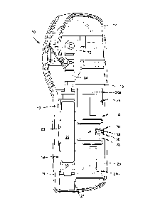
Referring now to FIG. 2, bottom section 14 of tag 10 is shown. Tag 10 can
include a
plurality of chambers to house various components. EAS component 16 is located
along
the long side of an RFID component 18. In one embodiment, EAS component 16
resides
within a first chamber (not shown) and RFID component 18 resides in a separate
chamber
(not shown). However, regardless of whether these two components are in a
separate
chamber or not, EAS component 16 and RFID component 18 maintain a side-by-side
-
relationship with each other. EAS component 16 is an EAS label or tag which
may
include, for example, but is not limited to, a magnetic resonator element (not
shown)
situated below a housing spacer 20 made of plastic or some other material,
which is
CA 02767094 2011-12-29
WO 2011/002495 PCT/US2010/001835
situated below a bias magnet 22 (or other EAS type resonant circuits). Other
EAS
elements not specifically disclosed herein may perform the function of EAS
component
16.
Alongside the EAS component 16 is RFID component 18. RFID component 18
may include, for example, a semiconductor integrated circuit 30 and a tunable
antenna.
The tunable antenna, such as antenna inlay 24 shown in FIG. 2, may be tuned to
a desired
operating frequency by adjusting the length of the antenna. The range of
operating
frequencies may vary, although the embodiments may be particularly useful for
ultra-high
frequency (UHF) spectrum. Depending upon the application and the size of the
area
available for the antenna 24, the antenna 24 may be tuned within several
hundred
Megahertz (MHz) or higher, such as 868-950 MHz, for example. In one
embodiment, for
example, the tunable antenna 24 may be tuned to operate within an RFID
operating
frequency, such as the 868 MHz band used in Europe, the 915 MHz Industrial,
Scientific
and Medical (ISM) band used in the United States, and the 950 MHz band
proposed for
Japan. It is again noted that these operating frequencies are given by way of
example
only, and the embodiments are not limited in this context.
RFID component 18 may also be a RFID security tag which includes memory to
store RFID information and which communicates the stored information in
response to an
interrogation signal transmitted by an RFID reader. RFID information may
include any
type of information capable of being stored in a memory used by RFID component
18.
Examples of RFID information include a unique tag identifier, a unique system
identifier,
an identifier for the monitored object, and so forth. The types and amount of
RFID
information are not limited in this context.
RFID component 18 may also be a passive RFID security tag. A passive RFID
security tag does not use an external power source, but rather uses the energy
in
11
CA 02767094 2011-12-29
WO 2011/002495
PCT/US2010/001835
interrogation signals as a power source. RFID component 18 may be activated by
a direct
current voltage that is developed as a result of rectifying the incoming RF
carrier signal
including interrogation signals. Once the RFID components activated, it may
then
transmit the information stored in its memory register via response signals.
In one embodiment, RFID component 18 is an RFID label or tag and includes a
hybrid antenna inlay 24 having a pair of inward spiral antennas 26a and 26b
(collectively
"26"), a magnetic loop antenna 28 situated between and in electrical contact
with spiral
antennas 26a and 26b, and an integrated circuit 30 in electrical contact with
magnetic loop
antenna 28. The hybrid antenna inlay design of the present disclosure
maintains the far
field response abilities of the spiral antenna 26 while increasing the near
field magnetic
performance due to magnetic loop antenna 28. A detailed view of the hybrid
antenna
inlay is shown in FIG. 3 and is discussed in greater detail below.
Referring again to FIG. 2, tag 10 includes an attachment clamp 32 which is
located
at the forward end of tag 10 opposite RFID component 18 and EAS component 16.
Attachment clamp 32 is typically metal and cooperates with an attachment
element, such
as a pin, to attach security tag 10 to an item to be secured (e.g. an article
of clothing).
Advantageously, attachment clamp 32 is situated at least a predetermined
distance away
from both the EAS component 16 and the RFID component and includes an extended
portion 34 to further provide a "buffer", that separates clamp 32 from EAS
component 16
and RFID component 18. The location of clamp 32 within housing 12 and the
distance it
is situated away from EAS component 16 and RFID component 18 minimizes de-
tuning of
the RFID component 18 and EAS component 16 even when clamp 32 is exposed to
large
magnetic field levels.
RFID antenna inlay 24 and housing 12 include a location key structure in order
to
ensure that the RFID integrated circuit 30 is located away from the elements
of EAS
12
CA 02767094 2011-12-29
WO 2011/002495
PCT/US2010/001835
component 16 when RFID component 18 is inserted within housing 12. In one
embodiment, the location key structure includes an aperture or a notch 36
(best seen in
FIG. 3) formed in RFID antenna inlay 24, which cooperates with a corresponding
protruding alignment flange 38 located in the interior bottom surface of
housing 12.
"Bottom surface" or "bottom interior surface" as defined herein shall mean any
surface
within the interior of bottom section 14. Thus, flange 38 might be located at
the actual
bottom interior surface of bottom section 14 or may be located along the side
walls of the
interior of bottom section 14. By placing a punched hole or notch in the RFID
component
18 at a particular location and providing a mechanical key structure in the
security tag
housing 12 and RFID antenna inlay 24, the RFID integrated circuit 30 can
advantageously
be fixed in a position within housing 12 away from the position adjacent to
the elements of
EAS component 16 which may de-tune the integrated circuit 30. The key
structure may
include other mating arrangements that situate antenna inlay 24 such that
integrated circuit
30 is positioned away from EAS component 16.
Therefore, in one embodiment, housing 12 includes a first compartment 17 and a
second compartment 19, where EAS component 16 is situated within first
compartment 17
and RFID component 18 is situated within second compartment 19. As seen in
FIG. 2,
first compartment 17 includes a first longitudinal side 21 an opposing second
longitudinal
side 23. Second compartment 19 also includes a first longitudinal side 25 and
a second
longitudinal side 21, where the first longitudinal side 21 of first
compartment 17 is the
same as the second longitudinal side 21 of the second compartment 19 since
they share a
common wall. In other embodiments, each compartment will include separate
walls to
house their corresponding components. As seen in FIG. 2, the key structure
described
above is operable to position the integrated circuit 30 such that integrated
circuit 30 is
closer to first longitudinal side 25 of second compartment 19 than it is to
the second
13
CA 02767094 2011-12-29
WO 2011/002495
PCT/US2010/001835
longitudinal side 21 of second compartment 19 when antenna inlay 24 is
inserted within
the housing 12.
Thus, when RFID component 18 is inserted within housing 12, it can only be
inserted one way, i.e., in the orientation where integrated circuit 30 is
situated away from
EAS component 16, i.e., closer to the side of antenna inlay 24 that is
furthest from EAS
element 16, due to the mating of flange 38 within notch 36. This orientation
allows the
RFID antenna inlay 24 to fit snugly within housing 12 or within a chamber in
housing 12
and upon one or more support pins (shown in FIG. 4). Trying to insert RFID
component
18 within housing 12 with RFID antenna inlay 24 facing in the opposite
direction, i.e.,
with integrated circuit 30 along side EAS component 16, would result in an
improper fit
due to flange 38 forcing RFID antenna inlay 24 upwards and out of its
alignment within
housing 12 and not allowing the top cover of housing 12 to properly mate with
bottom
section 14. Therefore, the present invention advantageously insures the proper
placement
of RFID component 18 within housing 12 situating integrated circuit away from
EAS
component 16 thus minimize potential de-tuning of integrated circuit 30 due to
the effects
of the elements of EAS component 16.
FIG. 3 illustrates one embodiment of RFID antenna inlay 24, having two inward
spiral antennas 26a and 26b, as well as a rectangular magnetic loop antenna 28
coupled to
the inward spiral antennas 26a and 26b. Although there may be a slight
frequency shift,
the insertion of RFID antenna inlay 24 within housing 12 does not affect the
relative
sensitivity of the RFID component 18 and has minimal power loss. Thus, the
design of
housing 12 and the relative positioning of EAS component 16 and RFID component
18
have relatively little effect on the overall RFID performance of tag 10.
Integrated circuit
is electrically connected to magnetic loop antenna 28 and magnetic loop
antenna 28 is
25 then electrically connected to the inward spiral antennas 26a and 26b as
shown in FIG. 3.
14
CA 02767094 2011-12-29
WO 2011/002495
PCT/US2010/001835
The overall geometry of magnetic loop antenna 28 is such that the near field
magnetic H
performance is optimized. Spiral antennas 26a and 26b dominate the far field
response.
Magnetic loop antenna 28 also acts to reduce electrostatic discharge ("ESD")
damage to integrated circuit 30 by diverting current away from the integrated
circuit 30.
For low frequency or static electric E fields produced by manufacturing
processes or
ultrasonic welding of housing 12, the magnetic loop antenna 28 is essentially
a short
circuit across integrated circuit 30. If an electrical discharge initiates
from one end of
spiral antenna 26a to the end of spiral antenna 26b, or vice versa, loop
antenna 28 diverts
the discharge current away from integrated circuit 30.
Physically, the spiral antennas 26a and 26b are connected to magnetic loop
antenna
28 and not directly to integrated circuit 30. When an E field is applied along
the length of
RFID antenna inlay 24 shown in FIG. 3, the current starts at the end of spiral
antenna 26a
(the left spiral in FIG. 3) at low levels and gradually increases to the
connection point of
the magnetic loop antenna 28. This current sense is counterclockwise. The
current
through magnetic loop antenna 28 is also of a counterclockwise sense but at
much larger
values. The current from the magnetic loop connection point to the right side
spiral
antenna 26b is of a counterclockwise sense and gradually decreases toward the
end of this
antenna trace. Thus, the direction of the currents in each spiral antenna 26a
and 26b are
the same.
RFID antenna inlay 24 shown in FIG. 3 is then placed inside of housing 12 of
the
combination EAS/RFID security tag 10, which also contains EAS component 16 and
attachment clamp mechanism 32. The EAS/RFID security tag 10 utilizing the
hybrid
antenna inlay 24 of FIG. 3 can be read by a conventional RFID reader.
An example of a near field reader magnetic H field loop antenna used with the
present invention is a 2 cm. diameter circular loop using a step-down
transformer at the
' 15
CA 02767094 2011-12-29
WO 2011/002495
PCT/US2010/001835
feed end of the loop, two tuning capacitors at the halfway point, and a
terminating resistor
at the opposite end of the loop. However, the invention is not limited to a
particular
diameter or type of near field reader magnetic loop antenna. Near field
magnetic loop
antenna 28 may also include a cylindrical slug of ferrite material.
Housing 12, which may be made of a plastic material, is configured to maintain
RFID component 18 in a.position within housing 12 so that it does not contact
the top or
bottom inside surfaces of security tag 10 in order to further minimize the
possibility of de-
tuning the RFID component 18. In one embodiment, housing 12 is configured to
position
RFID component 18 closer to the bottom surface of housing 12 than to the top
surface of
housing 12. As used herein, "bottom surface" and "bottom portion" refer to the
solid
portion of housing 12 and "top surface" and "top portion" refer to the portion
of the
housing 12 having the opening through which the locking pin is inserted for
mating with
clamp 32. By positioning RFID component 18 closer to the bottom surface of tag
10,
which faces the top surface of a tag detacher device, the near field coupling
to the detacher
antenna is improved over other arrangements.
FIGS. 4 and 5 show how tag housing 12 supports EAS component 16 and RFID
component 18 so that no separate spacer part is required for the RFID
component 18.
RFID antenna inlay 24 is located away from the top and bottom inner surfaces
of housing
12, but, in one embodiment, is closer to the bottom surface of housing 12,
which faces the
detacher. Referring specifically to FIG. 4, RFID antenna inlay 24 can be seen
within
housing 12. RFID antenna inlay 24 is supported by one or more support lower
protrusions
40. Lower protrusions 40 extend upwards from the bottom surface of housing 12
and
support RFID antenna inlay 24 which rests thereon. Lower protrusions 40 serve
to assure
that RFID antenna inlay 24 does not contact the bottom portion 44 of housing
12 in order
to further minimize the possibility of de-tuning the RFID component 18.
16
CA 02767094 2011-12-29
WO 2011/002495 PCT/US2010/001835
As is shown in FIG. 4, in addition to being supported by lower protrusions 40,
RFID antenna inlay 24 is also positioned beneath upper protrusions 42. Upper
protrusions
42 serve to position RFID antenna inlay 24 away from the upper portion 46 of
housing 12
to minimize the possibility of de-tuning the RFID component 18 and to secure
RFID
antenna inlay 24 within housing 12. In this embodiment, upper protrusions 42
are longer
than lower protrusions 40, which results in RFID antenna inlay 24 being
positioned closer
to the lower part of housing 12, i.e., closer to the bottom portion 44 of
housing 12 than the
top portion 46 of housing 40. As discussed above, this advantageously
positions RFID
component 18 closer to the tag detacher's top surface when the tag detacher is
used to
remove the article from the tag 10.
FIG. 5, like FIG. 4, shows a section view of the housing 12 of tag 10. While
FIG.
4 showed the RFID component 18, i.e., RFID antenna inlay 24, FIG. 5
illustrates the EAS
component 16 of tag 10. The elements of EAS component 16, magnetic resonator
element
15, spacer 20 and bias magnet 22, can be seen. These components are not
supported by
lower projections 40. Lower projections 40 only support RFID component 18 and,
in one
embodiment, lower projections 40 are situated only in second compartment 19
that houses
RFID antenna inlay 24. From the view shown in FIG. 5, RFID antenna inlay 24
cannot
be seen. However, RFID antenna inlay 24, supported by lower protrusions 42,
resides in
housing 12 such that it is substantially co-planar with bias magnet 22 and
situated above
magnetic resonator element 15. This arrangement provides minimizes the loading
effect
on the RFID signal and provides tag 10 with optimal read performance.
FIG. 6 illustrates a cut-away illustration of housing 12, viewed from the end
of tag
10 looking towards the top of tag 10. In this view, the planar relationship
between RFID
component 18 and EAS component 16 can readily be seen. EAS component 16
includes
magnetic resonator element 15, upon which is situated spacer 20, upon which is
situated
17
CA 02767094 2011-12-29
WO 2011/002495 PCT/US2010/001835
bias magnet 22. Bias magnet 22 is situated within housing 12 such that it is
at
substantially the same height as antenna inlay 24 of RFID component 18.
Antenna inlay
24 is situated within housing 12 such that it is higher, i.e., closer to the
top surface of
housing 12, than spacer 20 and higher than magnetic resonator element 15.
FIG. 7 represents a graph illustrating a comparison of the read power
sensitivity for
RFID antenna inlay 24 tuned, for example, for 868 MHz, both inside the housing
12 of tag
10, represented by graph 48, and outside of tag 10, represented by graph 50.
Although the
frequency is shifted, the power sensitivity remains about the same. Thus, the
housing 12
and other components of tag 10 such as EAS element 16, does not impact the
power
sensitivity from RFID antenna inlay 24.
While certain features of the embodiments have been illustrated as described
herein, many modifications, substitutions, changes and equivalents will now
occur to those
skilled in the art. It is therefore to be understood that the appended claims
are intended to
cover all such modifications and changes as fall within the true spirit of the
embodiments.
It will be appreciated by persons skilled in the art that the present
invention is not
limited to what has been particularly shown and described herein above. In
addition,
unless mention was made above to the contrary, it should be noted that all of
the
accompanying drawings are not to scale. A variety of modifications and
variations are
possible in light of the above teachings without departing from the scope and
spirit of the
invention, which is limited only by the following claims.
In addition, unless mention was made above to the contrary, it should be noted
that
all of the accompanying drawings are not to scale. Significantly, this
invention can be
embodied in other specific forms without departing from the spirit or
essential attributes
thereof, and accordingly, reference should be had to the following claims,
rather than to
the foregoing specification, as indicating the scope of the invention.
18