Note : Les descriptions sont présentées dans la langue officielle dans laquelle elles ont été soumises.
CA 02767628 2012-01-09
WO 2011/005941 PCT/US2010/041341
PATENT
Attorney Docket No.: EE028PCT
METHOD AND APPARATUS FOR SINGLE-PATH CONTROL AND MONITORING
OF AN H-BRIDGE
BACKGROUND OF THE INVENTION
Field of the Invention
[0001] Embodiments of the present disclosure generally relate to power
conversion and, more particularly, to a method and apparatus for monitoring
and
controlling DC/AC power conversion.
Description of the Related Art
[0002] A common topology for a DC/AC power conversion module (i.e., a DC/AC
inverter) is to employ a DC/DC booster stage followed by an H-bridge. The
DC/DC
booster stage generates a rectified sine-wave output and the H-bridge,
operating at
the frequency of an AC line coupled to the output of the DC/AC inverter,
creates a
true AC waveform by "unfurling" the rectified sine-wave from the DC/DC booster
stage. In some instances, the AC output from the DC/AC inverter may be coupled
to
a commercial AC power line. For example, solar power generation systems
utilizing
DC/AC inverters convert DC power produced by photovoltaic modules to AC power
that may be coupled to the commercial AC power grid.
[0003] In order to generate the required AC waveform output, the DC/AC
inverter
generally receives control signals from a controller via a control signal path
for
operating the H-bridge, i.e., for alternately switching the diagonals of the H-
bridge on
and off. Additionally, the DC/AC inverter generally provides one or more
monitoring
signals back to the controller via a monitoring signal path. The monitoring
signals
indicate any fault occurrences in the H-bridge and trigger the controller to
shut-down
the DC/DC booster stage and the H-bridge to prevent any damage in such a
situation. Such control and monitoring signal paths require additional
components
and connections within the power conversion module and consume additional
space
within the power conversion module.
1
CA 02767628 2012-01-09
WO 2011/005941 PCT/US2010/041341
PATENT
Attorney Docket No.: EE028PCT
[0004] Therefore, there is a need for a method and apparatus for providing
control signals to an H-bridge and receiving monitoring signals from the H-
bridge
utilizing a single communication path.
SUMMARY OF THE INVENTION
[0005] Embodiments of the present invention generally relate to a method and
apparatus for controlling and monitoring an H-bridge via a single
communication
path. The apparatus comprises a first control and monitor module coupled to a
first
switch within the H-bridge; and a first pulse transformer coupled to a first
control
signal to the first control and monitor module, wherein the first control and
monitor
module (i) generates, based on the first control signal, a first driver signal
for
operating a first switch of the H-bridge during DC/AC power conversion, (ii)
monitors
at least a portion of the H-bridge for at least one fault, and (iii)
communicates, upon
detecting the at least one fault, a first fault indication to a main
controller of the H-
bridge via the first pulse transformer.
BRIEF DESCRIPTION OF THE DRAWINGS
[0006] So that the manner in which the above recited features of the present
invention can be understood in detail, a more particular description of the
invention,
briefly summarized above, may be had by reference to embodiments, some of
which
are illustrated in the appended drawings. It is to be noted, however, that the
appended drawings illustrate only typical embodiments of this invention and
are
therefore not to be considered limiting of its scope, for the invention may
admit to
other equally effective embodiments.
[0007] Figure 1 is a block diagram of a power conversion module in accordance
with one or more embodiments of the present invention;
[0008] Figure 2 is a schematic diagram of a DC/AC inversion stage in
accordance with one or more embodiments of the present invention;
[0009] Figure 3 is a schematic diagram of a control and monitor module in
accordance with one or more embodiments of the present invention;
139699-1 2
CA 02767628 2012-01-09
WO 2011/005941 PCT/US2010/041341
PATENT
Attorney Docket No.: EE028PCT
[0010] Figure 4 is a schematic diagram of a switch controller in accordance
with
one or more embodiments of the present invention;
[0011] Figure 5 is a plurality of waveforms depicting DC/AC inversion stage
control and monitoring signals in accordance with one or more embodiments of
the
present invention;
[0012] Figure 6 is a flow diagram of a method for controlling and monitoring
an H-
bridge in accordance with one or more embodiments of the present invention;
and
[0013] Figure 7 is a schematic diagram of a control and monitor module coupled
to a single winding secondary coil in accordance with one or more embodiments
of
the present invention.
DETAILED DESCRIPTION
[0014] Figure 1 is a block diagram of a power conversion module 100 in
accordance with one or more embodiments of the present invention. The power
conversion module 100 receives DC input power from a DC source and produces
AC output power. In some embodiments, the power conversion module 100
receives the DC input power from one or more solar powered photovoltaic (PV)
module(s); alternatively, the power conversion module 100 may receive the DC
input
power from any suitable DC power source. The power module 100 converts the
DC power into AC power that may be coupled to a commercial AC power grid
("power grid"), coupled to one or more appliances, and/or stored for later use
(e.g.,
utilizing batteries, heated water, hydro pumping, H2O-to-hydrogen conversion,
or the
like).
[0015] The power conversion module 100 comprises a DC/DC booster 102, a
DC/AC inversion stage 104, a main controller 106, and an AC voltage sampler
108.
The DC/DC booster 102 is coupled via two input terminals to the DC power
source
and via two output terminals to the DC/AC inversion stage 104; the DC/DC
booster
102 is further coupled to the main controller 106. The DC/DC booster 102
converts
the DC input power to a DC output power (i.e., a rectified sine wave output)
in
139699-1 3
CA 02767628 2012-01-09
WO 2011/005941 PCT/US2010/041341
PATENT
Attorney Docket No.: EE028PCT
accordance with DC/DC conversion control signals received from the main
controller
106. The output power from the DC/DC booster 102 is coupled to the DC/AC
inversion stage 104.
[0016] The DC/AC inversion stage 104 is coupled to the main controller 106 and
converts the DC power from the DC/DC booster 102 to AC power in accordance
with DC/AC conversion control signals received from the main controller 106.
The
AC power from the DC/AC inversion stage 104 is coupled to an AC line, for
example, the power grid. The AC voltage sampler 108 is coupled to the two
output
terminals of the DC/AC inversion stage 104 and to the main controller 106. The
AC
voltage sampler 108 provides samples of the AC line voltage to the main
controller
106 for generating the power conversion control signals.
[0017] In accordance with one or more embodiments of the present invention,
the
main controller 106 provides control signals to the DC/AC inversion stage 104
and
receives monitoring signals from the DC/AC inversion stage 104 via a single
communication path, as described in detail below.
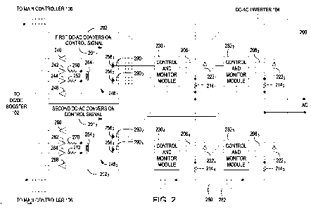
[0018] Figure 2 is a schematic diagram of a DC/AC inversion stage 104 in
accordance with one or more embodiments of the present invention. The DC/AC
inversion stage 104 comprises coupler modules 202, and 2022 (collectively
referred
to as coupler modules 202), n-type MOSFET switches 2061, 2062, 2063, and 2064
(collectively referred to as switches 206), resistors 2141, 2142, 2143, and
2144
(collectively referred to as resistors 214), diodes 2221, 2222, 2223, and
2224,
(collectively referred to as diodes 222), and control and monitor modules
2301, 2302,
2303, and 2304 (collectively referred to as control and monitor modules 230).
In
alternative embodiments, one or more of the switches 206 may be an insulated
gate
bipolar transistor (IGBT), a gate turn-off (GTO) switch, a bipolar junction
transistor
(BJT), or the like, or some combination thereof.
[0019] The coupler modules 202, and 2022 operate to couple control signals
from
the main controller 106 to the control and monitor modules 230 and also to
couple
fault indications from the control and monitor modules 230 to the main
controller
139699-1 4
CA 02767628 2012-01-09
WO 2011/005941 PCT/US2010/041341
PATENT
Attorney Docket No.: EE028PCT
106. The coupler module 202, comprises a pulse transformer 248, and buffers
240,
242, 244, and 246. The pulse transformer 248, comprises a primary winding 254,
and two identical secondary windings, 256, and 2563, where each secondary
winding 256, and 2563 comprises a tap 290, and 2903, respectively. An output
terminal of the buffer 242 is coupled to a first terminal of a resistor 250; a
second
terminal of the resistor 250 is coupled to an input terminal of the buffer 240
and a
first terminal of the primary winding 2541. An output terminal of the buffer
244 is
coupled to a first terminal of a resistor 252; a second terminal of the
resistor 252 is
coupled to an input terminal of the buffer 246 and to a second terminal of the
primary winding 2541. Output terminals of the buffers 240 and 246 and input
terminals of the buffers 242 and 244 are coupled to the main controller 106.
The
secondary windings 256, and 2563, including their respective taps 290, and
2903,
are coupled to control and monitor modules 230, and 2303, respectively.
[0020] The coupler module 2022 comprises a pulse transformer 2482 and buffers
260, 262, 264, and 266. The pulse transformer 2482 comprises a primary winding
2542 and two identical secondary windings, 2562 and 2564, where each secondary
winding 2562 and 2564 comprises a tap 2902 and 2904, respectively. An output
terminal of the buffer 262 is coupled to a first terminal of a resistor 270; a
second
terminal of the resistor 270 is coupled to an input terminal of the buffer 260
and a
first terminal of a primary winding 2542. An output terminal of the buffer 264
is
coupled to a first terminal of a resistor 272; a second terminal of the
resistor 272 is
coupled to an input terminal of the buffer 266 and to a second terminal of the
primary winding 2542. Output terminals of the buffers 260 and 266 and input
terminals of the buffers 262 and 264 are coupled to the main controller 106.
The
secondary windings 2562 and 2564, including their respective taps 2902 and
2904,
are coupled to control and monitor modules 2302 and 2304, respectively. In
some
alternative embodiments, the secondary windings 256 may each be a single
winding
transformer rather than a tapped transformer, as described below with respect
to
Figure 7.
139699-1 5
CA 02767628 2012-01-09
WO 2011/005941 PCT/US2010/041341
PATENT
Attorney Docket No.: EE028PCT
[0021] The switches 206 are coupled in an H-bridge configuration with switches
206, and 2063 forming a first diagonal of the H-bridge and switches 2062 and
2064
forming a second diagonal of the H-bridge. A drain terminal of the switch 206,
is
coupled to a first output terminal of the DC/DC booster 102, and a source
terminal of
the switch 206, is coupled to a first terminal of the resistor 2141. A second
terminal
of the resistor 214, is coupled to a first output terminal of the DC/AC
inversion stage
104 and to a drain terminal of the switch 2064. A source terminal of the
switch 2064
is coupled to a first terminal of the resistor 2144, and a second terminal of
the
resistor 2144 is coupled to a second output terminal of DC/DC booster 102.
[0022] A drain terminal of the switch 2062 is coupled to the first output
terminal of
the DC/DC booster 102, and a source terminal of the switch 2062 is coupled to
a first
terminal of the resistor 2142. A second terminal of the resistor 2142 is
coupled to a
second output terminal of the DC/AC inversion stage 104 and to a drain
terminal of
the switch 2063. A source terminal of the switch 2063 is coupled to a first
terminal of
the resistor 2143, and a second terminal of the resistor 2143 is coupled to
the second
output terminal of DC/DC booster 102.
[0023] The diodes 2221, 2222, 2223, and 2224 are each coupled across the
switches 2061, 2062, 2063, and 2064, respectively, such that each diode anode
terminal is coupled to the corresponding switch source terminal and each diode
cathode terminal is coupled to the corresponding switch drain terminal; in
some
embodiments, the diodes 222 are an integral part of the switches 206.
[0024] The control and monitor modules 230 are coupled to the H-bridge for
controlling the operation of the H-bridge (i.e., activating and deactivating
the
switches 206) and monitoring the H-bridge for fault conditions. In the event
of a
detected fault condition, the control and monitor modules 230 drive the H-
bridge to
shut-down such that no current passes through any of the H-bridge switches. In
some embodiments, the control and monitor modules 230 are low-voltage
integrated
circuits (ICs).
139699-1 6
CA 02767628 2012-01-09
WO 2011/005941 PCT/US2010/041341
PATENT
Attorney Docket No.: EE028PCT
[0025] The control and monitor modules 2301, 2302, 2303, and 2304 are coupled
in a one-to-one correspondence to the gate and source terminals of the
switches
2061, 2062, 2063, and 2064, respectively. Additionally, the control and
monitor
modules 2301, 2302, 2303, and 2304 are coupled in a one-to-one correspondence
to
the second terminals of the resistors 2141, 2142, 2143, and 2144,
respectively. The
control and monitor modules 2301, 2302, 2303, and 2304 are coupled to the
secondary windings 2561, 2562, 2563, and 2564, respectively, for receiving
control
signals from the main controller 106 and providing fault indications to the
main
controller 106. Additionally, the control and monitor modules 2303, and 2304
are
coupled together via two lines (i.e., lines 280 and 282) for communicating
detected
fault conditions to one another.
[0026] During normal operating conditions (i.e., no fault conditions), the
control
and monitor modules 230 drive the switches 206 in accordance with DC/AC
conversion control signals 202 from the main controller 106. During such
operation,
the diagonal switch pairs 2061/2063 and 2062/2064 are sequentially activated
and
deactivated to convert DC power from the DC/DC booster 102 to AC power at the
output of the DC/AC inversion stage 104. The diagonal switch pairs 2061/2063
and
2062/2064 each conducts current for half of an AC line voltage cycle and
operate in a
mutually exclusive fashion; i.e., each diagonal switch pair is on or off
during the
opposite half-cycle from the other diagonal switch pair. In some embodiments,
the
resulting AC power from the DC/AC inversion stage 104 is synchronously coupled
to
the commercial power grid. In some alternative embodiments, the switches 206
may be driven at higher frequencies (e.g., tens of kilohertz and higher) for
alternative
applications, such as for a DC/DC converter.
[0027] In order to drive the sequential switching of the diagonal switch
pairs, the
main controller 106 applies a first DC/AC conversion control signal 201, via
the
pulse transformer 2481 to the control and monitor modules 2301 and 2303 and a
second DC/AC conversion control signal 2012 via the pulse transformer 2482 to
the
control and monitor modules 2302 and 2304. The control and monitor modules 230
drive the corresponding switches 206 in accordance with the DC/AC conversion
139699-1 7
CA 02767628 2012-01-09
WO 2011/005941 PCT/US2010/041341
PATENT
Attorney Docket No.: EE028PCT
control signals 201. In some embodiments, the secondary windings 256 may be
such that the magnitude of the DC/AC conversion control signal 201 is stepped-
up
on the secondary side of the pulse transformer; for example, a step-up may be
required to increase from 3.3V logic to 10V for operating a MOSFET switch. In
some alternative embodiments, the secondary windings 256 may be such that no
change in voltage level occurs or the voltage level is stepped-down on the
secondary side of the pulse transformer 248.
[0028] The first and second DC/AC conversion control signals 2011, 2012
comprise high-frequency (e.g., on the order of megahertz) periodic dual-
polarity
pulses that drive the operation of the switches 206 in accordance with their
duty
cycle. By operating at such high frequencies (e.g., at frequencies much higher
than
the frequency of the power grid), relatively small and cost effective pulse
transformers 248 may be utilized. In some embodiments, the DC/AC conversion
control signals 201 drive the corresponding control and monitor modules 230 to
turn
on the subtending switches 206 when the DC/AC conversion control signal duty
cycle is greater than 50% and to turn off the subtending switches 206 when the
DC/AC conversion control signal duty cycle is less than 50%. For example, the
DC/AC conversion control signals 201, and 2012 may each comprise a periodic
series of pulses having a 75% duty cycle ("three-quarters pulse") and a
periodic
series of pulses having a 25% duty cycle ("one-quarter pulse"), where the
three-
quarters pulse signal drives the corresponding downstream switches 206 in an
on-
state and the one-quarter pulse signal drives the corresponding downstream
switches 206 in an off-state. One embodiment of a DC/AC conversion control
signal
201 is described below with respect to Figure 5.
[0029] In addition to controlling the H-bridge functionality during normal
operating
conditions, the control and monitor modules 230 monitor for one or more fault
conditions, such as excessive current flowing through the switches 206 (i.e.,
overcurrent), large negative current flowing through the switches 206, under-
voltage
lockout (UVLO) (i.e., insufficient power for operating the control and monitor
module
230), over-temperature faults, or the like. When a fault condition is detected
by a
139699-1 8
CA 02767628 2012-01-09
WO 2011/005941 PCT/US2010/041341
PATENT
Attorney Docket No.: EE028PCT
control and monitor module 230, the control and monitor module 230 deactivates
its
subtending switch 206 and may trigger one or more of the remaining control and
monitor modules 230 to deactivate their corresponding switch 206.
Additionally, the
control and monitor module 230 detecting the fault provides a fault indicator
signal
back to the main controller 106 via the corresponding secondary winding 256;
i.e.,
the fault indicator signal from the control and monitor module 230 to the main
controller 106 utilizes the same communication path as the control signals
from the
main controller 106 to the control and monitor module 230. The fault indicator
signal
triggers the main controller 106 to deactivate all of the switches 206.
[0030] Figure 3 is a schematic diagram of a control and monitor module 230 in
accordance with one or more embodiments of the present invention. The control
and monitor module 230 comprises diodes 302, 304, 306, and 308; an input
capacitor 310; a MOSFET monitor switch 312; and a switch controller 314. In
some
alternative embodiments, the monitor switch 312 may be a switch such as an
insulated gate bipolar transistor (IGBT), a gate turn-off (GTO) switch, a BJT,
or the
like, or some combination thereof.
[0031] Anode terminals of the diodes 302 and 304 are coupled to a first
terminal
of the secondary winding 256 of coupler module 202, and anode terminals of the
diodes 306 and 308 are coupled to a second terminal of the secondary winding
256.
Cathode terminals of the diodes 304 and 308 are coupled to a first terminal of
the
input capacitor 310 and to a power input terminal 322 of the switch controller
314 for
providing power to the switch controller 314; in some embodiments, the switch
controller 314 may be on the order of a 10 volt or 15 volt integrated circuit
(IC).
Cathode terminals of the diodes 302 and 306 are coupled to a drain terminal of
the
monitor switch 312 and to an H-bridge control input terminal 324 of the switch
controller 314 for providing an H-bridge control signal 316 to the switch
controller
314. A second terminal of the input capacitor 310, a source terminal of the
monitor
switch 312, and the switch controller 314 are further coupled to the tap 290
of the
secondary winding 256 and to the second terminal of the resistor 214. The
switch
controller 314 is further coupled to the first terminal of the resistor 214,
the gate
139699-1 9
CA 02767628 2012-01-09
WO 2011/005941 PCT/US2010/041341
PATENT
Attorney Docket No.: EE028PCT
terminal of the switch 206, and the gate terminal of the monitor switch 312.
Additionally, the switch controller 314 of the control and monitor module 2303
is
coupled to a switch controller 314 of the control and monitor module 2304-
[0032] The secondary winding 256 provides an input signal to the control and
monitor module 230 based on the DC/AC conversion control signal 201 supplied
by
the main controller 106 to the primary winding 254. The diodes 304 and 308
rectify
the DC/AC input signal received from the secondary winding 256 and couple the
resulting power control signal 326 to the input capacitor 310 and to the power
input
terminal 322. When the power control signal 326 has a high value, the power
control signal 326 provides power to the switch controller 314 and provides a
positive voltage across the input capacitor 310 (i.e., each pulse of the power
control
signal 326 provides a positive voltage across the first and second terminals
of the
input capacitor 310). When the power control signal 326 has a low value, the
input
capacitor 310 discharges to provide power to the switch controller 314. Thus,
the
diodes 304, 308 and the capacitor 310 form a DC power source for the switch
controller 314.
[0033] The diodes 302 and 306 rectify the input signal received from the
secondary winding 256 and couple the resulting H-bridge control signal 316 to
the
H-bridge control input terminal 324 and to the drain terminal of the monitor
switch
312; one embodiment of the H-bridge control signal 316 is described below with
respect to Figure 5. During normal operating conditions (i.e., no fault
conditions),
the switch controller 314 generates an H-bridge driver signal 318 that drives
the
switch 206 in accordance with the duty cycle of the H-bridge control signal
316; for
example, the switch 206 is activated when the H-bridge control signal duty
cycle is
greater than 50% and deactivated when the H-bridge control signal duty cycle
is less
than 50%. Additionally during normal operating conditions, the switch
controller 314
generates a monitor switch driver signal 320 for maintaining the monitor
switch 312
in an off-state.
[0034] The switch controller 314 monitors for one or more fault conditions,
such
as excessive current flowing through the switch 206 (i.e., overcurrent), large
139699-1 10
CA 02767628 2012-01-09
WO 2011/005941 PCT/US2010/041341
PATENT
Attorney Docket No.: EE028PCT
negative current flowing through the switch 206, under-voltage lockout (UVLO),
over-temperature faults, or the like. When a fault condition is detected by
the switch
controller 314, the switch controller 314 generates an H-bridge driver signal
318 that
deactivates the switch 206, prohibiting current flow through the switch 206.
Additionally, the switch controller 314 generates a monitor switch driver
signal 320
such that the monitor switch 312 is alternately activated and deactivated
based on
the H-bridge control signal 316. In some embodiments, the monitor switch
driver
signal 320 activates the monitor switch 312 after 25% of the period of the H-
bridge
control signal 316 and deactivates the monitor switch 312 at the end of each
period
of the H-bridge control signal 316. Such operation of the monitor switch 312
periodically shorts the H-bridge control input terminal 324, thereby
"clamping" the
switch control signal 316 and the DC/AC conversion control signal 201 at a 25%
duty cycle. Such clamping of the switch control signal 316 and the DC/AC
conversion control signal 201 provides a fault indicator signal back to the
main
controller 106 via the pulse transformer 248 and additionally causes the
control and
monitor module 230 sharing the same pulse transformer 248 to deactivate its
corresponding H-bridge switch 206.
[0035] Additionally, when a fault condition is detected the switch controller
314
may couple a "fault out" signal via line 280 to switch controller 314 within a
second
control and monitor module 230, causing the second control and monitor module
230 to deactivate its subtending switch 206. The switch controller 314 may
additionally or alternatively receive a "fault in" signal from the second
control and
monitor module 230 via line 282, indicating that the second control and
monitor
module 230 has identified a fault condition and causing the switch controller
314 to
turn off its subtending switch 206.
[0036] Figure 4 is a schematic diagram of a switch controller 314 in
accordance
with one or more embodiments of the present invention. The switch controller
314
comprises a blanking module 402 and an input decision module 404, each coupled
to the H-bridge control input terminal 324for receiving the H-bridge control
signal
316. The input decision module 404 is further coupled to a first input of a
logical
139699-1 11
CA 02767628 2012-01-09
WO 2011/005941 PCT/US2010/041341
PATENT
Attorney Docket No.: EE028PCT
AND gate 406, and the AND gate 406 receives a second input from a logical NOR
gate 408. The AND gate 406 generates the H-bridge driver signal 318 and
couples
such signal to the gate terminal of the switch 206 for driving the switch 206.
[0037] The switch controller 314 further comprises reference voltages 426 and
428, each coupled to the second terminal of the resistor 214. The reference
voltages 426 and 428 are further coupled to an inverting input of a comparator
420
and a non-inverting input of a comparator 422, respectively. A non-inverting
input of
the comparator 420 and an inverting input of the comparator 422 are coupled to
the
source terminal of switch 206. Outputs from the comparators 420 and 422 are
coupled to a first and a second input of a logical OR gate 418, respectively,
and an
output from the OR gate 418 is coupled to an input of a fault indicator 412.
In some
embodiments, the fault indicator 412 comprises a monostable circuit or similar
circuitry that generates a high signal output in response to receiving a high
signal
input.
[0038] An output of the fault indicator 412 is coupled to a first input of a
logical
OR gate 410, and an output of the OR gate 410 is coupled to an input of the
NOR
gate 408. In some embodiments, one or more additional fault indicator
circuits, such
as under-voltage lockout (UVLO) fault indicator 414 and/or over-temperature
fault
indicator 416, may be coupled to additional inputs of the OR gate 410. In such
embodiments, the UVLO fault indicator 414 indicates a fault (e.g., by
generating a
high output) when the voltage across the capacitor 310/switch controller 314
is
insufficient for proper operation. The over-temperature fault indicator 416
indicates
a fault (e.g., by generating a high output) when the controller temperature or
the
switch temperature satisfies a threshold; for example, a temperature sensor
may be
co-located with the switch 312 within the control and monitor module 230 for
indicating the switch temperature. In some alternative embodiments, the OR
gate
410 is omitted from the switch controller 314 and the output from the fault
indicator
412 is coupled to the input of the NOR gate 408. The output of the OR gate 410
is
further coupled to the blanking module 402 for driving the blanking module
402.
139699-1 12
CA 02767628 2012-01-09
WO 2011/005941 PCT/US2010/041341
PATENT
Attorney Docket No.: EE028PCT
[0039] The blanking module 402 generates the monitor switch driver signal 320
based on the received H-bridge switch signal 316 and the signal from the OR
gate
410; the blanking module 402 then couples the monitor switch driver signal 320
to
the gate terminal of the monitor switch 312 for driving the monitor switch
312. When
receiving a low-signal from the OR gate 410, the blanking module 402 generates
the
monitor switch driver signal 320 as a low-signal that deactivates the monitor
switch
312, leaving the received H-bridge control signal 316 unaltered. When
receiving a
high signal from the OR gate 410, the blanking module 402 "blanks-out" a
portion of
the duty cycle of the H-bridge control signal 316 by generating a monitor
switch
driver signal 320 that activates the monitor switch 312 after a portion of the
H-bridge
control signal period and deactivates the monitor switch 312at the end of each
H-
bridge control signal period. In some embodiments, the monitor switch 312 is
activated after 25% of the period of the H-bridge control signal 316.
[0040] In addition to controlling the blanking module 402, the output from the
OR
gate 410 provides an indication of a detected fault to the first input of the
NOR gate
408. In some embodiments, the output from the OR gate 410 may be further
coupled via line 280 to a second switch controller 314 for indicating a
detected fault
("fault out"). Additionally or alternatively, a second input to the NOR gate
408 may
be coupled via line 282 to a second switch controller 314 for receiving an
indication
of a fault detected by the second switch controller 314 ("fault in"). In some
alternative
embodiments, the second input to the NOR gate 408 may be tied to a logic zero,
or
the NOR gate 408 may be omitted and an inverted output from the OR gate 410
coupled to the AND gate 406.
[0041] The input decision module 404 generates an output signal based on the
received H-bridge control signal 316. In some embodiments, the input decision
module 404 generates the output signal based on the duty cycle of the H-bridge
control signal 316 at a given time; for example, the input decision module 404
may
generate a high signal output when the switch control signal duty cycle is
greater
than 50% and a low-signal output when the H-bridge control signal duty cycle
is less
than 50%. The input decision module 404 may comprise a monostable circuit for
139699-1 13
CA 02767628 2012-01-09
WO 2011/005941 PCT/US2010/041341
PATENT
Attorney Docket No.: EE028PCT
providing such output signals; alternatively, a phase locked loop may be
utilized, the
signal may be averaged over one period and the averaged value compared to one-
half of the supply voltage, or a similar technique may be utilized.
[0042] During normal operating conditions (i.e. no fault conditions), all
inputs to
the OR gate 410 are low, as well as the fault in signal on line 282. The
output from
the NOR gate 408 is thus a high signal to the AND gate 406, and the output
from the
AND gate 406 (i.e., the H-bridge driver signal 318) is determined based on the
signal from the input decision module 404. When the input decision module 404
generates a high signal, the H-bridge driver signal 318 is high and the switch
206 is
activated; when the input decision module 404 generates a low-signal, the H-
bridge
driver signal 318 is low and the switch 206 is deactivated. Also during normal
operating conditions, the OR gate 410 provides a low-signal to the blanking
module
402, causing the blanking module 402 to generate the monitor switch driver
signal
320 as a low-signal for maintaining the monitor switch 312 in an off-state.
[0043] In the event of a fault condition, such as an overcurrent fault, a
negative
current fault, a UVLO fault, or an over-temperature fault, the OR gate 410
receives a
high signal from the fault indicator 412, the UVLO fault indicator 414, or the
over
temperature fault indicator 416. In the event of excessive current through the
switch
206, i.e. an over-current fault, the comparator 420 provides a high signal to
the OR
gate 418, causing the fault indicator 412 to couple a high signal to the OR
gate 410.
A threshold for determining the overcurrent fault can be set by adjusting the
reference voltage 426. In the event of a large negative current through the
switch
206, the comparator 422 provides a high signal to the OR gate 418, causing the
fault
indicator 412 to couple a high signal to the OR gate 410. A threshold for
determining the negative current fault can be set by adjusting the reference
voltage
428. In the event of a UVLO fault, the UVLO fault indicator 414 detects the
fault and
couples a high signal to the OR gate 410, and in the event of an over-
temperature
fault, the over-temperature fault indicator 416 detects the fault and couples
a high
signal to the OR gate 410.
139699-1 14
CA 02767628 2012-01-09
WO 2011/005941 PCT/US2010/041341
PATENT
Attorney Docket No.: EE028PCT
[0044] In response to the received high signal, the OR gate 410 couples a high
signal to the NOR gate 408, which in turn couples a low-signal to the AND gate
406.
Additionally or alternatively, the NOR gate may receive a high signal input
via the
line 282, resulting in a low-signal to the AND gate 406. Upon receiving the
low-
signal, the AND gate 406 generates a low H-bridge driver signal 318 that
deactivates the switch 206.
[0045] In addition to coupling the high signal to the NOR gate 408 during a
detected fault condition, the OR gate 410 couples the high signal to the
blanking
module 402. Upon receiving a high signal from the OR gate 410, the blanking
module 402 generates a periodic monitor switch driver signal 320 that becomes
high
after a first portion of the period of the H-bridge control signal 316 (i.e.,
the monitor
switch 312 is activated) and becomes low at the end of the H-bridge control
signal
period (i.e., the monitor switch 312 is deactivated). Such
activation/deactivation of
the monitor switch 312 "blanks-out" the duty cycle of the H-bridge control
signal 316
and the DC/AC conversion control signal 201 after the first portion; in some
embodiments, the monitor switch 312 is turned on after 25% of the period of
the H-
bridge control signal 316. Such blanking of the H-bridge control signal 316
and the
DC/AC conversion control signal 201 provides an indication of the detected
fault to
the main controller 106 via the pulse transformer 248, thereby communicating
the
detected fault to the main controller 106 via the same communication path
utilized to
communicate the DC/AC conversion control signal 201 for operating the H-bridge
during the DC/AC power conversion.
[0046] Figure 5 is a plurality of waveforms 500 depicting DC/AC inversion
stage
control and monitoring signals in accordance with one or more embodiments of
the
present invention. The waveforms 500 comprise a DC/AC conversion control
signal
201, an H-bridge control signal 316, an H-bridge driver signal 318, and a
monitor
switch driver signal 320.
[0047] From time To to T1, during a period of normal operating conditions
(i.e., no
faults detected), the DC/AC conversion control signal 201 comprises a series
of
periodic dual-polarity pulses having a 25% duty cycle; in other embodiments,
the
139699-1 15
CA 02767628 2012-01-09
WO 2011/005941 PCT/US2010/041341
PATENT
Attorney Docket No.: EE028PCT
DC/AC conversion control signal 201 may have a different duty cycle. The DC/AC
conversion control signal 201 is generally a high-frequency signal, for
example on
the order of megahertz. The dual-polarity DC/AC conversion control signal
pulses
are rectified by the diodes 302 and 306, as described above with respect to
Figure
3, to generate the H-bridge control signal 316.
[0048] In accordance with the duty cycle of the H-bridge control signal 316,
the
input decision module 404 generates a low H-bridge driver signal 318 and the
switch
206 is deactivated. Additionally, as a result of no detected faults, the
blanking
module 402 generates a low monitor switch driver signal 320 and the monitor
switch
312 is deactivated.
[0049] At time T1, the DC/AC conversion control signal 201 becomes a series of
periodic dual-polarity pulses having a larger duty cycle than the previous
DC/AC
conversion control signal pulses, such as a 75% duty cycle, resulting in an H-
bridge
control signal 316 that also has a larger duty cycle than the previous H-
bridge
control signal pulses (i.e., the H-bridge control signal duty cycle is the
same as the
DC/AC conversion control signal duty cycle). The H-bridge driver signal 318
and the
monitor switch driver signal 320 remain low.
[0050] At time T2, the input decision module 404 has determined that the duty
cycle of the H-bridge control signal 316 is sufficient to activate the switch
206.
Accordingly, the input decision module 404 generates a high output signal,
resulting
in a high H-bridge driver signal 318 that activates the switch 206. In some
embodiments, the input decision module 404 may generate the output signal when
the switch control signal 316 has reached 50% of its period; in other
embodiments,
the input decision module 404 may generate the output signal before or after
50% of
the switch control signal period. The blanking module 402 continues to
generate a
low monitor switch driver signal 320 and the monitor switch 312 remains
deactivated.
[0051] At time T3, while the switch 206 is activated, a fault condition is
detected.
Such a fault condition may be one or more of, for example, an overcurrent
through
139699-1 16
CA 02767628 2012-01-09
WO 2011/005941 PCT/US2010/041341
PATENT
Attorney Docket No.: EE028PCT
the switch 206, a negative current through the switch 206, an under-voltage
lockout
(UVLO) fault, or an over-temperature fault. As a result of the detected fault,
the OR
gate 410 couples a high signal to the NOR gate 408; additionally or
alternatively, the
NOR gate 408 may received a "fault in" signal from another switch controller
314.
The high input or inputs to the NOR gate 408 causes the NOR gate 408 to couple
a
low signal to the AND gate 406, resulting in a low H-bridge driver signal 318
that
deactivates the switch 206. Upon deactivation, current flow through the switch
206
ceases, thereby preventing any damage to the switch 206 from the detected
fault.
[0052] The monitor switch driver signal 320 remains low at time T3. The high
output from the OR gate 410 is coupled to the blanking module 402 and is
further
coupled as a "fault out" signal to a second switch controller 314.
[0053] The high output from the OR gate 410 causes the blanking module 402 to
generate a monitor switch driver signal 320 that becomes high at T4 (i.e., at
one
quarter of the period of the H-bridge control signal 316), activating the
monitor
switch 312 and shorting the H-bridge control signal 316. The DC/AC conversion
control signal 201 and the H-bridge control signal 316 become low (i.e., the
signals
are clamped). The H-bridge driver signal 318 remains low. In other
embodiments,
the blanking module 402 may generate a monitor switch driver signal 320 that
becomes high at a different point in the H-bridge driver signal period.
[0054] At time T5, i.e., at the end of the period of the H-bridge control
signal 316,
the blanking module 402 generates a low monitor switch driver signal 320,
deactivating the monitor switch 312. The DC/AC conversion control signal 201
becomes high at a negative polarity, the H-bridge control signal 316 becomes
high,
and the H-bridge driver signal 318 remains low. At time T6, i.e., at one
quarter of the
period of the H-bridge control signal 316, the blanking module 402 generates a
high
monitor switch driver signal 320, activating the monitor switch 312 and
shorting the
H-bridge control signal 316. The DC/AC conversion control signal 201 and the H-
bridge control signal 316 become low (i.e., the signals are clamped), while
the H-
bridge driver signal 318 remains low.
139699-1 17
CA 02767628 2012-01-09
WO 2011/005941 PCT/US2010/041341
PATENT
Attorney Docket No.: EE028PCT
[0055] The monitor switch 312 is thus activated and deactivated upon detection
of a fault to clamp the H-bridge control signal 316 and the DC/AC conversion
control
signal 201 at a reduced duty cycle. Such clamping of the H-bridge control
signal
316 and the DC/AC conversion control signal 201 causes another control and
monitor module 230 that shares the same pulse transformer 248 to switch off
its
corresponding H-bridge switch 206. Additionally, the clamping of the H-bridge
control signal 316 and the DC/AC conversion control signal 201 provides an
indication of the detected fault to the main controller 106 via the pulse
transformer
248, thereby communicating the detected fault to the main controller 106 on
the
same communication path utilized to communicate the control signals for
operating
the H-bridge during the DC/AC power conversion. The main controller 106 may
then deactivate operation of the entire H-bridge to prevent any potential
damage to
the H-bridge.
[0056] Figure 6 is a flow diagram of a method 600 for controlling and
monitoring
an H-bridge in accordance with one or more embodiments of the present
invention.
In some embodiments, such as the embodiment described below, the H-bridge
receives a DC input waveform and converts the DC input waveform to an AC
output
waveform in accordance with DC/AC conversion control signals received from a
main controller, where each switch within the H-bridge is coupled to a
separate
control and monitor module for controlling the activation/deactivation of the
switches
(e.g., switches 206 coupled to control and monitor modules 230). In some
embodiments, the control and monitor modules 230 are low-voltage integrated
circuits (ICs).
[0057] The method 600 starts at step 602 and proceeds to step 604. At step
604, first and second DC/AC conversion control signals (e.g., DC/AC conversion
control signals 201, and 2012) are generated by the main controller. The first
and
second DC/AC conversion control signals control the operation (i.e., the
sequential
switching) of a first diagonal switch pair ("first diagonal") and a second
diagonal
switch pair ("second diagonal") of the H-bridge, respectively, for converting
the DC
input waveform to the AC output waveform. In some embodiments, the first and
139699-1 18
CA 02767628 2012-01-09
WO 2011/005941 PCT/US2010/041341
PATENT
Attorney Docket No.: EE028PCT
second DC/AC conversion control signals each comprise a series of periodic
high-
frequency (i.e., megahertz) dual-polarity pulses of differing duty cycles for
indicating
whether the diagonals of the H-bridge switch should be activated or
deactivated.
For example, the DC/AC conversion control signal may consist of a series of
pulses
having a first duty cycle for indicating that a diagonal should be
deactivated, followed
by a series of pulses having a second duty cycle for indicating that the
diagonal
should be activated. In some embodiments, the first and second duty cycles are
25% and 75%, respectively; alternatively, other values may be utilized for the
first
and/or the second duty cycle.
[0058] The method 600 proceeds to step 606, where the first DC/AC conversion
control signal is coupled to the first diagonal via a first pulse transformer
(e.g., pulse
transformer 2481) and the second DC/AC conversion control signal is coupled to
the
second diagonal via a second pulse transformer (e.g., pulse transformer 2482).
In
some embodiments, each pulse transformer comprises two identical secondary
windings for coupling the first DC/AC conversion control signal to different
control
and monitor modules within a diagonal. The secondary windings are generally
such
that the magnitude of the DC/AC conversion control signal is stepped-up on the
secondary side of the pulse transformer; for example, a step-up may be
required to
increase from 3.3V logic to 1 OV for operating a MOSFET switch. In some
alternative
embodiments, the secondary windings may be such that no change in voltage
level
occurs or the voltage level is stepped-down on the secondary side of the pulse
transformer. In some embodiments, each of the secondary windings may comprise
a tap coupled to the corresponding control and monitor modules.
[0059] The method 600 proceeds to step 607. At the input of each control and
monitor module, the received dual-polarity DC/AC conversion control signal is
rectified is generate an H-bridge control signal for operating the
corresponding H-
bridge switch (e.g., H-bridge control signal 316). In addition to controlling
the
operation of the H-bridge switch, the H-bridge control signal powers the
control and
monitor module; e.g., the control and monitor module may comprise a capacitor
that
forms a DC power source. The method 600 proceeds to step 608, where the H-
139699-1 19
CA 02767628 2012-01-09
WO 2011/005941 PCT/US2010/041341
PATENT
Attorney Docket No.: EE028PCT
bridge is operated in accordance with the H-bridge control signals at each
control
and monitor module. In some embodiments, the duty cycle of the H-bridge
control
signal indicates whether a corresponding switch should be activated or
deactivated.
For example, an H-bridge control signal having a 75% duty cycle may indicate
that
the corresponding switch should be activated, while a 25% duty cycle may
indicate
that the corresponding switch should be deactivated.
[0060] The control and monitor module generates an H-bridge driver signal
(e.g.,
H-bridge driver signal 318) for driving the corresponding switch based on the
duty
cycle of the H-bridge control signal. The H-bridge driver signal is generally
delayed
with respect to the H-bridge control signal in order for the control and
monitor
module to assess the H-bridge control signal duty cycle and determine the
appropriate output. For example, the control and monitor module may generate
the
H-bridge driver signal at 50% of the H-bridge control signal period.
[0061] At step 610, the H-bridge switches are monitored for faults. Each
control
and monitor module monitors its corresponding switch for one or more fault
conditions, such as an overcurrent fault (i.e., current level too high through
the
switch), a negative current fault (i.e., negative current through the switch),
or the like.
In some embodiments, the control and monitor modules may monitor for
additional
fault conditions as well, such as under-voltage lockout (UVLO), over-
temperature
faults, or the like.
[0062] At step 612, a determination is made as to whether any faults have been
detected. If no faults have been detected by the control and monitor modules,
the
method 600 returns to step 608. If, at step 612, a fault has been detected by
at least
one control and monitor module, the method 600 proceeds to step 614.
[0063] At step 614, the control and monitor module detecting the fault
generates
an H-bridge driver signal to deactivate the subtending switches. In some
embodiments, at step 616, a control and monitor module detecting the fault may
also trigger a control and monitor module within another diagonal to
deactivate its
subtending switch; for example, the control and monitor module may couple a
"fault
139699-1 20
CA 02767628 2012-01-09
WO 2011/005941 PCT/US2010/041341
PATENT
Attorney Docket No.: EE028PCT
out" signal to the second control and monitor module (e.g., the fault out
signal on
line 280), causing the second control and monitor module to generate an H-
bridge
driver signal that deactivates its corresponding switch.
[0064] The method 600 proceeds to step 618. At step 618, the control and
monitor module detecting the fault communicates a fault indication to the main
controller on the same communication path that the DC/AC conversion control
signals were received on. In some embodiments, the fault indication is
generated by
"clamping" both the H-bridge control signal and the corresponding DC/AC
conversion control signal at reduced duty cycles, as described above. Such
clamping of the switch control signal and the DC/AC conversion control signal
communicates the fault indication to the main controller via the pulse
transformer
(i.e., via the same communication path utilized to communicate the control
signals
for operating the H-bridge during the DC/AC power conversion). Additionally,
the
clamping of the switch control signal and the DC/AC conversion control signal
causes another control and monitor module sharing the same pulse transformer
to
switch off its corresponding switch.
[0065] The method 600 proceeds to step 620, where the main controller, in
response to the fault indication, causes the H-bridge to shut down all
switches. The
method 600 then proceeds to step 622 where it ends.
[0066] Figure 7 is a schematic diagram of a control and monitor module 730
coupled to a single-winding secondary coil 702 in accordance with one or more
embodiments of the present invention. The control and monitor module 730
comprises diodes 702, 704, 706, 708, 710, and 712, input capacitor 310,
monitor
switch 312, and switch controller 314.
[0067] A first terminal of the single-winding secondary coil 702 is coupled to
an
anode terminal of the diode 702, an anode terminal of the diode 706, and a
cathode
terminal of the diode 710. A second terminal of the single-winding secondary
coil
702 is coupled to an anode terminal of the diode 704, an anode terminal of the
diode
708, and a cathode terminal of the diode 712. Cathode terminals of the diodes
702
139699-1 21
CA 02767628 2012-01-09
WO 2011/005941 PCT/US2010/041341
PATENT
Attorney Docket No.: EE028PCT
and 704 are coupled to the drain terminal of the monitor switch 312, cathode
terminals of the diodes 706 and 708 are coupled to the first terminal of the
input
capacitor 310 and the power input terminal 322, and anode terminals of the
diodes
710 and 712 are coupled to the second terminal of the capacitor 310, the
source
terminal of the monitor switch 312, and the switch controller 314.
[0068] Analogous to the control and monitor module 230, the monitor switch
drain and gate terminals are coupled to the H-bridge control input terminal
324 and
the monitor switch output terminal 330, respectively, and the switch
controller 314 is
coupled via two output terminals to the switch 206 (i.e., to the gate and
source
terminals). The operation of the control and monitor module 230 remains the
same
as described with respect to Figure 3; i.e., the received DC/AC conversion
control
signal 201 is rectified to generate the power control signal 326 at the power
input
terminal 322 and the H-bridge control signal 316 at the H-bridge control input
terminal 324, the switch controller 314 provides the monitor switch driver
signal 320
at the gate terminal of the monitor switch 312, and the switch controller 314
provides
the H-bridge driver signal 318 at the gate terminal of the H-bridge switch
206.
[0069] While the foregoing is directed to embodiments of the present
invention,
other and further embodiments of the invention may be devised without
departing
from the basic scope thereof, and the scope thereof is determined by the
claims that
follow.
139699-1 22