Note : Les descriptions sont présentées dans la langue officielle dans laquelle elles ont été soumises.
CA 02768616 2012-01-18
WO 2011/017238 PCT/US2010/044057
POLYMERIC PRECURSORS FOR CAIGAS ALUMINUM-CONTAINING
PHOTOVOLTAICS
TECHNICAL FIELD
This invention relates to compounds and compositions used to prepare
semiconductor and optoelectronic materials and devices including thin film and
band
gap materials. This invention provides a range of compounds, compositions,
materials and methods directed ultimately toward photovoltaic applications and
other
semiconductor materials, as well as devices and systems for energy conversion,
including solar cells. In particular, this invention relates to novel
processes,
compounds and materials for preparing semiconductor materials including
(Cu,Ag)(In,Ga,Al)(S,Se) or CAIGAS materials.
BACKGROUND
The development of photovoltaic devices such as solar cells is important for
providing a renewable source of energy and many other uses. The demand for
power
is ever-rising as the human population increases. In many geographic areas,
solar
cells may be the only way to meet the demand for power. The total energy from
solar
light impinging on the earth for one hour is about 4x10²⁰ joules. It has been
estimated
that one hour of total solar energy is as much energy as is used worldwide for
an
entire year. Thus, billions of square meters of efficient solar cell devices
will be
needed.
Photovoltaic devices are made by a variety of processes in which layers of
semiconducting material are created on a substrate. Layers of additional
materials are
used to protect the photovoltaic semiconductor layers and to conduct
electrical energy
out of the device. Thus, the usefulness of an optoelectronic or solar cell
product is in
general limited by the nature and quality of the photovoltaic layers.
For example, one way to produce a solar cell product involves depositing a
thin, light-absorbing, solid layer of the material copper indium gallium
diselenide,
known as "CIGS," on a substrate. A solar cell having a thin film CIGS layer
can
provide low to moderate efficiency for conversion of sunlight to electricity.
The
CIGS layer can be made by processing at relatively high temperatures several
1
CA 02768616 2012-01-18
WO 2011/017238 PCT/US2010/044057
elemental sources containing the atoms needed for CIGS. In general, CIGS
materials
are complex, having many possible solid phases.
The CIGS elemental sources must be formed or deposited, either individually
or as a mixture, in a thin, uniform layer on the substrate. For example,
deposition of
the CIGS sources can be done as a co-deposition, or as a multistep deposition.
The
difficulties with these approaches include lack of uniformity of the CIGS
layers, such
as the appearance of different solid phases, imperfections in crystalline
particles,
voids, cracks, and other defects in the layers.
For example, some methods for solar cells are disclosed in U.S. Patent Nos.
5,441,897, 5,976,614, 6,518,086, 5,436,204, 5,981,868, 7,179,677, 7,259,322,
U.S.
Patent Publication No. 2009/0280598, and PCT International Application
Publication
Nos. W02008057119 and W02008063190.
A significant problem is the inability in general to precisely control the
stoichiometric ratios of the metal atoms in the layers. Many semiconductor and
optoelectronic applications are highly dependent on the ratios of certain
metal atoms
in the material. Without direct control over those stoichiometric ratios,
processes to
make semiconductor and optoelectronic materials are often less efficient and
less
successful in achieving desired compositions and properties. For example, no
molecule is currently known that can be used alone, without other compounds,
to
readily prepare a layer from which CIGS materials of any arbitrary
stoichiometry can
be made. Compounds or compositions that can fulfill this goal have long been
needed.
A further difficulty is the need to heat the substrate to high temperatures to
finish the film. This can cause unwanted defects due to rapid chemical or
physical
transformation of the layers. High temperatures may also limit the nature of
the
substrate that can be used. For example, it is desirable to make thin film
photovoltaic
layers on a flexible substrate such as a polymer or plastic that can be formed
into a
roll for processing and installation on a building or outdoor structure.
Polymer
substrates may not be compatible with the high temperatures needed to process
the
semiconductor layers. Preparing thin film photovoltaic layers on a flexible
substrate
is an important goal for providing renewable solar energy and developing new
generations of electro-optical products.
Moreover, methods for large scale manufacturing of CIGS and related thin
film solar cells can be difficult because of the chemical processes involved.
In
2
CA 02768616 2012-01-18
WO 2011/017238 PCT/US2010/044057
general, large scale processes for solar cells are unpredictable because of
the difficulty
in controlling numerous chemical and physical parameters involved in forming
an
absorber layer of suitable quality on a substrate, as well as forming the
other layers
required to make an efficient solar cell and provide electrical conductivity.
What is needed are compounds, compositions and processes to produce
materials for photovoltaic layers, especially thin film layers for solar cell
devices and
other products.
BRIEF SUMMARY
This invention provides a range of compounds, compositions, materials and
methods for preparing semiconductors and materials, as well as optoelectronic
devices and photovoltaic layers. Among other things, this disclosure provides
precursor molecules and compositions for making and using semiconductors such
as
for photovoltaic layers, solar cells and other uses. In particular, this
invention
encompasses compounds and compositions containing a combination of the
elements
copper, silver, indium, gallium, aluminum, selenium, and sulfur, including
(Cu,Ag)(In,Ga,Al)(S,Se) or CAIGAS, which are useful for thin film solar cells
and
other uses.
In some embodiments, this invention includes polymeric precursor compounds
and compositions for preparing semiconductors, optoelectronic devices and
photovoltaic layers.
The compounds and compositions of this disclosure are stable and
advantageously allow control of the stoichiometry of the atoms in product
materials.
In various embodiments of this invention, chemically and physically uniform
semiconductor layers can be prepared with the polymeric precursor compounds
described herein.
In further embodiments, solar cells and other products can be made in
processes operating at relatively low temperatures with the compounds and
compositions of this disclosure.
The polymeric precursor compounds and compositions of this disclosure can
provide enhanced processability for solar cell production, and the ability to
be
processed on a variety of substrates including polymers at relatively low
temperatures.
3
CA 02768616 2012-01-18
WO 2011/017238 PCT/US2010/044057
The advantages provided by the compounds, compositions, and materials of
this invention in making photovoltaic layers and other semiconductors and
devices are
generally obtained regardless of the morphology or architecture of the
semiconductors
or devices.
This invention includes compounds having repeating units {MB(ER)(ER)} and
{MA(ER)(ER)}, wherein each MA is Cu or Ag, each MB is In, Ga or Al, each E is
S,
Se, or Te, and R is independently selected, for each occurrence, from alkyl,
aryl,
heteroaryl, alkenyl, amido, silyl, and inorganic and organic ligands. The
compounds
of this disclosure may be CAIGAS, AIGAS or CIGAS precursor compounds.
A compound of this disclosure may have the empirical formula
(Cui_XAg,,)õ(Ini_y_tGayAlt)v((Si_zSez)R),,,, wherein x is from 0 to 1, y is
from 0 to 1, t is
from 0 to 1, the sum of y plus t is from 0 to 1, z is from 0 to 1, u is from
0.5 to 1.5, v
is from 0.5 to 1.5, w is from 2 to 6, and R represents R groups, of which
there are w in
number, which are independently selected from alkyl, aryl, heteroaryl,
alkenyl, amido,
silyl, and inorganic and organic ligands. A compound of this disclosure may be
deficient or enriched in a Group 11 atom.
In some aspects, a compound of this invention may be an inorganic polymer or
coordination polymer, which can be linear, branched, cyclic, or a mixture of
any of
the foregoing. A compound of this invention may be an oil at a temperature
below
about 100 C.
In some embodiments, a compound of this invention can have three or more
repeating units {MB(ER)(ER)}, or three or more repeating units {MA(ER)(ER)}.
In
further aspects, a compound may have the formula (AB), wherein A is the repeat
unit
{MA(ER)(ER)}, B is the repeat unit {MB(ER)(ER)}, n is one or more, or n is two
or
more, or n is three or more, and R is independently selected, for each
occurrence, from
alkyl, aryl, heteroaryl, alkenyl, amido, silyl, and inorganic and organic
ligands. A
compound may be an alternating copolymer, a block copolymer, or a random
copolymer.
Embodiments of this invention may further provide an ink containing one or
more polymeric precursor compounds and one or more carriers. The ink may be a
solution of the compounds in an organic carrier, or a slurry or suspension of
the
compounds in an organic carrier. An ink of this disclosure may further contain
a
dopant or alkali dopant, or an additional indium-containing compound, an
additional
gallium-containing compound, or a molybdenum-containing compound, as well as
4
CA 02768616 2012-01-18
WO 2011/017238 PCT/US2010/044057
one or more components selected from the group of a surfactant, a dispersant,
an
emulsifier, an anti-foaming agent, a dryer, a filler, a resin binder, a
thickener, a
viscosity modifier, an anti-oxidant, a flow agent, a plasticizer, a
conductivity agent, a
crystallization promoter, an extender, a film conditioner, an adhesion
promoter, and a
dye.
This invention includes methods for making a precursor compound
comprising: a) providing monomer compounds MB'(ER)3, MB2(ER)3, MB3(ER)3,
MAT(ER) and MAT(ER); and b) contacting the monomer compounds; wherein MBi is
In, MB2 is Ga, MB3 is Al, MA1 is Cu, and MA2 is Ag, each E is S, Se, or Te,
and each R
is independently selected, for each occurrence, from alkyl, aryl, heteroaryl,
alkenyl,
amido, silyl, and inorganic and organic ligands. The compound may be a CAIGAS,
AIGAS or CIGAS precursor compound. In some embodiments, the monomer
compounds may be contacted in a process of depositing, spraying, coating, or
printing.
This invention includes compounds made by a process comprising reacting
monomers MBi(ER)3, MB2(ER)3, MB3(ER)3, MAT(ER) and MA2 (ER), wherein MBi is
In, MB2 is Ga, MB3 is Al, MA1 is Cu, and MA2 is Ag, each E is S, Se, or Te,
and R is
independently selected, for each occurrence, from alkyl, aryl, heteroaryl,
alkenyl,
amido, silyl, and inorganic and organic ligands.
In further aspects, this invention includes articles comprising one or more
compounds or inks deposited onto a substrate. An article may be deposited by
spraying, spray coating, spray deposition, spray pyrolysis, printing,
printing, screen
printing, inkjet printing, aerosol jet printing, ink printing, jet printing,
stamp/pad
printing, transfer printing, pad printing, flexographic printing, gravure
printing,
contact printing, reverse printing, thermal printing, lithography,
electrophotographic
printing, electrodepositing, electroplating, electroless plating, bath
deposition,
coating, wet coating, spin coating, knife coating, roller coating, rod
coating, slot die
coating, meyerbar coating, lip direct coating, capillary coating, liquid
deposition,
solution deposition, layer-by-layer deposition, spin casting, solution
casting, and
combinations of any of the forgoing.
An article may include a substrate selected from a semiconductor, a doped
semiconductor, silicon, gallium arsenide, insulators, glass, molybdenum glass,
silicon
dioxide, titanium dioxide, zinc oxide, silicon nitride, a metal, a metal foil,
molybdenum, aluminum, beryllium, cadmium, cerium, chromium, cobalt, copper,
5
CA 02768616 2012-01-18
WO 2011/017238 PCT/US2010/044057
gallium, gold, lead, manganese, molybdenum, nickel, palladium, platinum,
rhenium,
rhodium, silver, stainless steel, steel, iron, strontium, tin, titanium,
tungsten, zinc,
zirconium, a metal alloy, a metal silicide, a metal carbide, a polymer, a
plastic, a
conductive polymer, a copolymer, a polymer blend, a polyethylene
terephthalate, a
polycarbonate, a polyester, a polyester film, a mylar, a polyvinyl fluoride,
polyvinylidene fluoride, a polyethylene, a polyetherimide, a polyethersulfone,
a
polyetherketone, a polyimide, a polyvinylchloride, an acrylonitrile butadiene
styrene
polymer, a silicone, an epoxy, paper, coated paper, and combinations of any of
the
forgoing. A substrate may be a shaped substrate including a tube, a cylinder,
a roller,
a rod, a pin, a shaft, a plane, a plate, a blade, a vane, a curved surface or
a spheroid.
This invention may further provide methods for making an article by (a)
providing one or more compounds or inks; (b) providing a substrate; and (c)
depositing the compounds or inks onto the substrate. In some embodiments, step
(c)
can be repeated. A method may include heating the substrate at a temperature
of from
about 100 C to about 400 C to convert the compounds or inks to a material,
which
can be followed by repeating step (c). A method can include annealing the
material
by heating the substrate at a temperature of from about 300 C to about 650 C.
In
certain embodiments, a method includes heating the substrate at a temperature
of from
about 100 C to about 400 C to convert the compounds or inks to a material, and
annealing the material by heating the substrate at a temperature of from about
300 C
to about 650 C. In further embodiments, a method includes heating the
substrate at a
temperature of from about 100 C to about 400 C to convert the compounds or
inks to
a material, depositing the compounds or inks onto the substrate, and annealing
the
material by heating the substrate at a temperature of from about 300 C to
about
650 C. Additional steps of a method can include (d) heating the substrate at a
temperature of from about 100 C to about 400 C to convert the compounds or
inks to
a material; (e) depositing the compounds or inks onto the substrate; (f)
repeating steps
(d) and (e); and (g) annealing the material by heating the substrate at a
temperature of
from about 300 C to about 650 C. Further embodiments include (d) heating the
substrate at a temperature of from about 100 C to about 400 C to convert the
compounds or inks to a material; (e) annealing the semiconductor material by
heating
the substrate at a temperature of from about 300 C to about 650 C; and(f)
repeating
steps (c), (d) and (e). The methods of this invention may further include an
optional
6
CA 02768616 2012-01-18
WO 2011/017238 PCT/US2010/044057
step of selenization or sulfurization, either before, during or after any step
of heating
or annealing.
In some aspects, this invention provides a material having the empirical
formula (Cui_XAg,,)õ(Ini_y_tGayAlt)v(Si_zSez)W, where x is from 0 to 1, y is
from 0 to 1, t
is from 0.00 1 to 1, the sum of y plus t is from 0.00 1 to 1, z is from 0 to
1, u is from
0.5 to 1.5, v is from 0.5 to 1.5, and w is from Ito 3. The material may be a
semiconductor or a thin film, and can be used to make an optoelectronic
device.
Embodiments of this invention include methods for making a material
comprising, (a) providing one or more compounds or inks; (b) providing a
substrate;
(c) depositing the compounds or inks onto the substrate; and (d) heating the
substrate
at a temperature of from about 20 C to about 650 C in an inert atmosphere,
thereby
producing a material having a thickness of from 0.001 to 100 micrometers.
In some variations, this invention includes a thin film material made by a
process comprising, (a) providing one or more compounds or inks; (b) providing
a
substrate; (c) depositing the compounds or inks onto the substrate; and (d)
heating the
substrate at a temperature of from about 20 C to about 650 C in an inert
atmosphere,
thereby producing a thin film material having a thickness of from 0.001 to 100
micrometers. A photovoltaic absorber or device can be made with a thin film
material
of this disclosure.
In some embodiments, a photovoltaic absorber of this invention may have the
empirical formula (Cui_XAg,,)õ(Ini_y_tGayAlt)v(Si_zSez)W, where x is from 0 to
1, y is
from 0 to 1, t is from 0.001 to 1, the sum of y plus t is from 0.001 to 1, z
is from 0 to
1, u is from 0.5 to 1.5, v is from 0.5 to 1.5, and w is from Ito 3. A
photovoltaic
device or system for providing electrical power may be made with a
photovoltaic
absorber of this disclosure. This invention contemplates a method for
providing
electrical power using a photovoltaic system to convert light into electrical
energy.
In some aspects, this disclosure provides methods for making a photovoltaic
absorber layer on a substrate comprising, (a) providing one or more compounds
or
inks; (b) providing a substrate; (c) depositing the compounds or inks onto the
substrate; and (d) heating the substrate at a temperature of from about 100 C
to about
650 C in an inert atmosphere, thereby producing a photovoltaic absorber layer
having a thickness of from 0.001 to 100 micrometers.
7
CA 02768616 2012-01-18
WO 2011/017238 PCT/US2010/044057
This brief summary, taken along with the detailed description of the
invention,
as well as the figures, the appended examples and claims, as a whole,
encompass the
disclosure of the invention.
BRIEF DESCRIPTION OF THE DRAWINGS
FIG. 1: Fig. 1 shows an embodiment of a polymeric precursor compound (MPP-
CAIGS). As shown in Fig. 1, the structure of the compound can be represented
by the
formula (RE)2BABABB, wherein A is the repeat unit {MA(ER)2}, B is the repeat
unit
{MB(ER)2}, E is a chalcogen, and R is a functional group.
FIG. 2: Fig. 2 shows an embodiment of a polymeric precursor compound (MPP-
CAIGS). As shown in Fig. 2, the structure of the compound can be represented
by the
formula (RE)2BABABBABAB, wherein A is the repeat unit {MA(ER)2}, B is the
repeat unit {MB(ER)2}, E is a chalcogen, and R is a functional group.
FIG. 3: Fig. 3 shows an embodiment of a polymeric precursor compound (MPP-
CAIGS). As shown in Fig. 3, the structure of the compound can be represented
by the
formula (RE)2BA(BA)õBB, wherein A is the repeat unit {MA(ER)2}, B is the
repeat
unit {MB(ER)2}, E is a chalcogen, and R is a functional group.
FIG. 4: Fig. 4 shows an embodiment of a polymeric precursor compound (MPP-
CAIGS). As shown in Fig. 4, the structure of the compound can be represented
by the
formula (RE)2BA(BA),,B(BA),,,B, wherein A is the repeat unit {MA(ER)2}, B is
the
repeat unit {MB(ER)2}, E is a chalcogen, and R is a functional group.
FIG. 5: Fig. 5 shows an embodiment of a polymeric precursor compound (MPP-
CAIGS). As shown in Fig. 5, the structure of the compound can be represented
by the
formula y i' (BA)4, wherein A is the repeat unit {MA(ER)2}, B is the repeat
unit
{MB(ER)2}, E is a chalcogen, and R is a functional group.
FIG. 6: Schematic representation of embodiments of this invention in which
polymeric precursors and ink compositions are deposited onto particular
substrates by
methods including spraying, coating, and printing, and are used to make
8
CA 02768616 2012-01-18
WO 2011/017238 PCT/US2010/044057
semiconductor and optoelectronic materials and devices, as well as energy
conversion
systems.
FIG. 7: Schematic representation of a solar cell embodiment of this invention.
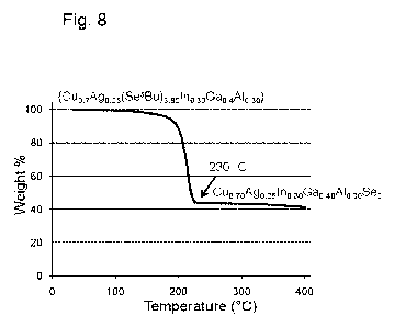
FIG. 8: Fig. 8 shows the transition of a polymeric precursor embodiment (MPP)
of
this invention represented by the repeat unit formula
{Cuo.7Ag0.25(SesBu)3.95In0.3Ga0.4A10.3} into a Cuo.7Ago.251no.3Gao.4Alo.3Se2
material as
determined by thermogravimetric analysis.
FIG. 9: Fig. 9 shows the transition of a polymeric precursor embodiment (MPP)
of
this invention represented by the repeat unit formula
{Cuo.5Ago.5(SesBu)4Ino.7Alo.3}
into a Cuo.5Ago.51no.7A10.3Se2 material as determined by thermogravimetric
analysis.
FIG. 10: Fig. 10 shows the transition of a polymeric precursor embodiment
(MPP) of
this invention represented by the repeat unit formula
{Ago.5oCuo.50(SesBu)4.0A1o.3o1n0.70} into a Ago.5oCuo.5oA1o.3oIn0.70Se2
material as
determined by thermogravimetric analysis.
FIG. 11: Fig. 11 shows the transition of a polymeric precursor embodiment
(MPP) of
this invention represented by the repeat unit formula
{Cuo.9(SesBu)3.9oAlo.251no.5Gao.25}
into a Cu0.9A1o.25Ino.5Gao.25Se2 material as determined by thermogravimetric
analysis.
FIG. 12: Fig. 12 shows the transition of a polymeric precursor embodiment
(MPP) of
this invention represented by the repeat unit formula {Cu(SesBu)4A1} into a
CuAlSe2
material as determined by thermogravimetric analysis.
FIG. 13: Fig. 13 shows the transition of a polymeric precursor embodiment
(MPP) of
this invention represented by the repeat unit formula
{Cuo.9(SesBu)3.9Ga0.7Al0.3} into a
Cu0.9Ga0.7A10.3Se2 material as determined by thermogravimetric analysis.
FIG. 14: Fig. 14 shows the transition of a polymeric precursor embodiment
(MPP) of
this invention represented by the repeat unit formula
{Cuo.9(SesBu)3.9In0.8A10.2} into a
Cuo.9In0.8A10.2Se2 material as determined by thermogravimetric analysis.
9
CA 02768616 2012-01-18
WO 2011/017238 PCT/US2010/044057
FIG. 15: Fig. 15 shows the transition of a polymeric precursor embodiment
(MPP) of
this invention represented by the repeat unit formula {Ag(SesBu)4A1} into a
AgAlSe2
material as determined by thermogravimetric analysis.
FIG. 16: Fig. 16 shows the transition of a polymeric precursor embodiment
(MPP) of
this invention represented by the repeat unit formula {Ag(SesBu)4In0.7Al0.3}
into a
AgIn0.7A10.3Se2 material as determined by thermogravimetric analysis.
FIG. 17: Fig. 17 shows results of methods for stoichiometric control of the
composition of a polymeric precursor embodiment (MPP) of this invention. The x-
axis refers to the weight percent of a particular atom, either Al, In or Ga,
in the
monomer compounds used to prepare the polymeric precursor. The y-axis refers
to
the weight percent of a particular atom in the precursor compound as
synthesized.
The straight line correlation observed in Fig. 17 shows that the stoichiometry
of the
polymeric precursor can be precisely controlled with the quantities of the
monomers
used to make the polymeric precursors.
DETAILED DESCRIPTION
This disclosure provides a range of novel polymeric compounds,
compositions, materials and methods for semiconductor and optoelectronic
materials
and devices including thin film photovoltaics and various semiconductor band
gap
materials.
Among other advantages, the polymeric compounds, compositions, materials
and methods of this invention can provide a precursor compound for making
semiconductor and optoelectronic materials, including CAIGAS absorber layers
for
solar cells and other devices. In some embodiments, the optoelectronic source
precursor compounds of this invention can be used alone, without other
compounds,
to prepare a layer from which CAIGAS and other materials can be made. CAIGAS
refers to (Cu,Ag)(In,Ga,Al)(S,Se), and includes AIGAS, CIGAS and further
materials
described below.
Polymeric precursor compounds may also be used in a mixture with additional
compounds to control stoichiometry of a layer or material.
CA 02768616 2012-01-18
WO 2011/017238 PCT/US2010/044057
In general, the ability to select a predetermined stoichiometry in advance
means that the stoichiometry is controllable.
This invention provides polymeric compounds and compositions for
photovoltaic applications, as well as devices and systems for energy
conversion,
including solar cells.
The polymeric compounds and compositions of this disclosure include
polymeric precursor compounds and polymeric precursors for materials for
preparing
novel semiconductor and photovoltaic materials, films, and products. Among
other
advantages, this disclosure provides stable polymeric precursor compounds for
making and using layered materials and photovoltaics, such as for solar cells
and
other uses.
A photovoltaic absorber material of this disclosure can retain the precise
stoichiometry of the precursor used to make the absorber material.
Polymeric precursors can advantageously form a thin, uniform film. In some
embodiments, a polymeric precursor is an oil that can be processed and
deposited in a
uniform layer on a substrate. This invention provides polymeric precursors
that can
be used neat to make a thin film, or can be processed in an ink composition
for
deposition on a substrate. The polymeric precursors of this invention can have
superior processability to form a thin film for making photovoltaic absorber
layers
and solar cells.
In certain aspects, this invention provides polymeric precursor compounds
having enhanced solubility in organic solvents. The solubility of a polymeric
precursor makes it advantageous for preparing photovoltaic materials using any
one
of various processes that require deposition of the precursor on a substrate,
such as for
making thin film solar cells. A polymeric precursor may have enhanced
solubility in
one or more carriers for preparing an ink to be deposited on a substrate.
In further embodiments, this invention provides a range of polymeric
precursor compounds for which the solubility can advantageously be controlled
and
selectively varied. In these embodiments, the solubility of a polymeric
precursor can
be enhanced by variation of the nature and molecular size and weight of one or
more
organic ligands attached to the compound. The control of polymeric precursor
solubility can allow the preparation of inks having controlled viscosity, for
example,
among other properties.
11
CA 02768616 2012-01-18
WO 2011/017238 PCT/US2010/044057
In general, the structure and properties of the polymeric compounds,
compositions, and materials of this invention provide advantages in making
photovoltaic layers, semiconductors, and devices regardless of the morphology,
architecture, or manner of fabrication of the semiconductors or devices.
The polymeric precursor compounds of this invention are desirable for
preparing semiconductor materials and compositions. A polymeric precursor may
have a chain structure containing two or more different metal atoms which may
be
bound to each other through interactions or bridges with one or more chalcogen
atoms
of chalcogen-containing moieties.
With this structure, when a polymeric precursor is used in a process such as
deposition, coating or printing on a substrate or surface, as well as
processes
involving annealing, sintering, thermal pyrolysis, and other semiconductor
manufacturing processes, use of the polymeric precursors can enhance the
formation
of a semiconductor and its properties.
The polymeric precursor compounds and compositions of this invention may
advantageously be used in processes for solar cells that avoid additional
sulfurization
or selenization steps.
For example, the use of a polymeric precursor in semiconductor
manufacturing processes can enhance the formation of M-E-M' bonding, such as
is
required for chalcogen-containing semiconductor compounds and materials,
wherein
M is an atom of one of Groups 3 to 12, M' is an atom of Group 13, and E is a
chalcogen.
In some embodiments, a polymeric precursor compound may contain a
chalcogenide bridge having the formula MA(E)MA, MB(E)MB or MA(E)MB.
A polymeric precursor compound may advantageously contain linkages
between atoms, where the linkages are desirably found in a material of
interest, such
as a CAIGAS, CIGAS or AIGAS material, which can be made from the polymeric
precursor, or a combination of polymeric precursors.
The polymeric precursor compounds of this disclosure are stable and
advantageously allow control of the stoichiometry, structure, and ratios of
the atoms
in a semiconductor material or layer, in particular, the metal atoms.
Using polymeric precursor compounds in any particular semiconductor
manufacturing process, the stoichiometry of the metal atoms can be determined
and
controlled. The structure of a polymeric precursor may contain a number of
different
12
CA 02768616 2012-01-18
WO 2011/017238 PCT/US2010/044057
metal atoms. Polymeric precursors having different metal atoms, and different
numbers of metal atoms can be contacted in precise amounts to control the
metal atom
stoichiometry in a semiconductor manufacturing process. For processes
operating at
relatively low temperatures, such as certain printing, spraying, and
deposition
methods, the polymeric precursor compounds can maintain the desired
stoichiometry.
As compared to processes involving multiple sources for semiconductor
preparation,
the polymeric precursors of this invention can provide enhanced control of the
uniformity and properties of a semiconductor material.
These advantageous features allow enhanced control over the structure of a
semiconductor material made with the polymeric precursor compounds of this
invention. The polymeric precursors of this disclosure can be superior
building
blocks for semiconductor materials.
The polymeric precursor compounds, compositions and methods of this
disclosure may allow direct and precise control of the stoichiometric ratios
of metal
atoms. For example, in some embodiments, a polymeric precursor can be used
alone,
without other compounds, to readily prepare a layer from which CAIGAS, CIGAS
or
AIGAS materials of any arbitrary stoichiometry can be made.
In certain aspects, polymeric precursor compounds can be used to form
nanoparticles that can be used in various methods to prepare semiconductor
materials.
Embodiments of this invention may further provide processes using
nanoparticles
made from polymeric precursors to enhance the formation and properties of a
semiconductor material.
In aspects of this invention, chemically and physically uniform semiconductor
layers can be prepared with polymeric precursor compounds. The compounds and
compositions of this disclosure are useful to prepare semiconductor layers
having
enhanced properties.
In further embodiments, solar cells and other products can be made in
processes operating at relatively low temperatures using the polymeric
precursor
compounds and compositions of this disclosure.
The polymeric precursors of this disclosure are useful to prepare inks that
can
be used in various methods to prepare semiconductor materials. For processes
involving inks of polymeric precursors, this disclosure can provide enhanced
processability for solar cell production.
13
CA 02768616 2012-01-18
WO 2011/017238 PCT/US2010/044057
Certain polymeric precursor compounds and compositions of this disclosure
provide the ability to be processed at relatively low temperatures, as well as
the ability
to use a variety of substrates including flexible polymers in solar cells.
Embodiments of polymeric precursors for CAIGAS absorbers for solar cells
Embodiments of this invention include:
A compound comprising repeating units {MB(ER)(ER)} and {MA(ER)(ER)},
wherein each MA is Cu or Ag, each MB is In, Ga or Al, each E is S, Se, or Te,
and R is
independently selected, for each occurrence, from alkyl, aryl, heteroaryl,
alkenyl,
amido, silyl, and inorganic and organic ligands. Each E can be sulfur or
selenium. A
compound may be a CAIGAS, AIGAS or CIGAS precursor compound.
A compound comprising two or more repeating units {MB(ER)(ER)} and two
or more repeating units {MA(ER)(ER)}, wherein each MA is Cu or Ag, each MB is
In,
Ga or Al, each E is S, Se, or Te, and R is independently selected, for each
occurrence,
from alkyl, aryl, heteroaryl, alkenyl, amido, silyl, and inorganic and organic
ligands.
A compound comprising repeating units {MB(ER)(ER)} or {MA(ER)(ER)},
wherein each MA is Cu or Ag, each MB is In, Ga or Al, each E is S, Se, or Te,
and R is
independently selected, for each occurrence, from alkyl, aryl, heteroaryl,
alkenyl,
amido, silyl, and inorganic and organic ligands.
A polymeric compound comprising repeating units {MB(ER)(ER)} and
{MA(ER)(ER)}, wherein each MA is Cu or Ag, each MB is In, Ga or Al, each E is
S,
Se, or Te, and R is independently selected, for each occurrence, from alkyl,
aryl,
heteroaryl, alkenyl, amido, silyl, and inorganic and organic ligands.
A compound may have the empirical formula
(Cui_XAgX)õ(Ini_y_tGayAlt)v((Si_zSez)R),,,, wherein x is from 0 to 1, y is
from 0 to 1, t is
from 0 to 1, the sum of y plus t is from 0 to 1, z is from 0 to 1, u is from
0.5 to 1.5, v
is from 0.5 to 1.5, w is from 2 to 6, and R represents R groups, of which
there are w in
number, which are independently selected from alkyl, aryl, heteroaryl,
alkenyl, amido,
silyl, and inorganic and organic ligands. A compound above wherein x is from 0
to
0.5, y is from 0 to 1, t is from 0 to 1, the sum of y plus t is from 0 to 1, z
is from 0 to
1, u is from 0.7 to 1.1, v is from 0.9 to 1.2, and w is from 2 to 6. A
compound above
wherein x is from 0 to 0.3, y is from 0 to 1, t is from 0 to 1, the sum of y
plus t is from
0 to 1, z is from 0 to 1, a is from 0.7 to 1. 1, v is 1, and w is from 3 to 5.
A compound
14
CA 02768616 2012-01-18
WO 2011/017238 PCT/US2010/044057
above wherein x is from 0 to 0.2, y is from 0 to 1, t is from 0 to 1, the sum
of y plus t
is from 0 to 1, z is from 0 to 1, u is from 0.7 to 1.1, v is 1, and w is from
3.5 to 4.5.
A compound may be an inorganic polymer or coordination polymer. A
compound may be linear, branched, cyclic, or a mixture of any of the
foregoing. Each
R may be independently selected, for each occurrence, from (C1-8)alkyl. A
compound may be an oil at a temperature below about 100 C. A compound may
have three or more repeating units {MB(ER)(ER)}. A compound may have three or
more repeating units {MA(ER)(ER)}.
A compound can have the formula (AB), wherein A is the repeat unit
{MA(ER)(ER)}, B is the repeat unit {MB(ER)(ER)}, n is one or more, or n is two
or
more, or n is three or more, and R is independently selected, for each
occurrence, from
alkyl, aryl, heteroaryl, alkenyl, amido, silyl, and inorganic and organic
ligands. A
compound can be an alternating copolymer, a block copolymer, or a random
copolymer.
A compound can have any one of the formulas: (RE)2-BB(AB),,,
(RE)2-B(AB)õB, (RE)2-B(AB)õ B(AB)m, (RE)2-(BA)õBB, (RE)2-B(BA)õB,
(RE)2-(BA).B(BA)mB, cyc"c(AB)õ cyc"c(BA),,, (RE)2-(BB)(AABB),,,
(RE)2-(BB)(AABB)n(AB)m, (RE)2-(B)(AABB)n(B)(AB)m, (RE)2-[B(AB)n] ,
(RE)2-[(BA)nB],
R
ER
B
MA' M
EC
\ER
R
R R R R
!E E~ E E
Mp MB1 M A MB2
E/ E
R R R R
P
CA 02768616 2012-01-18
WO 2011/017238 PCT/US2010/044057
R R R R
E E E~ E
MAI MB1 MA2 MB2
E/ Y R R R
====== L B'AIB2 AB3 ======
(RE)2-BB(AB1)n(AB2)r,,, (RE)2-BB(AB1)n(AB2) (ABi)p,
(RE)2-BB(AB1)n(AB2)rõ(AB1)p, (RE)2-BB(A1B)n(A2B)r,,,
(RE)2-BB(A1B)õ (A2B)m(A1B)p, and a mixture of any of the foregoing, wherein A
is
the repeat unit {MA(ER)(ER)}, B is the repeat unit {MB(ER)(ER)}, p is one or
more,
n is one or more, or n is two or more, or n is three or more, and m is one or
more.
A compound may have any one of the repeat unit formulas:
{CU0.7Ag0.25(SesBU)3.951n0.3Ga0.4A10.3}, {Ga0.5Al0.5(SesBU)3.9CU0.5Ag0.4},
{CU0.5Ag0.5(SesBU)41n0.7A10.3}, {Cu0.91n0.5Ga0.25A10.25(SesBU)3.9},
{Cu(SesBu)4Al},
{Cu0.9(SesBu)3.9Ga0.7Al0.3}, {Cu0.9(SesBu)3.9In0.8Al0.2}, {Ag(SesBU)4Al},
{Ag(SesBu)4In0.7Al0.3}, {Cuo.5Ago.5(SesBu)4(In,Ga,Al)},
{Cuo.7Ago.i(SesBu)3.8Gao.21n0.7A10.i}, {Cuo.8Ago.2(SesBu)4(In,Ga,Al)},
{Cuo.2Ag0.8(SesBu)4(In,Ga,Al)}, {Cuo.5Ago.5(SesBu)4Gao.451no.5A1o.05},
{Cuo.85Ago. i(SesBu)3.95Gao.i51no.7A1o.i5}, {Cuo.5Ago.5(SesBu)4Gao.31no.7
Alo.oi},
{Cuo.8Ago.o5(SesBu)3.85Gao.31no.3Alo.4}, {(Cu,Ag)(SetBu)(SeBu)(In,Ga,Al)(Se"
Bu)2},
{(Cu,Ag)(StBu)(S'Pr)(In,Ga,Al)(S'Pr)2},
{Cui.4oAgo.io(SetBu)i.5(Se'Bu)(Ino.7Gao.25Alo.o5)(Se" Bu)2};
{Cui.3oAgo.io(StBu)i.4(StBu)(Ino.85Gao.iAlo.o5)(StBu)2};
{Cui.2oAgo.io(StBu)i.3(S'Bu)(Ino.8oGao.i5A1o.o5)(S'Bu)2}
{Cui.ioAgo.io(SetBu)i.2(Se'Bu)(Ino.75Gao.2oA1o.o5)(Se" Bu)2};
{Cui.o5Ago.05(StBu)i.i(SetBu)(Ino.7Gao.2Alo.i)(SetBu)2},
{Cuo.9oAgo.io(SetBu)(Se"Bu)(Ino.7Gao.25A10.05)(Se"Bu)2};
{Cuo.85Ago.io(StBu)o.95(StBu)(Ino.85Gao.iAlo.o5)(StBu)2};
{Cuo.8oAgo.2o(StBu)(S"Bu)(Ino.8oGao.i5Alo.o5)(S" Bu)2};
{Cuo.75Ago.2o(SetBu)o.95(Se"Bu)(Ino.75Gao.2oAlo.o5)(Se" Bu)2};
{Cuo.7oAgo.30(StBu)(SetBu)(Ino.7Gao.2Alo.i)(SetBu)2};
{Cuo.65Ago.30(SetBu)o.95(StBu)(Ino.6Gao.3Alo.i)(StBu)2};
16
CA 02768616 2012-01-18
WO 2011/017238 PCT/US2010/044057
{Cuo.6oAgo.4o(SetBu)2(Ino.5Gao.4Alo.i)(SetBu)2};
{Cuo.5oAgo.5o(SetBu)(SeBu)(In0.5Ga0.4Alo.i)(Se'Bu)2};
{Cuo.3oAgo.65(StBu)o.95(StBu)(Ino.5Gao.4Alo.i)(StBu)2};
{Cuo.3oAgo.7o(StBu)(S" Bu)(Ino.4Gao.5Alo.i)(S" Bu)2};
{Cuo.2oAgo.75(SetBu)o.95(SeBu)(Ino.4Gao.5Alo.i)(Se"Bu)2};
{Cuo.2oAgo.so(StBu)(SetBu)(In0.3Gao.1Al0.6)(SetBu)2};
{Cuo.ioAgo.85(SetBu)o.95(StBu)(Ino.3Gao.6Alo.i)(StBu)2}; and
{Cuo.ioAgo.9o(SetBu)2(Ino.2Gao.7Alo.i)(SetBu)2} .
An ink comprising one or more compounds above and one or more carriers.
An ink may be a solution of the compounds in an organic carrier. An ink may
contain
a dopant or alkali dopant. An ink may contain one or more components selected
from
the group of a surfactant, a dispersant, an emulsifier, an anti-foaming agent,
a dryer, a
filler, a resin binder, a thickener, a viscosity modifier, an anti-oxidant, a
flow agent, a
plasticizer, a conductivity agent, a crystallization promoter, an extender, a
film
conditioner, an adhesion promoter, and a dye. An ink can contain one or more
components selected from the group of a conducting polymer, silver metal,
silver
selenide, silver sulfide, copper metal, indium metal, gallium metal, zinc
metal, an
alkali metal, an alkali metal salt, an alkaline earth metal salt, a sodium
chalcogenate, a
calcium chalcogenate, cadmium sulfide, cadmium selenide, cadmium telluride,
indium sulfide, indium selenide, indium telluride, gallium sulfide, gallium
selenide,
gallium telluride, zinc sulfide, zinc selenide, zinc telluride, copper
sulfide, copper
selenide, copper telluride, molybdenum sulfide, molybdenum selenide,
molybdenum
telluride, and mixtures of any of the foregoing.
A method for making a precursor compound comprising:
a) providing monomer compounds MBi(ER)3, MB2(ER)3, MB3(ER)3, MAT(ER)
and MA2 (ER); and
b) contacting the monomer compounds;
wherein MBi is In, MB2 is Ga, MB3 is Al, MAi is Cu, and MA2 is Ag, each E is
S, Se, or
Te, and each R is independently selected, for each occurrence, from alkyl,
aryl,
heteroaryl, alkenyl, amido, silyl, and inorganic and organic ligands. MAI and
MA2
may both be Cu, or MAI and MA2 can both be Ag. Each E is sulfur or selenium.
The
compound may be a CAIGAS, AIGAS or CIGAS precursor compound. The
compound can be deficient in a Group 11 atom. The monomer compounds may be
contacted in a process of depositing, spraying, coating, or printing. The
monomer
17
CA 02768616 2012-01-18
WO 2011/017238 PCT/US2010/044057
compounds can be contacted at a temperature of from about -60 C to about 100
C,
or from about 0 C to about 200 C.
A compound made by a process comprising reacting monomers MBi(ER)3,
MB2(ER)3, MB3(ER)3, MAT(ER) and MA2 (ER), wherein MBi is In, MB2 is Ga, MB3 is
Al, MAi is Cu, and MA2 is Ag, each E is S, Se, or Te, and R is independently
selected,
for each occurrence, from alkyl, aryl, heteroaryl, alkenyl, amido, silyl, and
inorganic
and organic ligands. The compound above wherein MAi and MA2 are both Cu, or
MAi
and MA2 are both Ag. The compound above wherein each E is sulfur or selenium.
The compound above wherein the compound is a CAIGAS, AIGAS or CIGAS
precursor compound. The compound above wherein the compound has the empirical
formula (Cui_XAgX)õ(Ini_y_tGayAlt)v((Si_zSez)R),,,, wherein x is from 0 to 1,
y is from 0
to 1, t is from 0 to 1, the sum of y plus t is from 0 to 1, z is from 0 to 1,
u is from 0.5
to 1.5, v is from 0.5 to 1.5, w is from 2 to 6, and R represents R groups, of
which there
are w in number, which are independently selected from alkyl, aryl,
heteroaryl,
alkenyl, amido, silyl, and inorganic and organic ligands. The compound above
wherein x is from 0 to 0.5, y is from 0 to 1, t is from 0 to 1, the sum of y
plus t is from
O to 1, z is from 0 to 1, a is from 0.7 to 1. 1, v is from 0.9 to 1.2, and w
is from 2 to 6.
The compound above wherein x is from 0 to 0.3, y is from 0 to 1, t is from 0
to 1, the
sum of y plus t is from 0 to 1, z is from 0 to 1, u is from 0.7 to 1.1, v is
1, and w is
from 3 to 5. The compound above wherein x is from 0 to 0.2, y is from 0 to 1,
t is
from 0 to 1, the sum of y plus t is from 0 to 1, z is from 0 to 1, u is from
0.7 to 1.1, v
is 1, and w is from 3.5 to 4.5.
An article comprising one or more compounds or inks described above
deposited onto a substrate. The article above wherein the depositing is done
by
spraying, spray coating, spray deposition, spray pyrolysis, printing, screen
printing,
inkjet printing, aerosol jet printing, ink printing, jet printing, stamp/pad
printing,
transfer printing, pad printing, flexographic printing, gravure printing,
contact
printing, reverse printing, thermal printing, lithography, electrophotographic
printing,
electrodepositing, electroplating, electroless plating, bath deposition,
coating, wet
coating, spin coating, knife coating, roller coating, rod coating, slot die
coating,
meyerbar coating, lip direct coating, capillary coating, liquid deposition,
solution
deposition, layer-by-layer deposition, spin casting, solution casting, and
combinations
of any of the forgoing. The article above wherein the substrate is selected
from the
group of a semiconductor, a doped semiconductor, silicon, gallium arsenide,
18
CA 02768616 2012-01-18
WO 2011/017238 PCT/US2010/044057
insulators, glass, molybdenum glass, silicon dioxide, titanium dioxide, zinc
oxide,
silicon nitride, a metal, a metal foil, molybdenum, aluminum, beryllium,
cadmium,
cerium, chromium, cobalt, copper, gallium, gold, lead, manganese, molybdenum,
nickel, palladium, platinum, rhenium, rhodium, silver, stainless steel, steel,
iron,
strontium, tin, titanium, tungsten, zinc, zirconium, a metal alloy, a metal
silicide, a
metal carbide, a polymer, a plastic, a conductive polymer, a copolymer, a
polymer
blend, a polyethylene terephthalate, a polycarbonate, a polyester, a polyester
film, a
mylar, a polyvinyl fluoride, polyvinylidene fluoride, a polyethylene, a
polyetherimide,
a polyethersulfone, a polyetherketone, a polyimide, a polyvinylchloride, an
acrylonitrile butadiene styrene polymer, a silicone, an epoxy, paper, coated
paper, and
combinations of any of the forgoing. The article above wherein the substrate
is a
shaped substrate including a tube, a cylinder, a roller, a rod, a pin, a
shaft, a plane, a
plate, a blade, a vane, a curved surface or a spheroid.
A method for making an article, the method comprising:
(a) providing one or more compounds or inks described above;
(b) providing a substrate; and
(c) depositing the compounds or inks onto the substrate.
The method above wherein step (c) is repeated. The method above further
comprising
heating the substrate at a temperature of from about 100 C to about 400 C to
convert
the compounds or inks to a material. The method above further comprising
heating
the substrate at a temperature of from about 100 C to about 400 C to convert
the
compounds or inks to a material, followed by repeating step (c). The method
above
further comprising annealing the material by heating the substrate at a
temperature of
from about 300 C to about 650 C. The method above further comprising heating
the
substrate at a temperature of from about 100 C to about 400 C to convert the
compounds or inks to a material, and annealing the material by heating the
substrate
at a temperature of from about 300 C to about 650 C. The method above further
comprising heating the substrate at a temperature of from about 100 C to about
400 C
to convert the compounds or inks to a material, depositing the compounds or
inks
onto the substrate, and annealing the material by heating the substrate at a
temperature
of from about 300 C to about 650 C.
The method above further comprising:
(d) heating the substrate at a temperature of from about 100 C to about 400 C
to convert the compounds or inks to a material;
19
CA 02768616 2012-01-18
WO 2011/017238 PCT/US2010/044057
(e) depositing the compounds or inks onto the substrate;
(f) repeating steps (d) and (e); and
(g) annealing the material by heating the substrate at a temperature of from
about 300 C to about 650 C.
The method above further comprising:
(d) heating the substrate at a temperature of from about 100 C to about 400 C
to convert the compounds or inks to a material;
(e) annealing the semiconductor material by heating the substrate at a
temperature of from about 300 C to about 650 C; and
(f) repeating steps (c), (d) and (e).
The method above further comprising an optional step of selenization or
sulfurization,
either before, during or after any step of heating or annealing.
A material having the empirical formula
(Cui_XAg,,)õ(Ini_y_tGayAlt)v(Si_zSez)W,
where xis from 0 to 1, y is from 0 to 1, t is from 0.001 to 1, the sum of y
plus t is
from 0.001 to 1, z is from 0 to 1, u is from 0.5 to 1.5, v is from 0.5 to 1.5,
and w is
from 1 to 3. The material above wherein x is from 0 to 0.5, y is from 0 to 1,
t is from
0.001 to 0.5, z is from 0.5 to 1, u is from 0.7 to 1.1, v is from 0.9 to 1.1,
and w is from
1.8 to 2.4. The material above wherein x is from 0 to 0.3, y is from 0 to 1, t
is from
0.001 to 0.3, z is from 0.5 to 1, u is from 0.7 to 1.1, v is 1, and w is from
1.8 to 2.4.
The material above wherein x is from 0 to 0.2, y is from 0 to 1, t is from
0.001 to 0.2,
z is from 0.5 to 1, u is from 0.7 to 1.1, v is 1, and w is from 2.0 to 2.4.
The material
above wherein the material is a semiconductor. The material above wherein the
material is in the form of a thin film. An optoelectronic device comprising
the
material above.
A method for making a material comprising,
(a) providing one or more compounds or inks above;
(b) providing a substrate;
(c) depositing the compounds or inks onto the substrate; and
(d) heating the substrate at a temperature of from about 20 C to about 650 C
in an inert atmosphere, thereby producing a material having a thickness of
from 0.001
to 100 micrometers. The method above wherein the substrate is heated at a
temperature of from about 100 C to about 550 C, or from about 200 C to
about
400 C. A photovoltaic device comprising a material made by the method above.
CA 02768616 2012-01-18
WO 2011/017238 PCT/US2010/044057
A thin film material made by a process comprising,
(a) providing one or more compounds or inks above;
(b) providing a substrate;
(c) depositing the compounds or inks onto the substrate; and
(d) heating the substrate at a temperature of from about 20 C to about 650 C
in an inert atmosphere, thereby producing a thin film material having a
thickness of
from 0.001 to 100 micrometers. The thin film material above wherein the
substrate is
heating at a temperature of from about 100 C to about 550 C, or from about
200 C
to about 400 C. The thin film material above, the process further comprising
an
optional step of selenization or sulfurization, either before, during or after
steps (c) or
(d). A photovoltaic absorber made with a thin film material above. A
photovoltaic
device comprising a thin film material above.
A photovoltaic absorber having the empirical formula
(Cui_XAg,,)õ(Ini_y_tGayAlt)v(Si_zSez)W, where x is from 0 to 1, y is from 0 to
1, t is from
0.001 to 1, the sum of y plus t is from 0.001 to 1, z is from 0 to 1, u is
from 0.5 to 1.5,
v is from 0.5 to 1.5, and w is from 1 to 3. The photovoltaic absorber above
wherein x
is from 0 to 0.5, y is from 0 to 1, t is from 0.001 to 0.5, z is from 0.5 to
1, u is from
0.7 to 1.1, v is from 0.9 to 1.1, and w is from 1.8 to 2.4. The photovoltaic
absorber
above wherein x is from 0 to 0.3, y is from 0 to 1, t is from 0.001 to 0.3, z
is from 0.7
to 1, u is from 0.7 to 1.1, v is 1, and w is from 1.8 to 2.4. The photovoltaic
absorber
above wherein x is from 0 to 0.2, y is from 0 to 1, t is from 0.001 to 0.2, z
is from 0.8
to 1, u is from 0.7 to 1.1, v is 1, and w is from 2.0 to 2.4. A photovoltaic
device
comprising the photovoltaic absorber above. A system for providing electrical
power
comprising a photovoltaic device above. A method for providing electrical
power
comprising using a photovoltaic system above to convert light into electrical
energy.
A method for making a photovoltaic absorber layer on a substrate comprising,
(a) providing one or more compounds or inks above;
(b) providing a substrate;
(c) depositing the compounds or inks onto the substrate; and
(d) heating the substrate at a temperature of from about 100 C to about
650 C in an inert atmosphere, thereby producing a photovoltaic absorber layer
having a thickness of from 0.001 to 100 micrometers. The method above wherein
the
substrate is heating at a temperature of from about 100 C to about 550 C, or
from
about 200 C to about 400 C. The method above further comprising an optional
step
21
CA 02768616 2012-01-18
WO 2011/017238 PCT/US2010/044057
of selenization or sulfurization, either before, during or after steps (c) or
(d). A
photovoltaic device comprising a photovoltaic absorber layer made by the
method
above.
Empirical formulas of precursor compounds
This disclosure provides a range of polymeric precursor compounds having
two or more different metal atoms and chalcogen atoms.
In certain aspects, a polymeric precursor compound contains metal atoms, and
atoms of Group 13, as well as combinations thereof. Any of these atoms may be
bonded to one or more atoms selected from atoms of Group 15, S, Se, and Te, as
well
as one or more ligands.
A polymeric precursor compound may be a neutral compound, or an ionic
form, or have a charged complex or counterion. In some embodiments, an ionic
form
of a polymeric precursor compound may contain a divalent metal atom, or a
divalent
metal atom as a counterion.
A polymeric precursor compound may contain atoms selected from the
transition metals of Group 3 through Group 12, B, Al, Ga, In, Tl, Si, Ge, Sn,
Pb, As,
Sb, and Bi. Any of these atoms may be bonded to one or more atoms selected
from
atoms of Group 15, S, Se, and Te, as well as one or more ligands.
A polymeric precursor compound may contain atoms selected from Ni, Pd, Pt,
Cu, Ag, An, Zn, Cd, Hg, B, Al, Ga, In, Tl, Si, Ge, Sn, Pb, and Bi. Any of
these atoms
may be bonded to one or more atoms selected from atoms of Group 15, S, Se, and
Te,
as well as one or more ligands.
In some embodiments, a polymeric precursor compound may contain atoms
selected from Cu, Ag, Zn, Ga, In, Al, Tl, Si, Ge, Sn, and Pb. Any of these
atoms may
be bonded to one or more atoms selected from atoms of Group 15, S, Se, and Te,
as
well as one or more ligands.
In some embodiments, a polymeric precursor compound may contain atoms
selected from Cu, Ag, Zn, Ga, In, Al, Tl, Si, Ge, Sn, and Pb. Any of these
atoms may
be bonded to one or more chalcogen atoms, as well as one or more ligands.
In some variations, a polymeric precursor compound may contain atoms
selected from Cu, Ag, In, Ga and Al. Any of these atoms may be bonded to one
or
more atoms selected from S, Se, and Te, as well as one or more ligands.
22
CA 02768616 2012-01-18
WO 2011/017238 PCT/US2010/044057
Polymeric precursor structure and properties (MPP-CAIGAS)
A polymeric precursor compound of this disclosure can be stable at ambient
temperatures. Polymeric precursors can be used for making layered materials,
optoelectronic materials, and devices. Using polymeric precursors
advantageously
allows control of the stoichiometry, structure, and ratios of various atoms in
a
material, layer, or semiconductor.
Polymeric precursor compounds of this invention may be solids, solids with
low melting temperatures, semisolids, flowable solids, gums, or rubber-like
solids,
oily substances, or liquids at ambient temperatures, or temperatures
moderately
elevated from ambient. Embodiments of this disclosure that are fluids at
temperatures
moderately elevated from ambient can provide superior processability for
production
of solar cells and other products, as well as the enhanced ability to be
processed on a
variety of substrates including flexible substrates.
In general, a polymeric precursor compound can be processed through the
application of heat, light, kinetic, mechanical or other energy to be
converted to a
material, including a semiconductor material. In these processes, a polymeric
precursor compound undergoes a transition to become a material. The conversion
of
a polymeric precursor compound to a material can be done in processes known in
the
art, as well as the novel processes of this disclosure.
Embodiments of this invention may further provide processes for making
optoelectronic materials. Following the synthesis of a polymeric precursor
compound, the compound can be deposited, sprayed, or printed onto a substrate
by
various means. Conversion of the polymeric precursor compound to a material
can be
done during or after the process of depositing, spraying, or printing the
compound
onto the substrate.
A polymeric precursor compound of this disclosure may have a transition
temperature below about 400 C, or below about 300 C, or below about 280 C,
or
below about 260 C, or below about 240 C, or below about 220 C, or below
about
200 C.
In some aspects, polymeric precursors of this disclosure include molecules
that are melt processable at temperatures below about 100 C. In certain
aspects, a
polymeric precursor can be fluid, flowable, flowable melt, or semisolid at
relatively
low temperatures and can be processed as a neat solid, semisolid, neat
flowable melt,
23
CA 02768616 2012-01-18
WO 2011/017238 PCT/US2010/044057
flowable solid, gum, rubber-like solid, oily substance, or liquid. In certain
embodiments, a polymeric precursor is melt processable as a flowable melt at a
temperature below about 200 C, or below about 180 C, or below about 160 C,
or
below about 140 C, or below about 120 C, or below about 100 C, or below
about
80 C, or below about 60 C, or below about 40 C.
A polymeric precursor compound of this invention can be crystalline or
amorphous, and can be soluble in various non-aqueous solvents.
A polymeric precursor compound may contain ligands, or ligand fragments, or
portions of ligands that can be removed under mild conditions, at relatively
low
temperatures, and therefore provide a facile route to convert the polymeric
precursor
to a material or semiconductor. The ligands, or some atoms of the ligands, may
be
removable in various processes, including certain methods for depositing,
spraying,
and printing, as well as by application of energy.
These advantageous features allow enhanced control over the structure of a
semiconductor material made with the polymeric precursor compounds of this
invention.
Polymeric precursors for semiconductors and optoelectronics (MPP-CAIGAS)
This invention provides a range of polymeric precursor structures,
compositions, and molecules having two or more different metal atoms.
In some embodiments, a polymeric precursor compound contains atoms MB of
Group 13 selected from Ga, In, Al, and a combination thereof.
The atoms MB may be any combination of atoms of Ga, In and Al.
These polymeric precursor compounds further contain monovalent metal
atoms MA selected from Cu, Ag, and a mixture thereof.
The atoms MA may be any combination of atoms of Cu and Ag.
The polymeric precursors of this disclosure can be considered inorganic
polymers or coordination polymers.
The polymeric precursors of this disclosure may be represented in different
ways, using different formulas to describe the same structure.
In some aspects, a polymeric precursor of this disclosure may be a
distribution
of polymer molecules or chains. The distribution may encompass molecules or
chains
having a range of chain lengths or molecular sizes. A polymeric precursor can
be a
mixture of polymers, polymer molecules or chains. The distribution of a
polymeric
24
CA 02768616 2012-01-18
WO 2011/017238 PCT/US2010/044057
precursor can be centered or weighted about a particular molecular weight or
chain
mass.
Embodiments of this invention further provide polymeric precursors that can
be described as AB alternating addition copolymers.
The AB alternating addition copolymer is in general composed of repeat units
A and B. The repeat units A and B are each derived from a monomer. The repeat
units A and B may also be referred to as being monomers, although the
empirical
formula of monomer A is different from the empirical formula of repeat unit A.
The monomer for MA can be MA(ER), where MA is Cu or Ag.
The monomer for MB can be MB(ER)3, where MB is Ga, In, Al, or any mixture
of Ga, In and Al.
In a polymeric precursor, monomers of A link to monomers of B to provide a
polymer chain, whether linear, cyclic, or branched, or of any other shape,
that has
repeat units A, each having the formula {MA(ER)2}, and repeat units B, each
having
the formula {MB(ER)2}. The repeat units A and B may appear in alternating
order in
the chain, for example, ===ABABABABAB===.
In some embodiments, a polymeric precursor may have atoms MB of Ga, In
and Al where the different atoms appear in random order in the structure.
The polymeric precursor compounds of this invention may be made with any
desired stoichiometry with respect to the number of different Group 13
elements and
their respective ratios. The stoichiometry of a polymeric precursor compound
may be
controlled through the concentrations of monomers, or repeating units in the
polymer
chains of the precursors. A polymeric precursor compound may be made with any
desired stoichiometry with respect to the number of different Group 13
elements and
their respective ratios.
In some aspects, this disclosure provides polymeric precursors which are
inorganic AB alternating addition copolymers having one of the following
Formulas 1
through 13:
Formula 1: (RE)2-[B(AB)õ]
Formula 2: (RE)2-[(BA)õ B]
Formula 3: (RE)2-BB(AB)õ
Formula 4: (RE)2-B(AB)õ B
CA 02768616 2012-01-18
WO 2011/017238 PCT/US2010/044057
Formula 5: (RE)2-B(AB)õ B(AB)m
Formula 6: (RE)2-(BA)õBB
Formula 7: (RE)2-B(BA)õB
Formula 8: (RE)2-(BA)õB(BA).B
Formula 9: y i' (AB)õ
Formula 10: y h1c(BA)õ
Formula 11: (RE)2-(BB)(AABB)õ
Formula 12: (RE)2-(BB)(AABB)n(AB),,,
Formula 13: (RE)2-(B)(AABB)n(B)(AB),,,
where A and B are as defined above, E is S, Se, or Te, and R is defined below.
Formulas 1 and 2 describe ionic forms that have a counterion or counterions
not shown. Examples of counterions include alkali metal ions, Na, Li, and K.
The formulas RE-B(AB)õ and RE-(BA)õ B may describe stable molecules
under certain conditions.
For example, an embodiment of a polymeric precursor compound of Formula
4 is shown in Fig. 1. As shown in Fig. 1, the structure of the compound can be
represented by the formula (RE)2BABABB, wherein A is the repeat unit
{MA(ER)2},
B is the repeat unit {MB(ER)2}, E is a chalcogen, and R is a functional group
defined
below.
In another example, an embodiment of a polymeric precursor compound of
Formula 5 is shown in Fig. 2. As shown in Fig. 2, the structure of the
compound can
be represented by the formula (RE)2BABABBABAB, wherein A is the repeat unit
{MA(ER)2}, B is the repeat unit {MB(ER)2}, E is a chalcogen, and R is a
functional
group defined below.
In a further example, an embodiment of a polymeric precursor compound of
Formula 6 is shown in Fig. 3. As shown in Fig. 3, the structure of the
compound can
be represented by the formula (RE)2BA(BA)õ BB, wherein A is the repeat unit
{MA(ER)2}, B is the repeat unit {MB(ER)2}, E is a chalcogen, and R is a
functional
group defined below.
In another example, an embodiment of a polymeric precursor compound of
Formula 8 is shown in Fig. 4. As shown in Fig. 4, the structure of the
compound can
be represented by the formula (RE)2BA(BA)nB(BA),,,B, wherein A is the repeat
unit
26
CA 02768616 2012-01-18
WO 2011/017238 PCT/US2010/044057
{MA(ER)2}, B is the repeat unit {MB(ER)2}, E is a chalcogen, and R is a
functional
group defined below.
In a further example, an embodiment of a polymeric precursor compound of
Formula 10 is shown in Fig. 5. As shown in Fig. 5, the structure of the
compound can
be represented by the formula y i' (BA)4, wherein A is the repeat unit
{MA(ER)2}, B
is the repeat unit {MB(ER)2}, E is a chalcogen, and R is a functional group
defined
below.
A polymeric precursor having one of Formulas 1-8 and 11-13 may be of any
length or molecular size. The values of n and m can be one (1) or more. In
certain
embodiments, the values of n and m are 2 or more, or 3 or more, or 4 or more,
or 5 or
more, or 6 or more, or 7 or more, or 8 or more, or 9 or more, or 10 or more.
In some
embodiments, n and m are independently from 2 to about one million, or from 2
to
about 100,000, or from 2 to about 10,000, or from 2 to about 5000, or from 2
to about
1000, or from 2 to about 500, or from 2 to about 100, or from 2 to about 50.
A cyclic polymeric precursor having one of Formulas 9 or 10 may be of any
molecular size. The value of n may be two (2) or more. In certain variations,
the
values of n and m are 2 or more, or 3 or more, or 4 or more, or 5 or more, or
6 or
more, or 7 or more, or 8 or more, or 9 or more, or 10 or more. In some
embodiments,
for cyclic Formulas 9 and 10, n is from 2 to about 50, or from 2 to about 20,
or from 2
to about 16, or from 2 to about 14, or from 2 to about 12, or from 2 to about
10, or
from 2 to about 8.
In another aspect, the repeat units {MB(ER)2} and {MA(ER)2} may be
considered "handed" because the metal atom MA and the Group 13 atom MB appear
on the left, while the chalcogen atom E appears to the right side. Thus, a
linear
terminated chain will in general require an additional chalcogen group or
groups on
the left terminus, as in Formulas 1-8 and 11-13, to complete the structure. A
cyclic
chain, as described by Formulas 9 and 10, does not require an additional
chalcogen
group or groups for termination.
In certain aspects, structures of Formulas 1-8 and 11-13, where n and m are
one (1), may be described as adducts. For example, adducts include (RE)2-BBAB,
(RE)2-BABB, and (RE)2-BABBAB.
In some embodiments, a polymeric precursor may include a structure that is an
AABB alternating block copolymer. For example, a polymeric precursor or
portions
of a precursor structure may contain one or more consecutive repeat units
{AABB}.
27
CA 02768616 2012-01-18
WO 2011/017238 PCT/US2010/044057
A polymeric precursor having an AABB alternating block copolymer may be
represented by Formula 11 above.
In some aspects, this disclosure provides polymeric precursors which are
inorganic AB alternating addition copolymers having the repeat units of
Formula 14
R
ER
B
MA M
-EC
\ER
R
Formula 14
where atoms MB are atoms of Group 13 selected from Ga and In, and E is S, Se,
or Te.
In certain aspects, this invention provides polymeric precursors having a
number n of the repeat units of Formula 14, where n may be 1 or more, or 2 or
more,
or 3 or more, or 4 or more, or 5 or more, or 6 or more, or 7 or more, or 8 or
more, or 9
or more, or 10 or more, or 11 or more, or 12 or more.
The AB copolymer of Formula 14 may also be represented as (AB)õ or (BA),,,
which represents a polymer of any chain length. Another way to represent
certain AB
copolymers is the formula ... ABAB===.
In further variations, this invention provides polymeric precursors that may
be
represented by Formula 15
R R R R
!E E~ E E
M p MB1 M A MB2
E/ E
R \ R R R
P
Formula 15
where atoms MB1 and MB2 are the same or different atoms of Group 13 selected
from
Ga, In and Al, E is S, Se, or Te, and p is one (1) or more.
28
CA 02768616 2012-01-18
WO 2011/017238 PCT/US2010/044057
In further aspects, this invention provides polymeric precursors which may be
represented by Formula 16
R R R R
l E E~ 2 MB2 E
MA\ MB1 ME/ E
R R R R
P
Formula 16
where atoms MB1 and MB2 are the same or different atoms of Group 13 selected
from
Ga In and Al, atoms MA1 and MA2 are the same or different and are atoms
selected
from Cu and Ag, E is S, Se, or Te, and p is one (1) or more.
In another aspect, this disclosure provides inorganic AB alternating
copolymers which may be represented by Formula 17
000000 /~R1 /~ 32/~R3 000000
L1FForLmuullaL117L
where B1, B2, and B3 are repeat units containing atoms MB1, MB2, and MB3
respectively, which are atoms of Ga and In.
Certain examples of empirical formulas for monomers and polymeric
precursors of this invention are summarized in Table 1.
Table 1: Empirical formulas for monomers, repeat units and polymeric
precursors
Formula Representative Constitutional Chain Unit Description
From monomer
A {MA(ER)a} MA(ER),
where MA is Cu or
Ag
From monomer
B {MB(ER)a} MB(ER)s,
where MB is Ga, In,
Al
AB {MA(ER)2MB(ER)2} Polymer chain
29
CA 02768616 2012-01-18
WO 2011/017238 PCT/US2010/044057
Formula Representative Constitutional Chain Unit Description
repeat unit
ABA {MA(ER)2MB(ER)2MA(ER)2} An adduct, trimer,
or oligomer
Polymer chain
repeat unit, MB1 and
BIAB2 {MB1(ER)2MA(ER)2MB2(ER)2} MB2 may be the
same or different, a
trimer or oligomer
Alternating
AB1AB2 {MA(ER)2MBI(ER)2MA(ER)2MB2(ER)2} copolymer (AB),,, a
tetramer or oligomer
Polymer, or an AB
AB'AB2AB3 {MA(ER)2MBi(ER)2MA(ER)2MB2(ER)2MA(ER)2MBi(ER)2} trimer, or an
oligomer
or
(AB )n or Pol mer of any
(BA)eA-B_)_ ~B-A) chain length
n n
Polymer of any
===ABAB=== -A B-A By length, whether
linear, branched, or
cyclic
{AABB} ~A-A-B-B-- AABB alternating
block copolymer
A-B\
cyclic (AB)4 or B A Cyclic polymer
cyclic(BA)4 I I chain, oligomer or
A B octamer
\B-A/
In Table 1, the "representative constitutional chain unit" refers to the
repeating
unit of the polymer chain. In general, the number and appearance of electrons,
ligands, or R groups in a representative constitutional chain repeating unit
does not
necessarily reflect the oxidation state of the metal atom. For example, the
chain repeating
unit A, which is {MA(ER)2}, arises from the monomer MA(ER), where MA is a
metal
atom of monovalent oxidation state 1 (I or one) selected from Cu and Ag. It is
to be
understood that the repeating unit exists in the polymer chain bonded to two
other repeating
units, or to a repeating unit and a chain terminating unit. Likewise, the
chain repeating unit B,
which is {MB(ER)2}, arises from the monomer MB(ER)3, where MB is a Group 13
atom of trivalent oxidation state 3 (III or three) selected from Ga, In, Al,
and a
CA 02768616 2012-01-18
WO 2011/017238 PCT/US2010/044057
mixture thereof. In one aspect, monomer MA(ER), and monomer MB(ER)3, combine
to form an AB repeating unit, which is {MA(ER)2MB(ER)2}.
In some aspects, this disclosure provides AB alternating copolymers which
may also be alternating with respect to MA or MB. A polymeric precursor that
is
alternating with respect to MA may contain chain regions having alternating
atoms
MAl and MA2. A polymeric precursor that is alternating with respect to MB may
contain chain regions having alternating atoms MB1 and MB2.
In further aspects, this disclosure provides AB alternating block copolymers
which may contain one or more blocks of n repeat units, represented as (AB')õ
or
(B1A),,, where the block of repeat units contains only one kind of atom MBi
selected
from Group 13. A block may also be a repeat unit represented as (A1B)õ or
(BA),,,
where the block of repeat units contains only one kind of atom MAi. A
polymeric
precursor of this disclosure may contain one or more blocks of repeat units
having
different Group 13 atoms in each block, or different atoms MA in each block.
For
example, a polymeric precursor may have one of the following formulas:
Formula 18: (RE)2-BB(ABl),,(AB2)m
Formula 19: (RE)2-BB(AB1),,(AB2)m(AB1)p
Formula 20: (RE)2-BB(AB1),,(AB2)m(AB1)p
Formula 21: (RE)2-BB(A1B),,(A2B)m
Formula 22: (RE)2-BB(A1B)n(A2B)m(A1B)p
where B1, B2 represent repeat units {MB'(ER)2} and {MB2(ER)2}, respectively,
where
MBi, MB2 are In, Ga, respectively, and where Ai, A2 represent repeat units
{MAi(ER)2} and {MA2(ER)2}, respectively, where MAi, MA2 are Cu and Ag,
respectively. In Formulas 18 through 22, the values of n, m, and p may be 2 or
more,
or 3 or more, or 4 or more, or 5 or more, or 6 or more, or 7 or more, or 8 or
more, or 9
or more, or 10 or more, or 11 or more, or 12 or more.
In certain embodiments, an MB monomer can contain a chelating group -
ERE-, for example, having the formula MB(ERE).
In some embodiments, a monomer may exist in a dimeric form under ambient
conditions, or a trimeric or higher form, and can be used as a reagent in such
forms. It
is understood that the term monomer would refer to all such forms, whether
found
under ambient conditions, or found during the process for synthesizing a
polymeric
31
CA 02768616 2012-01-18
WO 2011/017238 PCT/US2010/044057
precursor from the monomer. The formulas MA(ER) and MB(ER)3, for example,
should be taken to encompass the monomer in such naturally-occurring dimeric
or
higher forms, if any. A monomer in a dimeric or higher form, when used as a
reagent
can provide the monomer form. For example, compounds of the empirical formula
Cu(ER) may occur in aggregated forms that are insoluble, and when used as a
reagent
can provide the monomer form for reaction with MB(ER)3.
The polymeric precursors of this invention, which can be obtained by reacting,
for example, monomers MA(ER) and MB(ER)3, can be advantageously highly soluble
in organic solvents. The monomers themselves may have been less soluble, or
insoluble. Thus, in some aspects, the polymeric precursors of this invention
may
advantageously be used in processes for making photovoltaic layers and other
articles
which involve deposition of compounds using organic solvents.
As used herein, the terms "polymer" and "polymeric" refer to a polymerized
moiety, a polymerized monomer, a repeating chain made of repeating units, or a
polymer chain or polymer molecule. A polymer or polymer chain may be defined
by
recitation of its repeating unit or units, and may have various shapes or
connectivities
such as linear, branched, cyclic, and dendrimeric. Unless otherwise specified,
the
terms polymer and polymeric include homopolymers, copolymers, block
copolymers,
alternating polymers, terpolymers, polymers containing any number of different
monomers, oligomers, networks, two-dimensional networks, three-dimensional
networks, crosslinked polymers, short and long chains, high and low molecular
weight polymer chains, macromolecules, and other forms of repeating structures
such
as dendrimers. Polymers include those having linear, branched and cyclic
polymer
chains, and polymers having long or short branches.
As used herein, the term "polymeric component" refers to a component of a
composition, where the component is a polymer, or may form a polymer by
polymerization. The term polymeric component includes a polymerizable monomer
or polymerizable molecule. A polymeric component may have any combination of
the monomers or polymers which make up any of the example polymers described
herein, or may be a blend of polymers.
Embodiments of this invention may further provide polymeric precursors
having polymer chain structures with repeating units. The stoichiometry of
these
polymeric precursors may be precisely controlled to provide accurate levels of
any
desired arbitrary ratio of particular atoms. Precursor compounds having
controlled
32
CA 02768616 2012-01-18
WO 2011/017238 PCT/US2010/044057
stoichiometry can be used to make bulk materials, layers, and semiconductor
materials having controlled stoichiometry. In some aspects, precisely
controlling the
stoichiometry of a polymeric precursor may be achieved by controlling the
stoichiometry of the reagents, reactants, monomers or compounds used to
prepare the
polymeric precursor.
For the polymeric precursors of this invention, the group R in the formulas
above, or a portion thereof, may be a good leaving group in relation to a
transition of
the polymeric precursor compound at elevated temperatures or upon application
of
energy.
The functional groups R in the formulas above and in Table 1 may each be the
same or different from the other and are groups attached through a carbon or
non-
carbon atom, including alkyl, aryl, heteroaryl, alkenyl, amido, silyl, and
inorganic and
organic ligands. In some embodiments, the groups R are each the same or
different
from the other and are alkyl groups attached through a carbon atom.
In some aspects, the monomer for MB can be represented as MB(ERi)3, and the
monomer for MA can be represented as MA(ER2), where R1 and R2 are the same or
different and are groups attached through a carbon or non-carbon atom,
including
alkyl, aryl, heteroaryl, alkenyl, amido, silyl, and inorganic and organic
ligands. In
some embodiments, the groups R1 and R2 are each the same or different from the
other and are alkyl groups attached through a carbon atom.
In certain variations, the monomer for MB may be MB(ERi)(ER2)2, where R1
and R2 are different and are groups attached through a carbon or non-carbon
atom,
including alkyl, aryl, heteroaryl, alkenyl, amido, silyl, and inorganic and
organic
ligands. In some embodiments, the groups R1 and R2, of MB(ERi)(ER2)2, are
different
and are alkyl groups attached through a carbon atom.
In some embodiments, polymeric precursor compounds advantageously do not
contain a phosphine ligand, or a ligand or attached compound containing
phosphorus,
arsenic, or antimony, or a halogen ligand.
In further embodiments, the groups R may independently be (C1-22)alkyl
groups. In these embodiments, the alkyl group may be a (C1)alkyl (methyl), or
a
(C2)alkyl (ethyl), or a (C3)alkyl, or a (C4)alkyl, or a (C5)alkyl, or a
(C6)alkyl, or a
(C7)alkyl, or a (C8)alkyl, or a (C9)alkyl, or a (C10)alkyl, or a (C11)alkyl,
or a
(C12)alkyl, or a (C13)alkyl, or a (C14)alkyl, or a (C15)alkyl, or a
(C16)alkyl, or a
33
CA 02768616 2012-01-18
WO 2011/017238 PCT/US2010/044057
(C17)alkyl, or a (C18)alkyl, or a (C19)alkyl, or a (C20)alkyl, or a
(C21)alkyl, or a
(C22)alkyl.
In certain embodiments, the groups R may independently be (C1-12)alkyl
groups. In these embodiments, the alkyl group may be a (C1)alkyl (methyl), or
a
(C2)alkyl (ethyl), or a (C3)alkyl, or a (C4)alkyl, or a (C5)alkyl, or a
(C6)alkyl, or a
(C7)alkyl, or a (C8)alkyl, or a (C9)alkyl, or a (C10)alkyl, or a (C11)alkyl,
or a
(C12)alkyl.
In certain embodiments, the groups R may independently be (C1-6)alkyl
groups. In these embodiments, the alkyl group may be a (C1)alkyl (methyl), or
a
(C2)alkyl (ethyl), or a (C3)alkyl, or a (C4)alkyl, or a (C5)alkyl, or a
(C6)alkyl.
A polymeric precursor compound may be crystalline, or non-crystalline.
In some embodiments, a polymeric precursor may be a compound comprising
repeating units {MB(ER)(ER)} and {MA(ER)(ER)}, wherein MA is a monovalent
metal atom selected from Cu and Ag, MB is an atom of Group 13, E is S, Se, or
Te,
and R is independently selected, for each occurrence, from alkyl, aryl,
heteroaryl,
alkenyl, amido, silyl, and inorganic and organic ligands. In certain
embodiments, the
atoms MB in the repeating units {MB(ER)(ER)} are randomly selected from atoms
of
Group 13. In certain variations, MA is (Cu,Ag) and the atoms MB are selected
from
indium, gallium and aluminum. E may be only selenium in a polymeric precursor,
and the groups R may be independently selected, for each occurrence, from (C1-
6)alkyl.
Embodiments of this invention may further provide polymeric precursors that
are linear, branched, cyclic, or a mixture of any of the foregoing. Some
polymeric
precursors may be a flowable melt at a temperature below about 100 C.
In some aspects, a polymeric precursor may contain n repeating units
{MB(ER)(ER)} and n repeating units {MA(ER)(ER)}, wherein n is one or more, or
n
is two or more, or n is four or more, or n is eight or more. The repeating
units
{MB(ER)(ER)} and {MA(ER)(ER)} maybe alternating. A polymeric precursor may
be described by the formula (AB), wherein A is the repeat unit {MA(ER)(ER)}, B
is
the repeat unit {MB(ER)(ER)}, n is one or more, or n is two or more, and R is
independently selected, for each occurrence, from alkyl, aryl, heteroaryl,
alkenyl,
amido, silyl, and inorganic and organic ligands. In some variations, a
polymeric
precursor may have any one of the formulas (RE)2-BB(AB),,, (RE)2-B(AB)õB,
(RE)2-B(AB)õB(AB)m, (RE)2-(BA)õBB, (RE)2-B(BA)õB, (RE)2-(BA)õB(BA)mB,
34
CA 02768616 2012-01-18
WO 2011/017238 PCT/US2010/044057
cyclic (AB),,, y " (BA),,, (RE)2-(BB)(AABB), (RE)2-(BB)(AABB),,(AB)m,
(RE)2-(B)(AABB)õ (B)(AB)m, (RE)2-[B(AB)õ]-, and (RE)2-[(BA)õB]-, wherein A is
the
repeat unit {MA(ER)(ER)}, B is the repeat unit {MB(ER)(ER)}, n is one or more,
or n
is two or more, and m is one or more. In further aspects, a polymeric
precursor may
be a block copolymer containing one or more blocks of repeat units, wherein
each
block contains only one kind of atom MB.
A precursor compound of this disclosure may be a combination of a*(1-x)
equivalents of MAT(ER), u*x equivalents of MA2 (ER), v*(1-y-t) equivalents of
MBi(ER)3, v*y equivalents of MB2(ER)3, v*t equivalents of MB3(ER)3, wherein
MAi is
Cu and MA2 is Ag, MBi, MB2 and MB3 are different atoms of Group 13, wherein
the
compound has the empirical formula (MAil XMA2X)u(MBii y
tMB2yMB3t)v((Si_,Se,)R),,,
wherein x is from 0 to 1, y is from 0 to 1, t is from 0 to 1, the sum of y
plus t is from 0
to 1, z is from 0 to 1, a is from 0.5 to 1. 5, v is from 0.5 to 1. 5, w is
from 2 to 6, and R
represents R groups, of which there are w in number, and are independently
selected
from alkyl, aryl, heteroaryl, alkenyl, amido, silyl, and inorganic and organic
ligands.
In these embodiments, a precursor compound can have the stoichiometry useful
to
prepare CAIGAS, CIGAS and AIGAS materials, including materials deficient or
enriched in the quantity of a Group 11 atom.
In further embodiments, a precursor compound can contain S, Se and Te.
A precursor compound of this disclosure may contain a quantity of atoms of
Group 11 from 0.33 to 3, or from 0.33 to 1, or from 1 to 2, or from 2 to 3, as
a ratio of
moles of atoms of Group 11 to the total moles of atoms of Group 13, for
example as
the ratio (Cu plus Ag) to (In plus Ga plus Al), or (Cu+Ag):(In+Ga+Al).
In some embodiments, a precursor compound can be a combination of w*(1-z)
equivalents of MAT(ER'), w*z equivalents of MA2(ER2), x equivalents of
MBi(ER3)3, y
equivalents of MB2(ER4)3, t equivalents of MB3(ER5)3, wherein MAi is Cu and
MA2 is
Ag, MBi, MB2 and MB3 are different atoms of Group 13, wherein the compound has
the empirical formula
(Cui_zAgz)WInXGayAlt(ERi),,,(i_z)(ER2)(W*Z)(ER)3X(ER4)3y(ER5)3t,
w is from 0.5 to 1.5, z is from 0 to 1, xis from 0 to 1, y is from 0 to 1, t
is from 0 to 1,
x plus y plus t is one, and wherein R1, R2, R3, R4 and R5 are the same or each
different, and are independently selected, for each occurrence, from alkyl,
aryl,
heteroaryl, alkenyl, amido, silyl, and inorganic and organic ligands. In these
embodiments, a precursor compound can have the stoichiometry useful to prepare
CA 02768616 2012-01-18
WO 2011/017238 PCT/US2010/044057
CAIGAS, CIGAS and AIGAS materials, including materials deficient or enriched
in
the quantity of a Group 11 atom.
A precursor compound of this disclosure may be a combination of x
equivalents of MAT(ER), v*(1-y-t) equivalents of MBi(ER)3, v*y equivalents of
MB2(ER)3, v*t equivalents of MB3(ER)3, wherein MAi is Cu, MBi, MB2 and MB3 are
different atoms of Group 13, wherein the compound has the empirical formula
MA1X(MBii y tMB2yMB3t)v((Si_zSez)R)w,, wherein x is from 0.5 to 1.5, y is from
0 to 1, t
is from 0 to 1, the sum of y plus t is from 0 to 1, z is from 0 to 1, v is
from 0.5 to 1.5,
w is from 2 to 6, and R represents R groups, of which there are w in number,
and are
independently selected from alkyl, aryl, heteroaryl, alkenyl, amido, silyl,
and
inorganic and organic ligands. In these embodiments, a precursor compound can
have
the stoichiometry useful to prepare CIGAS materials, including materials
deficient or
enriched in the quantity of a Group 11 atom.
In some embodiments, a precursor compound can be a combination of z
equivalents of MAT(ER'), x equivalents of MBi(ER3)3, y equivalents of
MB2(ER4)3, t
equivalents of MB3(ER5)3, wherein MAi is Cu, MBi, MB2 and MB3 are different
atoms
of Group 13, wherein the compound has the empirical formula
CuzlnXGayAlt(ERi)W(i_z)(ER2)(W*z)(ER3)3X(ER4)3y(ER5)3t, z is from 0.5 to 1.5,
x is from
0 to 1, y is from 0 to 1, t is from 0 to 1, x plus y plus t is one, and
wherein R1, R2, R3,
R4 and R5 are the same or each different, and are independently selected, for
each
occurrence, from alkyl, aryl, heteroaryl, alkenyl, amido, silyl, and inorganic
and
organic ligands. In these embodiments, a precursor compound can have the
stoichiometry useful to prepare CIGAS and CIGS materials, including materials
deficient or enriched in the quantity of a Group 11 atom.
A polymeric precursor molecule can be represented by the formula
{MA(ER)(ER)MB(ER)(ER)}, or {MA(ER)2MB(ER)2}, which are each understood to
represent an {AB} repeating unit of a polymeric precursor (AB),,. This
shorthand
representation is used in the following paragraphs to describe further
examples of
polymeric precursors. Further, when more than one kind of atom MB is present,
the
amount of each kind may be specified in these examples by the notation
(x MBi,y MB2). For example, the polymeric compound
{Ag(Se" Bu)2(0.75 In,0.25 Ga)(Se" Bu)2}, which can also be written
{Ag(Se'Bu)4In0.75Ga0.25}, is composed of repeating units, where the repeating
units
36
CA 02768616 2012-01-18
WO 2011/017238 PCT/US2010/044057
appear in random order, and 75% of the repeating units contain an indium atom
and
25% contain a gallium atom.
Examples of polymeric precursor compounds of this disclosure include
compounds having any one of the repeat unit formulas:
{CUO.7Ag0.25(SesBU)3.951n0.3Ga0.4A10.3}, {CUO.5Ag0.5(SesBU)41n0.7A10.3},
{Cu(SesBU)4Al}, {Cu0.9(SesBU)3.9Ga0.7Al0.3}, {Cu0.9(SesBU)3.9In0.8Al0.2},
{Ag(SesBu)4Al}, {Ag(SesBu)4In0.7Al0.3}.
Examples of an MPP-CAIGAS polymeric precursor compounds of this
disclosure include compounds having any one of the repeat unit formulas:
{Cu0.7Ag0.25(SesBU)3.951n0.3Ga0.4A10.3} and {CUO.5Ag0.5(SesBU)41n0.7A10.3}.
Examples of an MPP-CIGAS polymeric precursor compounds of this
disclosure include compounds having any one of the repeat unit formulas:
{Cu(SesBu)4Al}, {Cuo.9(SesBu)3.9Ga0.7A10.3}, and {Cuo.9(SesBu)3.9Ino.sAl0.2}.
Examples of an MPP-AIGAS polymeric precursor compounds of this
disclosure include compounds having any one of the repeat unit formulas:
{Ag(SesBu)4Al} and {Ag(SesBu)4In0.7Al0.3}.
Examples of polymeric precursor compounds of this disclosure include
compounds having any one of the repeat unit formulas:
{Cuo.5Ago.5(SesBu)4(In,Ga,Al)}, {Cuo.7Ago.i(SesBu)3.8Gao.21no.7A1o.i},
{Cuo.8Ag0.2(SesBu)4(In,Ga,Al)}, {Cuo.2Ag0.8(SesBu)4(In,Ga,Al)},
{Cuo.5Ago.5(SesBu)4Gao.451no.5A1o.o5},
{Cuo.85Ago.i(SesBu)3.95Gao.i51n0.7A1o.15},
{Cuo.5Ago.5(SesBu)4Gao.31no.7 Alo.oi}, and
{Cuo.8Ago.o5(SesBu)3.85Gao.31no.3A1o.4}.
Examples of polymeric precursor compounds of this disclosure include
compounds having any one of the repeat unit formulas:
{(Cu,Ag)(SetBu)(Se" Bu)(In,Ga,Al)(SeBu)2} and
{(Cu,Ag)(StBu)(S'Pr)(In,Ga,Al)(S'Pr)2}.
Examples of polymeric precursor compounds of this disclosure include
compounds having any one of the repeat unit formulas:
{Cui.4oAgo.io(SetBu)i.5(Se'Bu)(Ino.7Gao.25Alo.o5)(Se" Bu)2};
{Cui.3oAgo.io(StBu)i.4(StBu)(Ino.85Gao.1A1o.05)(StBu)2};
{Cui.2oAgo.io(StBu)i.3(S"Bu)(Ino.8oGao.i5A1o.o5)(S'Bu)2}
{Cui.ioAgo.io(SetBu)i.2(Se"Bu)(Ino.75Gao.2oA1o.o5)(Se" Bu)2}; and
{Cui.o5Ago.05(StBu)i.i(SetBu)(Ino.7Gao.2A10.i)(SetBu)2} .
37
CA 02768616 2012-01-18
WO 2011/017238 PCT/US2010/044057
Examples of polymeric precursor compounds of this disclosure include
compounds having any one of the repeat unit formulas:
{Cuo.9oAgo.io(SetBu)(Se"Bu)(Ino.7Gao.25Alo.o5)(Se" Bu)2};
{Cuo.85Ago.io(StBu)o.95(StBu)(Ino.85Gao. iAlo.o5)(StBu)2};
{Cuo.soAgo.2o(StBu)(S"Bu)(Ino.soGao.i5Alo.o5)(S" Bu)2};
{Cuo.75Ago.2o(SetBu)o.95(Se"Bu)(Ino.75Gao.2oAlo.o5)(Se" Bu)2};
{Cuo.7oAgo.3o(StBu)(SetBu)(Ino.7Gao.2Alo.i)(SetBu)2};
{Cuo.65Ago.3o(SetBu)o.95(StBu)(Ino.6Gao.3Alo.i)(StBu)2};
{Cuo.6oAgo.4o(SetBu)2(Ino.5Gao.4Alo.i)(SetBu)2};
{Cuo.5oAgo.5o(SetBu)(Se"Bu)(In0.5Ga0.4Alo.i)(Se"Bu)2};
{Cuo.3oAgo.65(StBu)o.95(StBu)(Ino.5Gao.4Alo.i)(StBu)2};
{Cuo.3oAgo.7o(StBu)(S"Bu)(Ino.4Gao.5Alo.i)(S"Bu)2};
{Cuo.2oAgo.75(SetBu)o.95(Se"Bu)(Ino.4Gao.5Alo.i)(Se"Bu)2};
{Cuo.2oAgo.so(StBu)(SetBu)(Ino.3Gao.1Alo.6)(SetBu)2};
{Cuo.soAgo.85(SetBu)o.95(StBu)(Ino.3Gao.6Alo.i)(StBu)2}; and
{Cuo.soAgo.9o(SetBu)2(Ino.2Gao.7Alo.i)(SetBu)2} .
Preparation of polymeric precursors (MPP-CAIGAS)
Embodiments of this invention provide a family of polymeric precursor
molecules and compositions which can be synthesized from a compound containing
an atom MB of Group 13 selected from Ga, In and Al, and a compound containing
a
monovalent atom MA selected from Cu and Ag.
Advantageously facile routes for the synthesis and isolation of polymeric
precursor compounds of this invention have been discovered, as described
below.
This disclosure provides a range of polymeric precursor compositions which
can be transformed into semiconductor materials and semiconductors. In some
aspects, the polymeric precursor compositions are precursors for the formation
of
semiconductor materials and semiconductors.
In general, the polymeric precursor compositions of this invention are non-
oxide chalcogen compositions.
In some embodiments, the polymeric precursor compositions are sources or
precursors for the formation of absorber layers for solar cells, including
CAIGAS,
AIGAS and CIGAS absorber layers.
38
CA 02768616 2012-01-18
WO 2011/017238 PCT/US2010/044057
A polymeric precursor compound may be made with any desired
stoichiometry with respect to the number of different Group 13 elements and
their
respective ratios.
As discussed below, a polymeric precursor compound may be made by
reacting monomers to produce a polymer chain. The polymeric precursor
formation
reactions can include initiation, propagation, and termination.
Methods for making a polymeric precursor may include the step of contacting
a compound MB(ER)3 with a compound MA(ER), where MA, MB, E, and R are as
defined above.
As shown in Reaction Scheme 1, a method for making a polymeric precursor
may include the step of contacting a compound MB(ERi)3 with a compound
MA(ER2),
where MA, MB, and E are as defined above and the groups R1 and R2 of the
compounds may be the same or different and are as defined above.
REACTION SCHEME 1:
MB(ER1)3 + MA(ER2) initiation MA(ER2)(ERI)MB(ER1)2 1
In Reaction Scheme 1, MB(ERi)3 and MA(ER2) are monomers that form the
first adduct 1, MA(ER)2MB(ER)2. Reaction Scheme 1 represents the initiation of
a
polymerization of monomers. In one aspect, Reaction Scheme 1 represents the
formation of the intermediate adduct AB. In general, among other steps, the
polymerization reaction may form polymer chains by adding monomers to the
first
adduct 1, so that the first adduct 1 may be a transient molecule that is not
observed
when a longer chain is ultimately produced. When additional monomers are bound
to
either end of the first adduct 1, then the first adduct 1 becomes a repeating
unit AB in
the polymer chain.
In general, to prepare a polymeric precursor, the compounds MB(ER)3 and
MA(ER) can be generated by various reactions.
For example, a compound MA(ER) can be prepared by reacting MAX with
M+(ER). M+(ER) can be prepared by reacting E with LiR to provide Li(ER).
Li(ER)
can be acidified to provide HER, which can be reacted with Na(OR) or K(OR) to
39
CA 02768616 2012-01-18
WO 2011/017238 PCT/US2010/044057
provide Na(ER) and K(ER), respectively. In these reactions, E, R and MA are as
defined above.
In another example, a compound MA(ER) can be prepared by reacting MAX
with (RE)Si(CH3)3. The compound (RE)Si(CH3)3 can be made by reacting M+(ER)
with XSi(CH3)3, where M+ is Na, Li, or K, and X is halogen.
In another example, a compound MA(ER) can be prepared by reacting MA20
with HER. In particular, Cu(ER) can be prepared by reacting Cu20 with HER.
For example, a compound MB(ER)3 can be prepared by reacting MBX3 with
M+(ER). M+(ER) can be prepared as described above.
In another example, a compound MB(ER)3 can be prepared by reacting MBX3
with (RE)Si(CH3)3. The compound (RE)Si(CH3)3 can be made as described above.
In another example, a compound MB(ER)3 can be prepared by reacting MBR3
with HER.
Moreover, in the preparation of a polymeric precursor, a compound
M+MB(ER)4 can optionally be used in place of a portion of the compound
MB(ER)3.
For example, a compound M+MB(ER)4 can be prepared by reacting MBX3 with 4
equivalents of M+(ER), where M+ is Na, Li, or K, and X is halogen. The
compound
M+(ER) can be prepared as described above.
The propagation of the polymeric precursor can be represented in part by the
formulas in Reaction Scheme 2. The formulas in Reaction Scheme 2 represent
only
some of the reactions and additions which may occur in propagation of the
polymeric
precursor.
REACTION SCHEME 2:
propogation
1 + MB(ER1)3
(R1E)MB(ER1)2MA(ER2)(ER1)MB(ER1)2 2
propogation
1 + MA(ER2) 10 MA(ER2)(ERI)MB(ER1)2MA(ER2) 3
CA 02768616 2012-01-18
WO 2011/017238 PCT/US2010/044057
In Reaction Scheme 2, the addition of a monomer MB(ERi)3 or MA(ER2) to the
first adduct 11 may produce additional adducts 2 and 3, respectively. In one
aspect,
Reaction Scheme 2 represents the formation of the adduct (RE)-BAB, as well as
the
adduct intermediate AB-MA(ER). In general, the adducts 2 and 3 may be
transient
moieties that are not observed when a longer chain is ultimately produced.
The products of the initial propagation steps may continue to add monomers in
propagation. As shown in Reaction Scheme 3, adduct 2 may add a monomer
MB(ERi)3 or MA(ER2).
REACTION SCHEME 3:
2+MA (ER2 propogation
)
(R1E)MB(ER1)2MA(ER2)(ERI)MB(ERI)2MA(ER2) 4
MA(ER2)(ER1)MB(ER1)2MA(ER2)(ER1)MB(ER1)2 5
2+MB (ER1 )3 propogation
(R1E)2MB(ER1)2MB(ER1)2MA(ER2)(ER1)MB(ERI)2 6
In one aspect, Reaction Scheme 3 represents the formation of the intermediate
adduct (RE)-BAB-MA(ER) 4, as well as the adduct (RE)2-BBAB 6. In general, the
molecules 4, 5 and 6 may be transient molecules that are not observed when a
longer
chain is ultimately produced.
Other reactions and additions which may occur include the addition of certain
propagating chains to certain other propagating chains. For example, as shown
in
Reaction Scheme 4, adduct 1 may add to adduct 2 to form a longer chain.
REACTION SCHEME 4:
propogation
1+2
(R1E)MB(ER1)2MA(ER)(ER1)MB(ER1)2MA(ER2)(ER1)MB(ER1)2 2
41
CA 02768616 2012-01-18
WO 2011/017238 PCT/US2010/044057
In one aspect, Reaction Scheme 4 represents the formation of the adduct
(RE)-BABAB 7.
Any of the moieties 4, 5, 6, and 7 may be transient, and may not be observed
when a longer chain is ultimately produced.
In some variations, a propagation step may provide a stable molecule. For
example, moiety 6 may be a stable molecule.
In general, AB alternating block copolymers as described in Formulas 18
through 22 may be prepared by sequential addition of the corresponding
monomers
MBi(ER)3 and MB2(ER)3, as well as MAT(ER) and MA2 (ER) during polymerization
or
propagation.
Certain reactions or additions of the polymeric precursor propagation may
include the formation of chain branches. As shown in Reaction Scheme 5, the
addition of a monomer MA(ER2) to the adduct molecule 2 may produce a branched
chain 8.
REACTION SCHEME 5:
7+MA (ER2) branching
(R1E)MB(ER1)2MA(ER2)(ER1)MB(ER1)2MA(ER2)(ER1)MB(ER1)2
M~
ER1 \ER2
MB
ER1 \ER1
MA
ER1 \ER2
MB
WE \ER1
The propagation of the polymeric precursor can be represented in part by the
formulas in Reaction Schemes 2, 3, 4 and 5. The formulas in Reaction Schemes
2, 3,
4 and 5 represent only some representative reactions and additions which may
occur
in propagation of the polymeric precursor.
42
CA 02768616 2012-01-18
WO 2011/017238 PCT/US2010/044057
Termination of the propagating polymer chain may occur by several
mechanisms. In general, because of the valencies of the atoms MA and MB, a
completed polymer chain may terminate in a MB unit, but not an MA unit. In
some
aspects, a chain terminating unit is a ===B unit, or a (ER)2B=== unit.
In some aspects, the propagation of the polymeric precursor chain may
terminate when either of the monomers MB(ER)3 or MA(ER) becomes depleted.
In certain aspects, as shown in Reaction Scheme 6, the propagation of the
polymeric precursor chain may terminate when a growing chain represented by
the
formula (RE)-B======B reacts with another chain having the same terminal (RE)-
B
unit to form a chain having the formula B======BB======B.
REACTION SCHEME 6:
termination
2 ( RE-Bee-essee-e-913 (RE)2B .............. ..==BB.........===...==.B
In Reaction Scheme 6, two chains have combined, where the propagation of
the polymer chain is essentially terminated and the product chain
(RE)2B======BB======B has chain terminating units that are B units.
In further aspects, the propagation of the polymeric precursor chain may
terminate when the growing chain forms a ring. As shown in Reaction Scheme 7,
a
propagating chain such as 5 may terminate by cyclization in which the polymer
chain
forms a ring.
43
CA 02768616 2012-01-18
WO 2011/017238 PCT/US2010/044057
REACTION SCHEME 7: ER'
ER2,,M MA-ER2
ER'
\ 1
ERA I B
MI AER' M
cyclization / \
ER' ER ER' \ER'
termination
M~-ER' ER'_ M A
i
ER2-M MA --IMB--ER2
ER'
A polymeric precursor compound may be a single chain, or a distribution of
5 chains having different lengths, structures or shapes, such as branched,
networked,
dendrimeric, and cyclic shapes, as well as combinations of the forgoing. A
polymeric
precursor compound may be any combination of the molecules, adducts and chains
described above in Reaction Schemes 1 through 7.
A polymeric precursor of this disclosure may be made by the process of
providing a first monomer compound having the formula MB(ER')3, providing a
second monomer compound having the formula MA(ER2), and contacting the first
monomer compound with the second monomer compound.
In some embodiments, the first monomer compound may be a combination of
compounds having the formulas MBi(ER')3, MB2(ER2)3 and MB3(ER3)3, wherein MBi
MB2 and MB3 are Ga, In, and Al, respectively, and R1, R2 and R3 are the same
or
different and are independently selected from alkyl, aryl, heteroaryl,
alkenyl, amido,
silyl, and inorganic and organic ligands.
In certain aspects, the second monomer compound may be a combination of
compounds having the formulas MAI(ER4) and MA2(ER5), wherein MAi and MA2 are
different atoms selected from Cu and Ag, and R4 and R5 are defined the same as
R1,
R2 and R3.
In further aspects, a method for making a polymeric precursor may include the
synthesis of a compound containing two or more atoms of MB and contacting the
compound with a compound MA(ER), where MA, MB, E and R are as defined above.
For example, (ER)2MBi(ER)2MB2(ER)2 can be reacted with MA(ER2), where MB1 and
MB2 are the same or different atoms of Group 13.
44
CA 02768616 2012-01-18
WO 2011/017238 PCT/US2010/044057
Methods for making a polymeric precursor include embodiments in which the
first monomer compound and the second monomer compound may be contacted in a
process of depositing, spraying, coating, or printing. In certain embodiments,
the first
monomer compound and the second monomer compound may be contacted at a
temperature of from about -60 C to about 100 C, or from about 0 C to about
200 C.
Controlled stoichiometry of polymeric precursors (MPP-CAIGAS)
A polymeric precursor compound may be made with any desired
stoichiometry with respect to the number of different Group 13 elements and
their
respective ratios.
In some embodiments, the stoichiometry of a polymeric precursor compound
may be controlled through the numbers of equivalents of the monomers in the
formation reactions.
In some aspects, the monomers MBi(ER)3, MB2(ER)3 and MB3(ERi)3 can be
used for polymerization. Examples of these monomers are In(ER)3, Ga(ERi)3 and
Al(ER2)3, where the groups R, R1 and R2 are the same or different and are
groups
attached through a carbon or non-carbon atom, including alkyl, aryl,
heteroaryl,
alkenyl, amido, silyl, and inorganic and organic ligands. In some embodiments,
the
groups R, R1 and R2 are each the same or different from the others and are
alkyl
groups attached through a carbon atom.
In further aspects, the monomers MB1(ER)(ER1)2, MB2(ER2)(ER3)2 and
MB3(ER4)(ER5)2 can be used for polymerization, where the groups R, R1, R2, R3,
R4
and R5 are each the same or different from the others and are groups attached
through
a carbon or non-carbon atom, including alkyl, aryl, heteroaryl, alkenyl,
amido, silyl,
and inorganic and organic ligands. In some embodiments, the groups R, R1, R2,
R3,
R4 and R5 are each the same or different from the others and are alkyl groups
attached
through a carbon atom.
Embodiments of this invention may further provide that the stoichiometry of a
polymeric precursor compound may be controlled to any desired level through
the
adjustment of the amounts of each of the monomers provided in the formation
reactions.
As shown in Reaction Scheme 8, a polymerization to form a polymeric
precursor may be initiated with a mixture of monomers MA(ER3), MBi(ERi)3, and
CA 02768616 2012-01-18
WO 2011/017238 PCT/US2010/044057
MB2(ER2)3 having any arbitrary ratios of stoichiometry, where it is to be
understood
that MB1 and MB2 can each be a mixture of Ga, In and Al.
REACTION SCHEME 8:
m MB1(ER1)3 +n MB2(ER2)3 + MA(ER3) initiation
MA (ER 3 )(ER1 2)(nMBI,mMB2)(ER112)2 1
In Reaction Scheme 8, a polymerization can be performed with a mixture of
monomers in any desired amounts. In certain variations, a polymerization to
form a
polymeric precursor may be initiated with a mixture of any combination of the
monomers described above, where the number of equivalents of each monomer is
adjusted to any arbitrary level.
In some variations, a polymerization to form a polymeric precursor can be
done using the monomers MAI(ER1) and MA2(ER2), for example, which can be
contacted in any desired quantity to produce any arbitrary ratio of MAi to
MA2.
In some aspects, for alternating copolymers of monomers MA(ER) and
MB(ER)3, the ratio of MA to MB in the polymeric precursor can be controlled
from a
ratio as low as 1:2 in the unit BAB, for example, to a ratio of 1:1 in an
alternating
(AB)õ polymeric precursor, to a ratio of 1.5:1 or higher. The ratio of MA to
MB in the
polymeric precursor may be 0.5 to 1.5, or 0.5 to 1, or 1 to 1, or 1 to 0.5, or
1.5 to 0.5.
As discussed above, in further embodiments, a polymeric precursor compound may
be made with any desired stoichiometry with respect to the number of different
Group
13 elements and their respective ratios.
In certain aspects, a polymerization to form a polymeric precursor can be done
to form a polymeric precursor having any ratio of MA to MB. As shown in
Reaction
Scheme 9, a polymeric precursor having the composition {p MA(ER) / m
MBi(ER)3 / n MB2(ER)3} may be formed using the mixture of monomers m
MBi(ER)3 + n MB2(ER)3 + p MA(ER), where it is to be understood that MBi and
MB2
can each be a mixture of Ga, In and Al.
46
CA 02768616 2012-01-18
WO 2011/017238 PCT/US2010/044057
REACTION SCHEME 9:
M MBI(ER)3 + n MB2(ER)3 + p MA(ER)
{p MA(ER) / m MBI (ER)3 / n MB2(ER)3 }
polymeric precursor
In certain variations, any number of monomers of MA(ER) and any number of
monomers of MB(ER)3 can be used in the formation reactions. For example, a
polymeric precursor may be made with the monomers MAT(ER), MA2(ER), MBl(ER)3,
and MB2(ER1)3, where the number of equivalents of each monomer is an
independent
and arbitrary amount.
For example, the ratios of the atoms MA : MB in a polymeric precursor may be
about 0.5 : 1 or greater, or about 0.6 : 1 or greater, or about 0.7 : 1 or
greater, or about
0.8 : 1 or greater, or about 0.9 : 1 or greater, or about 0.95 : 1 or greater.
In certain
variations, the ratios of the atoms MA : MB in a polymeric precursor may be
about
1 : 1 or greater, or about 1.1 : 1 or greater.
In further examples, the ratios of the atoms MA : MB in a polymeric precursor
may be from about 0.5 to about 1.2, or from about 0.6 to about 1.2, or from
about 0.7
to about 1.1, or from about 0.8 to about 1.1, or from about 0.8 to about 1, or
from
about 0.9 to about 1. In some examples, the ratios of the atoms MA : MB in a
polymeric precursor may be about 0.80, or about 0.82, or about 0.84, or about
0.86, or
about 0.88, or about 0.90, or about 0.92, or about 0.94, or about 0.96, or
about 0.98, or
about 1.00, or about 1.02, or about 1.1, or about 1.2, or about 1.3, or about
1.5. In the
foregoing ratios MA : MB, the ratio refers to the sum of all atoms of MA or
MB,
respectively, when there are more than one kind of MA or MB, such as MAI and
MA2
and MB1 and MB2.
As shown in Reaction Scheme 10, a polymeric precursor compound having
the repeating unit composition {MA(ER)2(m MBI,n MB2)(ER)2} may be formed using
the mixture of monomers m MB1(ER)3 + n MB2(ER)3 + MA(ER), where it is to be
understood that MB1 and MB2 can each be a mixture of Ga, In and Al.
47
CA 02768616 2012-01-18
WO 2011/017238 PCT/US2010/044057
REACTION SCHEME 10:
M MB1(ER)3 + n MB2(ER)3 + MA(ER)
{MA(ER)2(m MB1,n MB2)(ER)2}
polymeric precursor repeating unit
In Reaction Scheme 10, the sum of m and n is one.
Embodiments of this invention may further provide a polymeric precursor
made from monomers of MA(ER) and MB(ER)3, where the total number of
equivalents of monomers of MA(ER) is less than the total number of equivalents
of
monomers of MB(ER)3. In certain embodiments, a polymeric precursor may be made
that is substoichiometric or deficient in atoms of MA relative to atoms of MB.
As used herein, the expression MA is deficient, or MA is deficient to MB
refers
to a composition or formula in which there are fewer atoms of MA than MB.
As used herein, the expression MA is enriched, or MA is enriched relative to
MB refers to a composition or formula in which there are more atoms of MA than
MB.
As shown in Reaction Scheme 11, a polymeric precursor having the empirical
formula (MAii XMA2X)u(MBii Y tMB2YMB3t)v((Eii_,E2)R),,, may be formed using
the
mixture of monomers MBi(ER)3, MB2(ER)3 and MA(ER), where it is to be
understood
that MB1 and MB2 can each be a mixture of Ga, In and Al, and MA can be a
mixture of
Cu and Ag.
REACTION SCHEME 11:
v(1-y) MB1(ER)3 + v(Y) MB2(ER)3 + x MA(ER)
{MAX(MB11 yMB2y)v(ER)w}
polymeric precursor
where w is (3v+x).
A precursor compound of this disclosure may be a combination of a*(1-x)
equivalents of Cu(ER), u*x equivalents of Ag(ER), v*(1-y-t) equivalents of
Ga(ER)3,
v*y equivalents of In(ER)3, v*t equivalents of Al(ER)3, wherein the compound
has
48
CA 02768616 2012-01-18
WO 2011/017238 PCT/US2010/044057
the empirical formula (Cui_XAgX)õ(Gai_y_tInyAlt),((Si_zSez)R),, wherein x is
from 0 to
1, y is from 0 to 1, t is from 0 to 1, the sum of y plus t is from 0 to 1, z
is from 0 to 1,
u is from 0.5 to 1.5, v is from 0.5 to 1.5, w is from 2 to 6, and R represents
R groups,
of which there are w in number, and are independently selected from alkyl,
aryl,
heteroaryl, alkenyl, amido, silyl, and inorganic and organic ligands.
In some embodiments, a precursor compound may have the empirical formula
(Cui_XAgX)õ(Gai_y_tInyAlt)v((Si_zSez)R),,,, wherein x is from 0 to 1, y is
from 0 to 1, t is
from 0.001 to 1, the sum of y plus t is from 0.001 to 1, z is from 0 to 1, u
is from 0.5
to 1.5, v is from 0.5 to 1.5, w is from 2 to 6, and R represents R groups, of
which there
are w in number, and are independently selected from alkyl, aryl, heteroaryl,
alkenyl,
amido, silyl, and inorganic and organic ligands. In certain embodiments, t may
be
from 0.00 1 to 1, or from 0.01 to 1, or from 0.02 to 1, or from 0.03 to 1, or
from 0.04
to 1, or from 0.05 to 1, or from 0.07 to 1, or from 0.1 to 1, or from 0.2 to
1, or from
0.3 to 1, or from 0.4 to 1. In certain embodiments, x may be from 0.001 to 1,
or from
0.01 to 1, or from 0.02 to 1, or from 0.03 to 1, or from 0.05 to 1, or from
0.07 to 1, or
from 0.1 to 1, or from 0.2 to 1, or from 0.3 to 1. In certain embodiments, t
may be
from 0.001 to 1 and x may be from 0.001 to 1, or t may be from 0.01 to 1 and x
may
be from 0.01 to 1, or t may be from 0.02 to 1 and x may be from 0.02 to 1, or
t may be
from 0.05 to 1 and x may be from 0.05 to 1, or t may be from 0.1 to 1 and x
may be
from 0.1 to 1, or t may be from 0.2 to 1 and x may be from 0.2 to 1.
A precursor compound of this disclosure may be a combination of a*(1-x)
equivalents of Cu(ER), u*x equivalents of Ag(ER), v*(1-y-t) equivalents of
Ga(ER)3,
v*y equivalents of In(ER)3, v*t equivalents of Al(ER)3, wherein the compound
has
the empirical formula (Cui_XAgX)õ(Gai_y_tInyAlt)v((Si_zSez)R),,,, wherein x is
from 0 to
1, y is from 0 to 1, t is from 0 to 1, the sum of y plus t is from 0 to 1, z
is from 0 to 1,
u is from 0.7 to 1.25, v is from 0.7 to 1.25, w is from 2 to 6, and R
represents R
groups, of which there are w in number, and are independently selected from
alkyl,
aryl, heteroaryl, alkenyl, amido, silyl, and inorganic and organic ligands.
In some embodiments, a precursor compound can be a combination of w*(1-z)
equivalents of Cu(ER1), w*z equivalents of Ag(ER2), x equivalents of Ga(ER3)3,
y
equivalents of In(ER4)3, t equivalents of Al(ER5)3, wherein the compound has
the
empirical formula
(Cui_zAgz)WInXGayAlt(ERi),,,(i_z)(ER2)(W*z)(ER3)3x(ER4)3y(ER5)3t, w
is from 0.5 to 1.5, z is from 0 to 1, x is from 0 to 1, y is from 0 to 1, t is
from 0 to 1, x
plus y plus t is one, and wherein R1, R2, R3, R4 and R5 are defined the same
as above.
49
CA 02768616 2012-01-18
WO 2011/017238 PCT/US2010/044057
In some embodiments, a precursor compound can be a combination of w*(1-z)
equivalents of Cu(ER1), w*z equivalents of Ag(ER2), x equivalents of Ga(ER3)3,
y
equivalents of In(ER4)3, t equivalents of Al(ER5)3, wherein the compound has
the
empirical formula
(Cui_zAgz)W,InXGayAlt(ERi),,(i_z)(ER2)(W*z)(ER3)3X(ER4)3y(ER5)3t, w
is from 0.7 to 1.25, z is from 0 to 1, x is from 0 to 1, y is from 0 to 1, t
is from 0 to 1,
x plus y plus t is one, and wherein R1, R2, R3, R4 and R5 are defined the same
as
above.
A precursor compound of this disclosure may be a combination of x
equivalents of Cu(ER), v*(1-y-t) equivalents of Ga(ER)3, v*y equivalents of
In(ER)3,
v*t equivalents of Al(ER)3, wherein the compound has the empirical formula
CuX(Gai_y_tInyAlt)v((Si_zSez)R)W, wherein x is from 0.5 to 1.5, y is from 0 to
1, t is
from 0 to 1, the sum of y plus t is from 0 to 1, z is from 0 to 1, v is from
0.5 to 1.5, w
is from 2 to 6, and R represents R groups, of which there are w in number, and
are
independently selected from alkyl, aryl, heteroaryl, alkenyl, amido, silyl,
and
inorganic and organic ligands.
A precursor compound of this disclosure may be a combination of x
equivalents of Cu(ER), v*(1-y-t) equivalents of Ga(ER)3, v*y equivalents of
In(ER)3,
v*t equivalents of Al(ER)3, wherein the compound has the empirical formula
CuX(Gai_y_tInyAlt)v((Si_zSez)R)W, wherein x is from 0.5 to 1.5, y is from 0 to
1, t is
from 0 to 1, the sum of y plus t is from 0 to 1, z is from 0 to 1, v is from
0.7 to 1.25, w
is from 2 to 6, and R represents R groups, of which there are w in number, and
are
independently selected from alkyl, aryl, heteroaryl, alkenyl, amido, silyl,
and
inorganic and organic ligands.
In some embodiments, a precursor compound can be a combination of z
equivalents of Cu(ER1), x equivalents of Ga(ER3)3, y equivalents of In(ER4)3,
t
equivalents of Al(ER5)3, wherein the compound has the empirical formula
CuzlnXGayAlt(ERi)W(i_z)(ER2)(W*z)(ER3)3X(ER4)3y(ER5)3t, z is from 0.5 to 1.5,
x is from
0 to 1, y is from 0 to 1, t is from 0 to 1, x plus y plus t is one, and
wherein R1, R2, R3,
R4 and R5 are the same as defined above.
In some embodiments, a precursor compound can be a combination of z
equivalents of Cu(ER1), x equivalents of Ga(ER3)3, y equivalents of In(ER4)3,
t
equivalents of Al(ER5)3, wherein the compound has the empirical formula
CuzlnXGayAlt(ERi)W(i_z)(ER2)(W*z)(ER3)3X(ER4)3y(ER5)3t, z is from 0.7 to 1.25,
x is from
CA 02768616 2012-01-18
WO 2011/017238 PCT/US2010/044057
0 to 1, y is from 0 to 1, t is from 0 to 1, x plus y plus t is one, and
wherein R1, R2, R3,
R4 and R5 are the same as defined above.
In further aspects, a mixture of polymeric precursor compounds may
advantageously be prepared with any desired stoichiometry with respect to the
number of different Group 13 elements and their respective ratios.
As shown in Reaction Scheme 12, a polymeric precursor compound may be
prepared by contacting x equivalents of MB1(ERi)3, y equivalents of MB2(ER2)3,
and z
equivalents of MA(ER), where MB1 and MB2 are different atoms of Group 13, x is
from 0.5 to 1.5, y is from 0.5 to 1.5, and z is from 0.5 to 1.5, where it is
to be
understood that MB1 and MB2 can each be a mixture of Ga, In and Al, and MA can
be a
mixture of Cu and Ag. A polymeric precursor compound may have the empirical
formula (Cui_zAgz)WInXGayAlt(ERi)W(i_z)(ER2)(W*z)(ER3)3X(ER4)3y(ER5)3t.
REACTION SCHEME 12:
x MBi(ER1)3 + y MB2(ER2)3 + z MA(ER3)
MAzMB1XMB2y(ERi)3X(ER2)3y(ER3)z
polymeric precursor
Crosslinking polymeric precursors
Embodiments of this invention encompass methods and compositions for
crosslinking polymeric precursors and compositions.
In some aspects, a crosslinked polymeric precursor may be used to control the
viscosity of a precursor composition, or a polymeric precursor ink
composition. The
crosslinking of a polymeric precursor can increase its molecular weight. The
molecular weight of a polymeric precursor can be varied over a wide range by
incorporating crosslinking into the preparation of the precursor. The
viscosity of an
ink composition can be varied over a wide range by using a crosslinked
precursor to
prepare an ink composition.
In some embodiments, the crosslinking of a polymeric precursor composition
may be used to control the viscosity of the composition, or of a polymeric
precursor
ink composition. A polymeric precursor component of a composition can be
51
CA 02768616 2012-01-18
WO 2011/017238 PCT/US2010/044057
crosslinked by adding a crosslinking agent to the composition. The viscosity
of an
ink composition may be varied over a wide range by adding a crosslinking agent
to
the ink composition.
In further aspects, the crosslinking of a polymeric precursor composition may
be used to control the variation of properties of thin films made with the
precursor.
Examples of a crosslinking agent include E(Si(CH3)3)2, where E is as defined
above, which can link polymer chains via an M-E-M crosslink.
Examples of a crosslinking agent include HEREH, MA(ERE)H and
MA(ERE)MA, where MA, E, and R are as defined above.
A crosslinking agent can be made by reacting Cu20 with HEREH to form
Cu(ERE)H or Cu(ERE)Cu.
Examples of a crosslinking agent include dithiols and diselenols, for example,
HER'EH, where E and R are as defined above. A diselenol can react with two ER
groups of different polymeric precursor chains to link the chains together.
An example of crosslinking using HER'EH is shown in Reaction Scheme 14.
In Reaction Scheme 14, two chains of a polymeric precursor are linked by the
diselenol with elimination of 2 HER.
REACTION SCHEME 14
J E ER -2 HER , E ER
2 M<EM\ + HER'EH M<~M\
ER E ER
R I
R'
/ ER
Th A'E~ B
ME~M
ER
R
In another example, Cu(ER'E)Cu can be used during synthesis of a polymeric
precursor to form crosslinks.
52
CA 02768616 2012-01-18
WO 2011/017238 PCT/US2010/044057
Embodiments of this invention may further provide a crosslinking agent
having the formula (RE)2M13(ER'E)M13(ER)2, where M13, E, R' and R are as
defined
above. A crosslinking agent of this kind may be used either during synthesis
of a
polymeric precursor to form crosslinks, or in formation of an ink or other
composition.
In some embodiments, a polymeric precursor may incorporate crosslinkable
functional groups. A crosslinkable functional group may be attached to a
portion of
the R groups of one or more kinds in the polymeric precursor.
Examples of crosslinkable functional groups include vinyl, vinylacrylate,
epoxy, and cycloaddition and Diels-Alder reactive pairs. Crosslinking may be
performed by methods known in the art including the use of heat, light or a
catalyst,
as well as by vulcanization with elemental sulfur.
Dopants
In some embodiments, a polymeric precursor composition may include a
dopant. A dopant may be introduced into a polymeric precursor in the synthesis
of
the precursor, or alternatively, can be added to a composition or ink
containing the
polymeric precursor. A semiconductor material or thin film of this disclosure
made
from a polymeric precursor may contain atoms of one or more dopants. Methods
for
introducing a dopant into a photovoltaic absorber layer include preparing the
absorber
layer with a polymeric precursor of this invention containing the dopant.
The quantity of a dopant in an embodiment of this disclosure can be from
about 1 X 10⁻⁷ atom percent to about 5 atom percent relative to the most
abundant
Group 11 atom, or greater. In some embodiments, a dopant can be included at a
level
of from about 1 X 10¹⁶ CM -3 to about 1 X 10²¹ CM-3 . A dopant can be included
at a level
of from about 1 ppm to about 10,000 ppm.
In some embodiments, a dopant may be an alkali metal atom including Li, Na,
K, Rb, and a mixture of any of the foregoing.
Embodiments of this invention may further include a dopant being an alkaline
earth metal atom including Be, Mg, Ca, Sr, Ba, and a mixture of any of the
foregoing.
In some embodiments, a dopant may be a transition metal atom from Group 3
through Group 12.
In some embodiments, a dopant may be a transition metal atom from Group 5
including V, Nb, Ta, and a mixture of any of the foregoing.
53
CA 02768616 2012-01-18
WO 2011/017238 PCT/US2010/044057
In some embodiments, a dopant may be a transition metal atom from Group 6
including Cr, Mo, W, and a mixture of any of the foregoing.
In some embodiments, a dopant may be a transition metal atom from Group 10
including Ni, Pd, Pt, and a mixture of any of the foregoing.
In some embodiments, a dopant may be a transition metal atom from Group 12
including Zn, Cd, Hg, and a mixture of any of the foregoing.
In some embodiments, a dopant may be an atom from Group 14 including C,
Si, Ge, Sn, Pb, and a mixture of any of the foregoing.
In some embodiments, a dopant may be an atom from Group 15 including P,
As, Sb, Bi, and a mixture of any of the foregoing.
In some aspects, a polymeric precursor composition may advantageously be
prepared to incorporate alkali metal ions as dopants. For example, a polymeric
precursor composition may be prepared using an amount of Na(ER), where E is S
or
Se and R is alkyl or aryl. In certain embodiments, a polymeric precursor
composition
may be prepared using an amount of Naln(ER)4, NaGa(ER)4, Liln(ER)4, LiGa(ER)4,
KIn(ER)4, KGa(ER)4, or mixtures thereof, where E is S or Se and R is alkyl or
aryl.
A polymeric precursor compound of this kind can be used to control the level
of alkali
metal ions.
A dopant may be provided in a precursor as a counterion or introduced into a
thin film by any of the deposition methods described herein. A dopant may also
be
introduced into a thin film by methods known in the art including ion
implantation.
A dopant of this disclosure may be p-type or n-type.
Any of the foregoing dopants may be used in an ink of this invention.
Capping compounds
In some embodiments, a polymeric precursor composition may be formed as
shown in Reaction Schemes 1 through 6, where one or more capping compounds are
added to the reactions. A capping compound may control the extent of polymer
chain
formation. A capping compound may also be used to control the viscosity of an
ink
containing the polymeric precursor compound or composition, as well as its
solubility
and ability to from a suspension. Examples of capping compounds include
inorganic
or organometallic complexes which bind to repeating units A or B, or both, and
prevent further chain propagation. Examples of capping compounds include
R2MBER, and RMB(ER)z.
54
CA 02768616 2012-01-18
WO 2011/017238 PCT/US2010/044057
Lands
As used herein, the term ligand refers to any atom or chemical moiety that can
donate electron density in bonding or coordination.
A ligand can be monodentate, bidentate or multidentate.
As used herein, the term ligand includes Lewis base ligands.
As used herein, the term organic ligand refers to an organic chemical group
composed of atoms of carbon and hydrogen, having from 1 to 22 carbon atoms,
and
optionally containing oxygen, nitrogen, sulfur or other atoms, which can bind
to
another atom or molecule through a carbon atom. An organic ligand can be
branched
or unbranched, substituted or unsubstituted.
As used herein, the term inorganic ligand refers to an inorganic chemical
group which can bind to another atom or molecule through a non-carbon atom.
Examples of ligands include halogens, water, alcohols, ethers, hydroxyls,
amides, carboxylates, chalcogenylates, thiocarboxylates, selenocarboxylates,
tellurocarboxylates, carbonates, nitrates, phosphates, sulfates, perchlorates,
oxalates,
and amines.
As used herein, the term chalcogenylate refers to thiocarboxylate,
selenocarboxylate, and tellurocarboxylate, having the formula RCE2-, where E
is S,
Se, or Te.
As used herein, the term chalcocarbamate refers to thiocarbamate,
selenocarbamate, and tellurocarbamate, having the formula R1R2NCE2-, where E
is S,
Se, or Te, and R1 and R2 are the same or different and are hydrogen, alkyl,
aryl, or an
organic ligand.
Examples of ligands include F, Cl-, H2O, ROH, R2O, OH-, RO-, NR2-, RCO2 ,
RCF2, CO32 , N03, PO43 , 5042 , C1O4 , C2O42 , NH3, NR3, R2NH, and RNH2, where
R is alkyl, and E is chalcogen.
Examples of ligands include azides, heteroaryls, thiocyanates, arylamines,
arylalkylamines, nitrites, and sulfites.
Examples of ligands include Br, N3, pyridine, [SCN-]-, ArNH2, N02-, and
5032- where Ar is aryl.
Examples of ligands include cyanides or nitriles, isocyanides or isonitriles,
alkylcyanides, alkylnitriles, alkylisocyanides, alkylisonitriles,
arylcyanides,
arylnitriles, arylisocyanides, and arylisonitriles.
CA 02768616 2012-01-18
WO 2011/017238 PCT/US2010/044057
Examples of ligands include hydrides, carbenes, carbon monoxide,
isocyanates, isonitriles, thiolates, alkylthiolates, dialkylthiolates,
thioethers,
thiocarbamates, phosphines, alkylphosphines, arylphosphines,
arylalkylphosphines,
arsenines, alkylarsenines, arylarsenines, arylalkylarsenines, stilbines,
alkylstilbines,
arylstilbines, and arylalkylstilbines.
Examples of ligands include I-, if, R-, -CN-, -CO, RNC, RSH, R2S, RS-,
-SCN-, R3P, R3As, R3Sb, alkenes, and aryls, where each R is independently
alkyl,
aryl, or heteroaryl.
Examples of ligands include trioctylphosphine, trimethylvinylsilane and
hexafluoroacetylacetonate.
Examples of ligands include nitric oxide, silyls, alkylgermyls, arylgermyls,
arylalkylgermyls, alkylstannyls, arylstannyls, arylalkylstannyls,
selenocyanates,
selenolates, alkylselenolates, dialkylselenolates, selenoethers,
selenocarbamates,
tellurocyanates, tellurolates, alkyltellurolates, dialkyltellurolates,
telluroethers, and
tellurocarbamates.
Examples of ligands include chalcogenates, thiothiolates, selenothiolates,
thioselenolates, selenoselenolates, alkyl thiothiolates, alkyl
selenothiolates, alkyl
thioselenolates, alkyl selenoselenolates, aryl thiothiolates, aryl
selenothiolates, aryl
thioselenolates, aryl selenoselenolates, arylalkyl thiothiolates, arylalkyl
selenothiolates, arylalkyl thioselenolates, and arylalkyl selenoselenolates.
Examples of ligands include selenoethers and telluroethers.
Examples of ligands include NO, 02-, NHõR3_,,, PHõR3_,,, SiR3, GeR3, SnR3-,
-SR, -SeR, -TeR, -SSR, -SeSR, -SSeR, -SeSeR, and RCN, where n is from 1 to 3,
and
each R is independently alkyl or aryl.
As used herein, the term transition metals refers to atoms of Groups 3 though
12 of the Periodic Table of the elements recommended by the Commission on the
Nomenclature of Inorganic Chemistry and published in IUPAC Nomenclature of
Inorganic Chemistry, Recommendations 2005.
Photovoltaic absorber layer compositions
A polymeric precursor may be used to prepare a material for use in developing
semiconductor products.
56
CA 02768616 2012-01-18
WO 2011/017238 PCT/US2010/044057
The polymeric precursors of this invention may advantageously be used in
mixtures to prepare a material with controlled or predetermined stoichiometric
ratios
of the metal atoms in the material.
In some aspects, processes for solar cells that avoid additional sulfurization
or
selenization steps may advantageously use polymeric precursor compounds and
compositions of this invention.
The absorber material may be either an n-type or a p-type semiconductor,
when such compound is known to exist.
In some embodiments, one or more polymeric precursor compounds may be
used to prepare a CAIGAS layer on a substrate, wherein the layer has the
empirical
formula (Cui_XAg,,)õ(Ini_y_tGayAlt)v(Si_zSez)W, where x is from 0 to 1, y is
from 0 to 1, t
is from 0 to 1, the sum of y plus t is from 0 to 1, z is from 0 to 1, u is
from 0.5 to 1.5,
v is from 0.5 to 1.5, and w is from 1 to 3. In certain embodiments, t may be
from
0.001 to 1, or from 0.01 to 1, or from 0.02 to 1, or from 0.03 to 1, or from
0.04 to 1, or
from 0.05 to 1, or from 0.07 to 1, or from 0.1 to 1, or from 0.2 to 1, or from
0.3 to 1,
or from 0.4 to 1. In certain embodiments, x may be from 0.001 to 1, or from
0.01 to
1, or from 0.02 to 1, or from 0.03 to 1, or from 0.05 to 1, or from 0.07 to 1,
or from
0.1 to 1, or from 0.2 to 1, or from 0.3 to 1. In certain embodiments, t may be
from
0.001 to 1 and x may be from 0.001 to 1, or t may be from 0.01 to 1 and x may
be
from 0.01 to 1, or t may be from 0.02 to 1 and x may be from 0.02 to 1, or t
may be
from 0.05 to 1 and x may be from 0.05 to 1, or t may be from 0.1 to 1 and x
may be
from 0.1 to 1, or t may be from 0.15 to 1 and x may be from 0.15 to 1, or t
maybe
from 0.2 to 1 and x may be from 0.2 to 1, or t may be from 0.3 to 1 and x may
be from
0.3 to 1, or t may be from 0.35 to 1 and x may be from 0.35 to 1.
In some embodiments, one or more polymeric precursor compounds may be
used to prepare a CAIGAS layer on a substrate, wherein the layer has the
empirical
formula (Cui_XAg,,)õ(Ini_y_tGayAlt)v(Si_zSez)W, where x is from 0.001 to
0.999, y is
from 0.001 to 0.999, t is from 0.001 to 0.999, the sum of y plus t is from
0.002 to
0.999, z is from 0 to 1, u is from 0.5 to 1.5, v is from 0.5 to 1.5, and w is
from 1 to 3.
In some embodiments, one or more polymeric precursor compounds may be
used to prepare a CAIGAS layer on a substrate, wherein the layer has the
empirical
formula (Cui_XAg,,)õ(Ini_y_tGayAlt)v(Si_zSez)W, where x is from 0.001 to
0.999, y is
from 0.001 to 0.999, t is from 0.001 to 0.999, the sum of y plus t is from
0.002 to
57
CA 02768616 2012-01-18
WO 2011/017238 PCT/US2010/044057
0.999, z is from 0 to 1, u is from 0.7 to 1.2, v is from 0.9 to 1.1, and w is
from 2.0 to
2.4.
In some embodiments, one or more polymeric precursor compounds may be
used to prepare a CAIGAS material having a quantity of Ag atoms of from 1 to
37.5 mol%, or from 2 to 37.5 mol%, or from 3 to 37.5 mol%, or from 5 to 37.5
mol%,
or from 7 to 37.5 mol%, or from 10 to 37.5 mol%, or from 12 to 37.5 mol%.
In some embodiments, one or more polymeric precursor compounds may be
used to prepare a CAIGAS material having a quantity of Al atoms of from 1 to
37.5 mol%, or from 2 to 37.5 mol%, or from 3 to 37.5 mol%, or from 5 to 37.5
mol%,
or from 7 to 37.5 mol%, or from 10 to 37.5 mol%, or from 12 to 37.5 mol%.
In some embodiments, one or more polymeric precursor compounds may be
used to prepare a CIGAS layer on a substrate, wherein the layer has the
empirical
formula (Cu)õ(Ini_y_tGayAlt)v(Si_zSez)W, where y is from 0 to 1, t is from 0
to 1, the
sum of y plus t is from 0 to 1, z is from 0 to 1, u is from 0.5 to 1.5, v is
from 0.5 to
1.5, and w is from 1 to 3. In certain embodiments, t may be from 0.001 to 1,
or from
0.01 to 1, or from 0.02 to 1, or from 0.03 to 1, or from 0.04 to 1, or from
0.05 to 1, or
from 0.07 to 1, or from 0.1 to 1, or from 0.15 to 1, or from 0.2 to 1, or from
0.25 to 1,
or from 0.3 to 1, or from 0.4 to 1.
In some embodiments, one or more polymeric precursor compounds may be
used to prepare a CIGAS layer on a substrate, wherein the layer has the
empirical
formula (Cu)õ(Ini_y_tGayAlt)v(Si_zSez)W, where y is from 0.001 to 0.999, t is
from 0.001
to 0.999, the sum of y plus t is from 0.002 to 0.999, z is from 0 to 1, u is
from 0.5 to
1.5, v is from 0.5 to 1.5, and w is from 1 to 3.
In some embodiments, one or more polymeric precursor compounds may be
used to prepare a CIGAS layer on a substrate, wherein the layer has the
empirical
formula (Cu)õ(Ini_y_tGayAlt)v(Si_zSez)W, where y is from 0.001 to 0.999, t is
from 0.001
to 0.999, the sum of y plus t is from 0.002 to 0.999, z is from 0 to 1, u is
from 0.7 to
1.2, v is from 0.9 to 1. 1, and w is from 2 to 2.4.
In some embodiments, one or more polymeric precursor compounds may be
used to prepare a CIGAS material having a quantity of Al atoms of from 1 to
37.5 mol%, or from 2 to 37.5 mol%, or from 3 to 37.5 mol%, or from 5 to 37.5
mol%,
or from 7 to 37.5 mol%, or from 10 to 37.5 mol%, or from 12 to 37.5 mol%.
In some embodiments, one or more polymeric precursor compounds may be
used to prepare an AIGAS layer on a substrate, wherein the layer has the
empirical
58
CA 02768616 2012-01-18
WO 2011/017238 PCT/US2010/044057
formula Agõ(Ini_y_tGayAlt),(Si_zSez)W, where y is from 0 to 1, t is from 0 to
1, the sum
of y plus t is from 0 to 1, z is from 0 to 1, u is from 0.5 to 1.5, v is from
0.5 to 1.5, and
w is from 1 to 3. In certain embodiments, t may be from 0.001 to 1, or from
0.01 to 1,
or from 0.02 to 1, or from 0.03 to 1, or from 0.04 to 1, or from 0.05 to 1, or
from 0.07
to 1, or from 0.1 to 1, or from 0.2 to 1, or from 0.3 to 1, or from 0.4 to 1.
In some embodiments, one or more polymeric precursor compounds may be
used to prepare an AIGAS layer on a substrate, wherein the layer has the
empirical
formula Agõ(Ini_y_tGayAlt)v(Si_zSez)W, where y is from 0.001 to 0.999, t is
from 0.001
to 0.999, the sum of y plus t is from 0.002 to 0.999, z is from 0 to 1, u is
from 0.5 to
1.5, v is from 0.5 to 1.5, and w is from 1 to 3.
In some embodiments, one or more polymeric precursor compounds may be
used to prepare an AIGAS layer on a substrate, wherein the layer has the
empirical
formula Agõ(Ini_y_tGayAlt)v(Si_zSez)W, where y is from 0.001 to 0.999, t is
from 0.001
to 0.999, the sum of y plus t is from 0.002 to 0.999, z is from 0 to 1, u is
from 0.7 to
1.2, v is from 0.9 to 1.1, and w is from 2 to 2.4.
In some embodiments, one or more polymeric precursor compounds may be
used to prepare a AIGAS material having a quantity of Ag atoms of from 1 to
37.5 mol%, or from 2 to 37.5 mol%, or from 3 to 37.5 mol%, or from 5 to 37.5
mol%,
or from 7 to 37.5 mol%, or from 10 to 37.5 mol%, or from 12 to 37.5 mol%.
In some embodiments, one or more polymeric precursor compounds may be
used to prepare a AIGAS material having a quantity of Al atoms of from 1 to
37.5 mol%, or from 2 to 37.5 mol%, or from 3 to 37.5 mol%, or from 5 to 37.5
mol%,
or from 7 to 37.5 mol%, or from 10 to 37.5 mol%, or from 12 to 37.5 mol%.
Embodiments of this invention may further provide polymeric precursors that
can be used to prepare a CAIGAS, CIGAS or AIGAS material for a solar cell
product.
In some aspects, one or more polymeric precursors may be used to prepare a
CAIGAS, CIGAS or AIGAS material as a chemically and physically uniform layer.
In some variations, one or more polymeric precursors may be used to prepare
a CAIGAS, CIGAS or AIGAS material wherein the stoichiometry of the metal atoms
of the material can be controlled.
In certain variations, one or more polymeric precursors may be used to prepare
a CAIGAS, CIGAS or AIGAS material using nanoparticles prepared with the
polymeric precursors.
59
CA 02768616 2012-01-18
WO 2011/017238 PCT/US2010/044057
In certain embodiments, one or more polymeric precursors may be used to
prepare a CAIGAS, CIGAS or AIGAS material as a layer that may be processed at
relatively low temperatures to achieve a solar cell.
In some variations, one or more polymeric precursors may be used to prepare
a chemically and physically uniform semiconductor CAIGAS, CIGAS or AIGAS
layer on a variety of substrates, including flexible substrates.
Examples of an absorber material include CuAgInGaAlSSe,
CuAgInGaAlSeTe, and CuAgInGaAlSTe.
A CAIGAS, CIGAS or AIGAS layer may be used with various junction
partners to produce a solar cell. Examples of junction partner layers are
known in the
art and include CdS, ZnS, ZnSe, and CdZnS. See, for example, Martin Green,
Solar
Cells: Operating Principles, Technology and System Applications (1986);
Richard H.
Bube, Photovoltaic Materials (1998); Antonio Luque and Steven Hegedus,
Handbook
of Photovoltaic Science and Engineering (2003).
In some aspects, the thickness of an absorber layer may be from about 0.001 to
about 100 micrometers, or from about 0.001 to about 20 micrometers, or from
about
0.01 to about 10 micrometers, or from about 0.05 to about 5 micrometers, or
from
about 0.1 to about 4 micrometers, or from about 0.1 to about 3.5 micrometers,
or from
about 0.1 to about 3 micrometers, or from about 0.1 to about 2.5 micrometers.
Substrates
The polymeric precursors of this invention can be used to form a layer on a
substrate. The substrate can be made of any substance, and can have any shape.
Substrate layers of polymeric precursors can be used to create a photovoltaic
layer or
device.
Examples of substrates on which a polymeric precursor of this disclosure can
be deposited or printed include semiconductors, doped semiconductors, silicon,
gallium arsenide, insulators, glass, molybdenum glass, silicon dioxide,
titanium
dioxide, zinc oxide, silicon nitride, and combinations thereof.
A substrate may be coated with molybdenum or a molybdenum-containing
compound.
In some embodiments, a substrate may be pre-treated with a molybdenum-
containing compound, or one or more compounds containing molybdenum and
selenium.
CA 02768616 2012-01-18
WO 2011/017238 PCT/US2010/044057
Examples of substrates on which a polymeric precursor of this disclosure can
be deposited or printed include metals, metal foils, molybdenum, aluminum,
beryllium, cadmium, cerium, chromium, cobalt, copper, gallium, gold, lead,
manganese, nickel, palladium, platinum, rhenium, rhodium, silver, stainless
steel,
steel, iron, strontium, tin, titanium, tungsten, zinc, zirconium, metal
alloys, metal
silicides, metal carbides, and combinations thereof.
Examples of substrates on which a polymeric precursor of this disclosure can
be deposited or printed include polymers, plastics, conductive polymers,
copolymers,
polymer blends, polyethylene terephthalates, polycarbonates, polyesters,
polyester
films, mylars, polyvinyl fluorides, polyvinylidene fluoride, polyethylenes,
polyetherimides, polyethersulfones, polyetherketones, polyimides,
polyvinylchlorides,
acrylonitrile butadiene styrene polymers, silicones, epoxys, and combinations
thereof.
Examples of substrates on which a polymeric precursor of this disclosure can
be deposited or printed include roofing materials.
Examples of substrates on which a polymeric precursor of this disclosure can
be deposited or printed include papers and coated papers.
A substrate of this disclosure can be of any shape. Examples of substrates on
which a polymeric precursor of this disclosure can be deposited include a
shaped
substrate including a tube, a cylinder, a roller, a rod, a pin, a shaft, a
plane, a plate, a
blade, a vane, a curved surface or a spheroid.
A substrate may be layered with an adhesion promoter before the deposition,
coating or printing of a layer of a polymeric precursor of this invention.
Examples of adhesion promoters include a glass layer, a metal layer, a
titanium-containing layer, a tungsten-containing layer, a tantalum-containing
layer,
tungsten nitride, tantalum nitride, titanium nitride, titanium nitride
silicide, tantalum
nitride silicide, a chromium-containing layer, a vanadium-containing layer, a
nitride
layer, an oxide layer, a carbide layer, and combinations thereof.
Examples of adhesion promoters include organic adhesion promoters such as
organofunctional silane coupling agents, silanes, hexamethyldisilazanes,
glycol ether
acetates, ethylene glycol bis-thioglycolates, acrylates, acrylics, mercaptans,
thiols,
selenols, tellurols, carboxylic acids, organic phosphoric acids, triazoles,
and mixtures
thereof.
Substrates may be layered with a barrier layer before the deposition of
printing
of a layer of a polymeric precursor of this invention.
61
CA 02768616 2012-01-18
WO 2011/017238 PCT/US2010/044057
Examples of a barrier layer include a glass layer, a metal layer, a titanium-
containing layer, a tungsten-containing layer, a tantalum-containing layer,
tungsten
nitride, tantalum nitride, titanium nitride, titanium nitride silicide,
tantalum nitride
silicide, and combinations thereof.
A substrate can be of any thickness, and can be from about 20 micrometers to
about 20,000 micrometers or more in thickness.
Ink compositions
Embodiments of this invention further provide ink compositions which
contain one or more polymeric precursor compounds. The polymeric precursors of
this invention may be used to make photovoltaic materials by printing an ink
onto a
substrate.
An ink of this disclosure advantageously allows precise control of the
stoichiometric ratios of certain atoms in the ink because the ink can be
composed of a
mixture of polymeric precursors.
Inks of this disclosure can be made by any methods known in the art.
In some embodiments, an ink can be made by mixing a polymeric precursor
with one or more carriers. The ink may be a suspension of the polymeric
precursors
in an organic carrier. In some variations, the ink is a solution of the
polymeric
precursors in an organic carrier. The carrier can be an organic liquid or
solution.
An ink can be made by providing one or more polymeric precursor
compounds and solubilizing, dissolving, solvating, or dispersing the compounds
with
one or more carriers. The compounds dispersed in a carrier may be
nanocrystalline,
nanoparticles, microparticles, amorphous, or dissolved molecules.
The concentration of the polymeric precursors in an ink of this disclosure can
be from about 0.001% to about 99% (w/w), or from about 0.001% to about 90%, or
from about 0.1% to about 90%.
A polymeric precursor may exist in a liquid or flowable phase under the
temperature and conditions used for deposition, coating or printing.
In some variations of this invention, polymeric precursors that are partially
soluble, or are insoluble in a particular carrier can be dispersed in the
carrier by high
shear mixing.
As used herein, the term dispersing encompasses the terms solubilizing,
dissolving, and solvating.
62
CA 02768616 2012-01-18
WO 2011/017238 PCT/US2010/044057
The carrier for an ink of this disclosure may be an organic liquid or solvent.
Examples of a carrier for an ink of this disclosure include one or more
organic
solvents, which may contain an aqueous component.
Embodiments of this invention further provide polymeric precursor
compounds having enhanced solubility in one or more carriers for preparing
inks.
The solubility of a polymeric precursor compound can be selected by variation
of the
nature and molecular size and weight of one or more organic ligands attached
to the
compound.
An ink composition of this invention may contain any of the dopants disclosed
herein, or a dopant known in the art.
Ink compositions of this disclosure can be made by methods known in the art,
as well as methods disclosed herein.
Examples of a carrier for an ink of this disclosure include alcohol, methanol,
ethanol, isopropyl alcohol, thiols, butanol, butanediol, glycerols,
alkoxyalcohols,
glycols, 1-methoxy-2-propanol, acetone, ethylene glycol, propylene glycol,
propylene
glycol laurate, ethylene glycol ethers, diethylene glycol, triethylene glycol
monobutylether, propylene glycol monomethylether, 1,2-hexanediol, ethers,
diethyl
ether, aliphatic hydrocarbons, aromatic hydrocarbons, pentane, hexane,
heptane,
octane, isooctane, decane, cyclohexane, p-xylene, m-xylene, o-xylene, benzene,
toluene, xylene, tetrahydofuran, 2-methyltetrahydofuran, siloxanes,
cyclosiloxanes,
silicone fluids, halogenated hydrocarbons, dibromomethane, dichloromethane,
dichloroethane, trichloroethane chloroform, methylene chloride, acetonitrile,
esters,
acetates, ethyl acetate, butyl acetate, acrylates, isobornyl acrylate, 1,6-
hexanediol
diacrylate, polyethylene glycol diacrylate, ketones, acetone, methyl ethyl
ketone,
cyclohexanone, butyl carbitol, cyclopentanone, lactams, N-methyl pyrrolidone,
N-(2-
hydroxyethyl)-pyrrolidone, cyclic acetals, cyclic ketals, aldehydes, amides,
dimethylformamide, methyl lactate, oils, natural oils, terpenes, and mixtures
thereof.
An ink of this disclosure may further include components such as a surfactant,
a dispersant, an emulsifier, an anti-foaming agent, a dryer, a filler, a resin
binder, a
thickener, a viscosity modifier, an anti-oxidant, a flow agent, a plasticizer,
a
conductivity agent, a crystallization promoter, an extender, a film
conditioner, an
adhesion promoter, and a dye. Each of these components may be used in an ink
of
this disclosure at a level of from about 0.001% to about 10% or more of the
ink
composition.
63
CA 02768616 2012-01-18
WO 2011/017238 PCT/US2010/044057
Examples of surfactants include siloxanes, polyalkyleneoxide siloxanes,
polyalkyleneoxide polydimethylsiloxanes, polyester polydimethylsiloxanes,
ethoxylated nonylphenols, nonylphenoxy polyethyleneoxyethanol, fluorocarbon
esters, fluoroaliphatic polymeric esters, fluorinated esters, alkylphenoxy
alkyleneoxides, cetyl trimethyl ammonium chloride, carboxymethylamylose,
ethoxylated acetylene glycols, betaines, N-n-dodecyl-N,N-dimethylbetaine,
dialkyl
sulfosuccinate salts, alkylnaphthalenesulfonate salts, fatty acid salts,
polyoxyethylene
alkylethers, polyoxyethylene alkylallylethers, polyoxyethylene-
polyoxypropylene
block copolymers, alkylamine salts, quaternary ammonium salts, and mixtures
thereof
Examples of surfactants include anionic, cationic, amphoteric, and nonionic
surfactants. Examples of surfactants include SURFYNOL, DYNOL, ZONYL,
FLUORAD, and SILWET surfactants.
A surfactant may be used in an ink of this disclosure at a level of from about
0.001% to about 2% of the ink composition.
Examples of a dispersant include a polymer dispersant, a surfactant,
hydrophilic-hydrophobic block copolymers, acrylic block copolymers, acrylate
block
copolymers, graft polymers, and mixtures thereof.
Examples of an emulsifier include a fatty acid derivative, an ethylene
stearamide, an oxidized polyethylene wax, mineral oils, a polyoxyethylene
alkyl
phenol ether, a polyoxyethylene glycol ether block copolymer, a
polyoxyethylene
sorbitan fatty acid ester, a sorbitan, an alkyl siloxane polyether polymer,
polyoxyethylene monostearates, polyoxyethylene monolaurates, polyoxyethylene
monooleates, and mixtures thereof.
Examples of an anti-foaming agent include polysiloxanes,
dimethylpolysiloxanes, dimethyl siloxanes, silicones, polyethers, octyl
alcohol,
organic esters, ethyleneoxide propyleneoxide copolymers, and mixtures thereof.
Examples of a dryer include aromatic sulfonic acids, aromatic carboxylic
acids, phthalic acid, hydroxyisophthalic acid, N-phthaloylglycine, 2-
Pyrrolidone 5-
carboxylic acid, and mixtures thereof.
Examples of a filler include metallic fillers, silver powder, silver flake,
metal
coated glass spheres, graphite powder, carbon black, conductive metal oxides,
ethylene vinyl acetate polymers, and mixtures thereof.
64
CA 02768616 2012-01-18
WO 2011/017238 PCT/US2010/044057
Examples of a resin binder include acrylic resins, alkyd resins, vinyl resins,
polyvinyl pyrrolidone, phenolic resins, ketone resins, aldehyde resins,
polyvinyl
butyral resin, amide resins, amino resins, acrylonitrile resins, cellulose
resins,
nitrocellulose resins, rubbers, fatty acids, epoxy resins, ethylene acrylic
copolymers,
fluoropolymers, gels, glycols, hydrocarbons, maleic resins, urea resins,
natural
rubbers, natural gums, phenolic resins, cresols, polyamides, polybutadienes,
polyesters, polyolefins, polyurethanes, isocynates, polyols, thermoplastics,
silicates,
silicones, polystyrenes, and mixtures thereof.
Examples of thickeners and viscosity modifiers include conducting polymers,
celluloses, urethanes, polyurethanes, styrene maleic anhydride copolymers,
polyacrylates, polycarboxylic acids, carboxymethylcelluoses,
hydroxyethylcelluloses,
methylcelluloses, methyl hydroxyethyl celluloses, methyl hydroxypropyl
celluloses,
silicas, gellants, aluminates, titanates, gums, clays, waxes, polysaccharides,
starches,
and mixtures thereof.
Examples of anti-oxidants include phenolics, phosphites, phosphonites,
thioesters, stearic acids, ascorbic acids, catechins, cholines, and mixtures
thereof.
Examples of flow agents include waxes, celluloses, butyrates, surfactants,
polyacrylates, and silicones.
Examples of a plasticizer include alkyl benzyl phthalates, butyl benzyl
phthalates, dioctyl phthalates, diethyl phthalates, dimethyl phthalates, di-2-
ethylhexy-
adipates, diisobutyl phthalates, diisobutyl adipates, dicyclohexyl phthalates,
glycerol
tribenzoates, sucrose benzoates, polypropylene glycol dibenzoates, neopentyl
glycol
dibenzoates, dimethyl isophthalates, dibutyl phthalates, dibutyl sebacates,
tri-n-
hexyltrimellitates, and mixtures thereof.
Examples of a conductivity agent include lithium salts, lithium
trifluoromethanesulfonates, lithium nitrates, dimethylamine hydrochlorides,
diethylamine hydrochlorides, hydroxylamine hydrochlorides, and mixtures
thereof.
Examples of a crystallization promoter include copper chalcogenides, alkali
metal chalcogenides, alkali metal salts, alkaline earth metal salts, sodium
chalcogenates, cadmium salts, cadmium sulfates, cadmium sulfides, cadmium
selenides, cadmium tellurides, indium sulfides, indium selenides, indium
tellurides,
gallium sulfides, gallium selenides, gallium tellurides, molybdenum,
molybdenum
sulfides, molybdenum selenides, molybdenum tellurides, molybdenum-containing
compounds, and mixtures thereof.
CA 02768616 2012-01-18
WO 2011/017238 PCT/US2010/044057
An ink may contain one or more components selected from the group of a
conducting polymer, silver metal, silver selenide, silver sulfide, copper
metal, indium
metal, gallium metal, zinc metal, alkali metals, alkali metal salts, alkaline
earth metal
salts, sodium chalcogenates, calcium chalcogenates, cadmium sulfide, cadmium
selenide, cadmium telluride, indium sulfide, indium selenide, indium
telluride,
gallium sulfide, gallium selenide, gallium telluride, zinc sulfide, zinc
selenide, zinc
telluride, copper sulfide, copper selenide, copper telluride, molybdenum
sulfide,
molybdenum selenide, molybdenum telluride, and mixtures of any of the
foregoing.
An ink of this disclosure may contain particles of a metal, a conductive
metal,
or an oxide. Examples of metal and oxide particles include silica, alumina,
titania,
copper, iron, steel, aluminum and mixtures thereof.
In certain variations, an ink may contain a biocide, a sequestering agent, a
chelator, a humectant, a coalescent, or a viscosity modifier.
In certain aspects, an ink of this disclosure may be formed as a solution, a
suspension, a slurry, or a semisolid gel or paste. An ink may include one or
more
polymeric precursors solubilized in a carrier, or may be a solution of the
polymeric
precursors. In certain variations, a polymeric precursor may include particles
or
nanoparticles that can be suspended in a carrier, and may be a suspension or
paint of
the polymeric precursors. In certain embodiments, a polymeric precursor can be
mixed with a minimal amount of a carrier, and may be a slurry or semisolid gel
or
paste of the polymeric precursor.
The viscosity of an ink of this disclosure can be from about 0.5 centipoises
(cP) to about 50 cP, or from about 0.6 to about 30 cP, or from about 1 to
about 15 cP,
or from about 2 to about 12 cP.
The viscosity of an ink of this disclosure can be from about 20 cP to about 2
x
106 cP, or greater. The viscosity of an ink of this disclosure can be from
about 20 cP
to about 1 x 10⁶ cP, or from about 200 cP to about 200,000 cP, or from about
200 cP
to about 100,000 cP, or from about 200 cP to about 40,000 cP, or from about
200 cP
to about 20,000 cP.
The viscosity of an ink of this disclosure can be about 1 cP, or about 2 cP,
or
about 5 cP, or about 20 cP, or about 100 cP, or about 500 cP, or about 1,000
cP, or
about 5,000 cP, or about 10,000 cP, or about 20,000 cP, or about 30,000 cP, or
about
40,000 cP.
66
CA 02768616 2012-01-18
WO 2011/017238 PCT/US2010/044057
In some embodiments, an ink may contain one or more components from the
group of a surfactant, a dispersant, an emulsifier, an anti-foaming agent, a
dryer, a
filler, a resin binder, a thickener, a viscosity modifier, an anti-oxidant, a
flow agent, a
plasticizer, a conductivity agent, a crystallization promoter, an extender, a
film
conditioner, an adhesion promoter, and a dye. In certain variations, an ink
may
contain one or more compounds from the group of cadmium sulfide, cadmium
selenide, cadmium telluride, zinc sulfide, zinc selenide, zinc telluride,
copper sulfide,
copper selenide, and copper telluride. In some aspects, an ink may contain
particles
of a metal, a conductive metal, or an oxide.
An ink may be made by dispersing one or more polymeric precursor
compounds of this disclosure in one or more carriers to form a dispersion or
solution.
A polymeric precursor ink composition can be prepared by dispersing one or
more polymeric precursors in a solvent, and heating the solvent to dissolve or
disperse
the polymeric precursors. The polymeric precursors may have a concentration of
from about 0.001% to about 99% (w/w), or from about 0.001% to about 90%, or
from
about 0.1% to about 90%, or from about 0.1% to about 50%, or from about 0.1%
to
about 40%, or from about 0.1% to about 30%, or from about 0.1% to about 20%,
or
from about 0.1% to about 10% in the solution or dispersion.
Processes for films of polymeric precursors on substrates
The polymeric precursors of this invention can be used to make photovoltaic
materials by depositing a layer onto a substrate, where the layer contains one
or more
polymeric precursors. The deposited layer may be a film or a thin film.
Substrates
are described above.
As used herein, the terms "deposit," "depositing," and "deposition" refer to
any method for placing a compound or composition onto a surface or substrate,
including spraying, coating, and printing.
As used herein, the term "thin film" refers to a layer of atoms or molecules,
or
a composition layer on a substrate having a thickness of less than about 300
micrometers.
A deposited layer of this disclosure advantageously allows precise control of
the stoichiometric ratios of certain atoms in the layer because the layer can
be
composed of a mixture of polymeric precursors.
67
CA 02768616 2012-01-18
WO 2011/017238 PCT/US2010/044057
The polymeric precursors of this invention, and compositions containing
polymeric precursors, can be deposited onto a substrate using methods known in
the
art, as well as methods disclosed herein.
Examples of methods for depositing a polymeric precursor onto a surface or
substrate include all forms of spraying, coating, and printing.
Solar cell layers can be made by depositing one or more polymeric precursors
of this disclosure on a flexible substrate in a high throughput roll process.
The
depositing of polymeric precursors in a high throughput roll process can be
done by
spraying or coating a composition containing one or more polymeric precursors,
or by
printing an ink containing one or more polymeric precursors of this
disclosure.
Examples of methods for depositing a polymeric precursor onto a surface or
substrate include spraying, spray coating, spray deposition, spray pyrolysis,
and
combinations thereof.
Examples of methods for printing using an ink of this disclosure include
screen printing, inkjet printing, aerosol jet printing, ink printing, jet
printing,
stamp/pad printing, transfer printing, pad printing, flexographic printing,
gravure
printing, contact printing, reverse printing, thermal printing, lithography,
electrophotographic printing, and combinations thereof.
Examples of methods for depositing a polymeric precursor onto a surface or
substrate include electrodepositing, electroplating, electroless plating, bath
deposition,
coating, dip coating, wet coating, spin coating, knife coating, roller
coating, rod
coating, slot die coating, meyerbar coating, lip direct coating, capillary
coating, liquid
deposition, solution deposition, layer-by-layer deposition, spin casting, and
solution
casting.
Examples of methods for depositing a polymeric precursor onto a surface or
substrate include chemical vapor deposition, aerosol chemical vapor
deposition,
metal-organic chemical vapor deposition, organometallic chemical vapor
deposition,
plasma enhanced chemical vapor deposition, and combinations thereof.
Examples of methods for depositing a polymeric precursor onto a surface or
substrate include atomic layer deposition, plasma-enhanced atomic layer
deposition,
vacuum chamber deposition, sputtering, RF sputtering, DC sputtering, magnetron
sputtering, evaporation, electron beam evaporation, laser ablation, gas-source
polymeric beam epitaxy, vapor phase epitaxy, liquid phase epitaxy, and
combinations
thereof.
68
CA 02768616 2012-01-18
WO 2011/017238 PCT/US2010/044057
In certain embodiments, a first polymeric precursor may be deposited onto a
substrate, and subsequently a second polymeric precursor may be deposited onto
the
substrate. In certain embodiments, several different polymeric precursors may
be
deposited onto the substrate to create a layer.
In certain variations, different polymeric precursors may be deposited onto a
substrate simultaneously, or sequentially, whether by spraying, coating,
printing, or
by other methods. The different polymeric precursors may be contacted or mixed
before the depositing step, during the depositing step, or after the
depositing step.
The polymeric precursors can be contacted before, during, or after the step of
transporting the polymeric precursors to the substrate surface.
The depositing of polymeric precursors, including by spraying, coating, and
printing, can be done in a controlled or inert atmosphere, such as in dry
nitrogen and
other inert gas atmospheres, as well as in a partial vacuum atmosphere.
Processes for depositing, spraying, coating, or printing polymeric precursors
can be done at various temperatures including from about -20 C to about 650
C, or
from about -20 C to about 600 C, or from about -20 C to about 400 C, or
from
about 20 C to about 360 C, or from about 20 C to about 300 C, or from
about
C to about 250 C.
Processes for making a solar cell involving a step of transforming a polymeric
20 precursor compound into a material or semiconductor can be performed at
various
temperatures including from about 100 C to about 650 C, or from about 150 C
to
about 650 C, or from about 250 C to about 650 C, or from about 300 C to
about
650 C, or from about 400 C to about 650 C, or from about 300 C to about
600 C,
or from about 300 C to about 550 C, or from about 300 C to about 500 C, or
from
about 300 C to about 450 C.
In certain aspects, depositing of polymeric precursors on a substrate can be
done while the substrate is heated. In these variations, a thin-film material
may be
deposited or formed on the substrate.
In some embodiments, a step of converting a precursor to a material and a step
of annealing can be done simultaneously. In general, a step of heating a
precursor can
be done before, during or after any step of depositing the precursor.
In some variations, a substrate can be cooled after a step of heating. In
certain
embodiments, a substrate can be cooled before, during, or after a step of
depositing a
precursor. A substrate may be cooled to return the substrate to a lower
temperature,
69
CA 02768616 2012-01-18
WO 2011/017238 PCT/US2010/044057
or to room temperature, or to an operating temperature of a deposition unit.
Various
coolants or cooling methods can be applied to cool a substrate.
The depositing of polymeric precursors on a substrate may be done with
various apparatuses and devices known in art, as well as devices described
herein.
In some variations, the depositing of polymeric precursors can be performed
using a spray nozzle with adjustable nozzle dimensions to provide a uniform
spray
composition and distribution.
Embodiments of this disclosure further contemplate articles made by
depositing a layer onto a substrate, where the layer contains one or more
polymeric
precursors. The article may be a substrate having a layer of a film, or a thin
film,
which is deposited, sprayed, coated, or printed onto the substrate. In certain
variations, an article may have a substrate printed with a polymeric precursor
ink,
where the ink is printed in a pattern on the substrate.
Photovoltaic devices
The polymeric precursors of this invention can be used to make photovoltaic
materials and solar cells of high efficiency.
As shown in Fig. 6, embodiments of this invention may further provide
optoelectronic devices and energy conversion systems. Following the synthesis
of
polymeric precursor compounds, the compounds can be sprayed, deposited, or
printed
onto substrates and formed into absorber materials and semiconductor layers.
Absorber materials can be the basis for optoelectronic devices and energy
conversion
systems.
In some embodiments, the solar cell is a thin layer solar cell having a
CAIGAS, CIGAS or AIGAS absorber layer deposited or printed on a substrate.
Embodiments of this invention may provide improved efficiency for solar
cells used for light to electricity conversion.
In some embodiments, a solar cell of this disclosure is a heterojunction
device
made with a CAIGAS, CIGAS or AIGAS cell. The CAIGAS, CIGAS or AIGAS
layer may be used as a junction partner with a layer of, for example, cadmium
sulfide,
cadmium selenide, cadmium telluride, zinc sulfide, zinc selenide, or zinc
telluride.
The absorber layer may be adjacent to a layer of MgS, MgSe, MgTe, HgS, HgSe,
HgTe, AIN, AlP, AlAs, AlSb, GaN, GaP, GaAs, GaSb, InN, InP, InAs, InSb, or
combinations thereof.
CA 02768616 2012-01-18
WO 2011/017238 PCT/US2010/044057
In certain variations, a solar cell of this disclosure is a multijunction
device
made with one or more stacked solar cells.
As shown in Fig. 7, a solar cell device of this disclosure may have a
substrate
10, an electrode layer 20, an absorber layer 30, a window layer 40, and a
transparent
conductive layer (TCO) 50. The substrate 10 may be metal, plastic, glass, or
ceramic.
The electrode layer 20 can be a molybdenum-containing layer. The absorber
layer 30
may be a CAIGS layer. The window layer 40 may be a cadmium sulfide layer. The
transparent conductive layer 50 can be an indium tin oxide layer or a doped
zinc oxide
layer.
A solar cell device of this disclosure may have a substrate, an electrode
layer,
an absorber layer, a window layer, an adhesion promoting layer, a junction
partner
layer, a transparent layer, a transparent electrode layer, a transparent
conductive oxide
layer, a transparent conductive polymer layer, a doped conductive polymer
layer, an
encapsulating layer, an anti-reflective layer, a protective layer, or a
protective polymer
layer. In certain variations, an absorber layer includes a plurality of
absorber layers.
In certain variations, solar cells may be made by processes using polymeric
precursor compounds and compositions of this invention that advantageously
avoid
additional sulfurization or selenization steps.
In certain variations, a solar cell device may have a molybdenum-containing
layer, or an interfacial molybdenum-containing layer.
Examples of a protective polymer include silicon rubbers, butyryl plastics,
ethylene vinyl acetates, and combinations thereof.
Substrates can be made of a flexible material which can be handled in a roll.
The electrode layer may be a thin foil.
Absorber layers of this disclosure can be made by depositing or printing a
composition containing nanoparticles onto a substrate, where the nanoparticles
can be
made with polymeric precursor compounds of this invention. In some processes,
nanoparticles can be made with, or formed from polymeric precursor compounds
and
deposited on a substrate. Deposited nanoparticles can subsequently be
transformed by
the application of heat or energy.
In some embodiments, the absorber layer may be formed from nanoparticles
or semiconductor nanoparticles which have been deposited on a substrate and
subsequently transformed by heat or energy.
71
CA 02768616 2012-01-18
WO 2011/017238 PCT/US2010/044057
In some embodiments, a thin film photovoltaic device may have a transparent
conductor layer, a buffer layer, a p-type absorber layer, an electrode layer,
and a
substrate. The transparent conductor layer may be a transparent conductive
oxide
(TCO) layer such as a zinc oxide layer, or zinc oxide layer doped with
aluminum, or a
carbon nanotube layer, or a tin oxide layer, or a tin oxide layer doped with
fluorine, or
an indium tin oxide layer, or an indium tin oxide layer doped with fluorine,
while the
buffer layer can be cadmium sulfide, or cadmium sulfide and high resistivity
zinc
oxide. The p-type absorber layer can be a CAIGAS, CIGAS or AIGAS layer, and
the
electrode layer can be molybdenum. The transparent conductor layer can be up
to
about 0.5 micrometers in thickness. The buffer layer can also be a cadmium
sulfide
n-type junction partner layer. In some embodiments, the buffer layer may be a
silicon
dioxide, an aluminum oxide, a titanium dioxide, or a boron oxide.
Some examples of transparent conductive oxides are given in K. Ellmer et al.,
Transparent Conductive Zinc Oxide, Vol. 104, Springer Series in Materials
Science
(2008).
In some aspects, a solar cell can include a molybdenum selenide interface
layer, which may be formed using various molybdenum-containing and selenium-
containing compounds that can be added to an ink for printing, or deposited
onto a
substrate.
A thin film material photovoltaic absorber layer can be made with one or more
polymeric precursors of this invention. For example, a polymeric precursor ink
can
be sprayed onto a stainless steel substrate using a spray pyrolysis unit in a
glovebox in
an inert atmosphere. The spray pyrolysis unit may have an ultrasonic
nebulizer,
precision flow meters for inert gas carrier, and a tubular quartz reactor in a
furnace.
The spray-coated substrate can be heated at a temperature of from about 25 C
to
about 650 C in an inert atmosphere, thereby producing a thin film material
photovoltaic absorber layer.
In some examples, a thin film material photovoltaic absorber layer can be
made by providing a polymeric precursor ink which is filtered with a 0.45
micron
filter, or a 0.3 micron filter. The ink can be deposited onto an aluminum
substrate
using a spin casting unit in a glovebox in inert argon atmosphere. The
substrate can
be spin coated with the polymeric precursor ink to a film thickness of about
0.1 to 5
microns. The substrate can be removed and heated at a temperature of from
about
72
CA 02768616 2012-01-18
WO 2011/017238 PCT/US2010/044057
100 C to about 600 C, or from about 100 C to about 650 C in an inert
atmosphere,
thereby producing a thin film material photovoltaic absorber layer.
In further examples, a thin film material photovoltaic absorber layer can be
made by providing a polymeric precursor ink which is filtered with a 0.45
micron
filter, or a 0.3 micron filter. The ink may be printed onto a polyethylene
terephthalate
substrate using a inkjet printer in a glovebox in an inert atmosphere. A film
of about
0.1 to 5 microns thickness can be deposited on the substrate. The substrate
can be
removed and heated at a temperature of from about 100 C to about 600 C, or
from
about 100 C to about 650 C in an inert atmosphere, thereby producing a thin
film
material photovoltaic absorber layer.
In some examples, a solar cell can be made by providing an electrode layer on
a polyethylene terephthalate substrate. A thin film material photovoltaic
absorber
layer can be coated onto the electrode layer as described above. A window
layer can
be deposited onto the absorber layer. A transparent conductive oxide layer can
be
deposited onto the window layer, thereby forming an embodiment of a solar
cell.
Methods for making a photovoltaic absorber layer on a substrate include
providing one or more polymeric precursor compounds, providing a substrate,
spraying the compounds onto the substrate, and heating the substrate at a
temperature
of from about 100 C to about 600 C, or of from about 100 C to about 650 C
in an
inert atmosphere, thereby producing a photovoltaic absorber layer having a
thickness
of from 0.001 to 100 micrometers. The spraying can be done in spray coating,
spray
deposition, jet deposition, or spray pyrolysis. The substrate may be glass,
metal,
polymer, plastic, or silicon.
In certain variations, methods for making a photovoltaic absorber layer may
include heating the compounds to a temperature of from about 20 C to about
400 C
while depositing, spraying, coating, or printing the compounds onto the
substrate.
Methods for making a photovoltaic absorber layer on a substrate include
providing one or more polymeric precursor compounds, providing a substrate,
depositing the compounds onto the substrate, and heating the substrate at a
temperature of from about 100 C to about 650 C, or from about 100 C to
about
600 C, or from about 100 C to about 400 C, or from about 100 C to about
300 C
in an inert atmosphere, thereby producing a photovoltaic absorber layer having
a
thickness of from 0.001 to 100 micrometers. The depositing can be done in
electrodepositing, electroplating, electroless plating, bath deposition,
liquid
73
CA 02768616 2012-01-18
WO 2011/017238 PCT/US2010/044057
deposition, solution deposition, layer-by-layer deposition, spin casting, or
solution
casting. The substrate may be glass, metal, polymer, plastic, or silicon.
Methods for making a photovoltaic absorber layer on a substrate include
providing one or more polymeric precursor inks, providing a substrate,
printing the
inks onto the substrate, and heating the substrate at a temperature of from
about
100 C to about 600 C, or from about 100 C to about 650 C in an inert
atmosphere,
thereby producing a photovoltaic absorber layer having a thickness of from
0.001 to
100 micrometers. The printing can be done in screen printing, inkjet printing,
transfer
printing, flexographic printing, or gravure printing. The substrate may be
glass,
metal, polymer, plastic, or silicon. The method may further include adding to
the ink
an additional indium-containing compound, such as In(SeR)3, wherein R is alkyl
or
aryl.
Electrical power generation and transmission
This disclosure contemplates methods for producing and delivering electrical
power. A photovoltaic device of this invention can be used, for example, to
convert
solar light to electricity which can be provided to a commercial power grid.
As used herein, the term "solar cell" refers to individual solar cell as well
as a
solar cell array, which can combine a number of solar cells.
The solar cell devices of this disclosure can have improved reliability. Solar
cell devices can be manufactured in modular panels.
The power systems of this disclosure can be made in large or small scale,
including power for a personal use, as well as on a megawatt scale for a
public use.
An important feature of the solar cell devices and power systems of this
disclosure is that they can be manufactured and used with low environmental
impact.
A power system of this disclosure may utilize a solar cell on a movable
mounting, which may be motorized to face the solar cell toward the light.
Alternatively, a solar cell may be mounted on a fixed object in an optimal
orientation.
Solar cells can be attached in panels in which various groups of cells are
electrically connected in series and in parallel to provide suitable voltage
and current
characteristics.
Solar cells can be installed on rooftops, as well as outdoor, sunlighted
surfaces
of all kinds. Solar cells can be combined with various kinds of roofing
materials such
as roofing tiles or shingles.
74
CA 02768616 2012-01-18
WO 2011/017238 PCT/US2010/044057
A power system can include a solar cell array and a battery storage system. A
power system may have a diode-containing circuit and a voltage-regulating
circuit to
prevent the battery storage system from draining through the solar cells or
from being
overcharged.
A power system can be used to provide power for lighting, electric vehicles,
electric buses, electric airplanes, pumping water, desalinization of water,
refrigeration,
milling, manufacturing, and other uses.
Sources of elements
Sources of silver include silver metal, Ag(I), silver nitrates, silver
halides,
silver chlorides, silver acetates, silver alkoxides, and mixtures thereof.
Sources of copper include copper metal, Cu(I), Cu(II), copper halides, copper
chlorides, copper acetates, copper alkoxides, copper alkyls, copper
diketonates,
copper 2,2,6,6,-tetramethyl-3,5,-heptanedionate, copper 2,4-pentanedionate,
copper
hexafluoroacetylacetonate, copper acetylacetonate, copper
dimethylaminoethoxide,
copper ketoesters, and mixtures thereof.
Sources of indium include indium metal, trialkylindium,
trisdialkylamineindium, indium halides, indium chlorides, dimethylindium
chlorides,
trimethylindium, indium acetylacetonates, indium hexafluoropentanedionates,
indium
methoxyethoxides, indium methyltrimethylacetylacetates, indium
trifluoropentanedionates, and mixtures thereof.
Sources of gallium include gallium metal, trialkylgallium, trisdialkylamine
gallium, gallium halides, gallium fluorides, gallium chlorides, gallium
iodides,
diethylgallium chlorides, gallium acetate, gallium 2,4-pentanedionate, gallium
ethoxide, gallium 2,2,6,6,-tetramethylheptanedionate,
trisdimethylaminogallium, and
mixtures thereof.
Sources of aluminum include aluminum metal, trialkylaluminum,
trisdialkylamine aluminum, aluminum halides, aluminum fluorides, aluminum
chlorides, aluminum iodides, diethylaluminum chlorides, aluminum acetate,
aluminum 2,4-pentanedionate, aluminum ethoxide, aluminum 2,2,6,6,-
tetramethylheptanedionate, trisdimethylaminoaluminum, and mixtures thereof.
Some sources of gallium and indium are described in International Patent
Publication No. W02008057119.
CA 02768616 2012-01-18
WO 2011/017238 PCT/US2010/044057
Additional sulfurization or selenization
In various processes of this disclosure, a composition or material may
optionally be subjected to a step of sulfurization or selenization.
Sulfurization with H2S or selenization with HzSe may be carried out by using
pure H2S or HzSe, respectively, or may be done by dilution in hydrogen or in
nitrogen. Selenization can also be carried out with Se vapor, or other source
of
elemental selenium.
A sulfurization or selenization step can be done at any temperature from about
200 C to about 650 C, or at temperatures below 200 C. One or more steps of
sulfurization and selenization may be performed concurrently, or sequentially.
Examples of sulfurizing agents include hydrogen sulfide, hydrogen sulfide
diluted with hydrogen, elemental sulfur, sulfur powder, carbon disulfide,
alkyl
polysulfides, dimethyl sulfide, dimethyl disulfide, and mixtures thereof.
Examples of selenizing agents include hydrogen selenide, hydrogen selenide
diluted with hydrogen, elemental selenium, selenium powder, carbon diselenide,
alkyl
polyselenides, dimethyl selenide, dimethyl diselenide, and mixtures thereof.
A sulfurization or selenization step can also be done with co-deposition of
another metal such as copper, indium, or gallium.
Chemical definitions
As used herein, the term (X,Y) when referring to compounds or atoms
indicates that either X or Y, or a combination thereof may be found in the
formula.
For example, (S,Se) indicates that atoms of either sulfur or selenium, or any
combination thereof may be found. Further, using this notation the amount of
each
atom can be specified. For example, when appearing in the chemical formula of
a
molecule, the notation (0.75 In,0.25 Ga) indicates that the atom specified by
the
symbols in the parentheses is indium in 75% of the compounds and gallium in
the
remaining 25% of the compounds, regardless of the identity any other atoms in
the
compound. In the absence of a specified amount, the term (X,Y) refers to
approximately equal amounts of X and Y.
The atoms S, Se, and Te of Group 16 are referred to as chalcogens.
As used herein, the letter "S" in CIGS, AIGS, CAIGS, CIGAS, AIGAS and
CAIGAS refers to sulfur or selenium or both. The letter "C" in CIGS, CAIGS,
CIGAS, and CAIGAS refers to copper. The letter "A" in AIGS, CAIGS, AIGAS and
76
CA 02768616 2012-01-18
WO 2011/017238 PCT/US2010/044057
CAIGAS which appears before the letters I and G refers to silver. The letter
"I" in
CIGS, AIGS, CAIGS, CIGAS, AIGAS and CAIGAS refers to indium. The letter "G"
in CIGS, AIGS, CAIGS, CIGAS, AIGAS and CAIGAS refers to gallium. The letter
"A" in CIGAS, AIGAS and CAIGAS which appears after the letters I and G refers
to
aluminum.
CAIGAS therefore could also be represented as Cu/Ag/In/Ga/Al/S/Se or
(Cu,Ag)(In,Ga,Al)(S,Se).
As used herein, the terms CIGS, AIGS, and CAIGS include the variations
C(I,G)S, A(I,G)S, and CA(I,G)S, respectively, and CIS, AIS, and CAIS,
respectively,
as well as CGS, AGS, and CAGS, respectively, unless described otherwise.
The terms CIGAS, AIGAS and CAIGAS include the variations C(I,G,A)S,
A(I,G,A)S, and CA(I,G,A)S, respectively, and CIGS, AIGS, and CAIGS,
respectively, as well as CGAS, AGAS, and CAGAS, respectively, unless described
otherwise.
The term CAIGAS refers to variations in which either C or Silver is zero, for
example, AIGAS and CIGAS, respectively, as well as variations in which
Aluminum
is zero, for example, CAIGS, AIGS, and CIGS.
As used herein, the term CIGS includes the terms CIGSSe and CIGSe, and
these terms refer to compounds or materials containing
copper/indium/gallium/sulfur/selenium, which may contain sulfur or selenium or
both. The term AIGS includes the terms AIGSSe and AIGSe, and these terms refer
to
compounds or materials containing silver/indium/gallium/sulfur/selenium, which
may
contain sulfur or selenium or both. The term CAIGS includes the terms CAIGSSe
and CAIGSe, and these terms refer to compounds or materials containing
copper/silver/indium/gallium/sulfur/selenium, which may contain sulfur or
selenium
or both.
As used herein, the term "chalcogenide" refers to a compound containing one
or more chalcogen atoms bonded to one or more metal atoms.
The term "alkyl" as used herein refers to a hydrocarbyl radical of a saturated
aliphatic group, which can be a branched or unbranched, substituted or
unsubstituted
aliphatic group containing from 1 to 22 carbon atoms. This definition applies
to the
alkyl portion of other groups such as, for example, cycloalkyl, alkoxy,
alkanoyl,
aralkyl, and other groups defined below. The term "cycloalkyl" as used herein
refers
to a saturated, substituted or unsubstituted cyclic alkyl ring containing from
3 to 12
77
CA 02768616 2012-01-18
WO 2011/017238 PCT/US2010/044057
carbon atoms. As used herein, the term "C(1-5)alkyl" includes C(1)alkyl,
C(2)alkyl,
C(3)alkyl, C(4)alkyl, and C(5)alkyl. Likewise, the term "C(3-22)alkyl"
includes
C(1)alkyl, C(2)alkyl, C(3)alkyl, C(4)alkyl, C(5)alkyl, C(6)alkyl, C(7)alkyl,
C(8)alkyl,
C(9)alkyl, C(10)alkyl, C(11)alkyl, C(12)alkyl, C(13)alkyl, C(14)alkyl,
C(15)alkyl,
C(16)alkyl, C(17)alkyl, C(18)alkyl, C(19)alkyl, C(20)alkyl, C(21)alkyl, and
C(22)alkyl.
The term "alkenyl" as used herein refers to an unsaturated, branched or
unbranched, substituted or unsubstituted alkyl or cycloalkyl having 2 to 22
carbon
atoms and at least one carbon-carbon double bond. The term "alkynyl" as used
herein
refers to an unsaturated, branched or unbranched, substituted or unsubstituted
alkyl or
cycloalkyl having 2 to 22 carbon atoms and at least one carbon-carbon triple
bond.
The term "alkoxy" as used herein refers to an alkyl, cycloalkyl, alkenyl, or
alkynyl group covalently bonded to an oxygen atom. The term "alkanoyl" as used
herein refers to -C(=O)-alkyl, which may alternatively be referred to as
"acyl." The
term "alkanoyloxy" as used herein refers to -O-C(=O)-alkyl groups. The term
"alkylamino" as used herein refers to the group NRR', where R and R' are each
either
hydrogen or alkyl, and at least one of R and R' is alkyl. Alkylamino includes
groups
such as piperidino wherein R and R' form a ring. The term "alkylaminoalkyl"
refers
to -alkyl-NRR'.
The term "aryl" as used herein refers to any stable monocyclic, bicyclic, or
polycyclic carbon ring system of from 4 to 12 atoms in each ring, wherein at
least one
ring is aromatic. Some examples of an aryl include phenyl, naphthyl,
tetrahydro-
naphthyl, indanyl, and biphenyl. Where an aryl substituent is bicyclic and one
ring is
non-aromatic, it is understood that attachment is to the aromatic ring. An
aryl may be
substituted or unsubstituted.
The term "heteroaryl" as used herein refers to any stable monocyclic,
bicyclic,
or polycyclic carbon ring system of from 4 to 12 atoms in each ring, wherein
at least
one ring is aromatic and contains from 1 to 4 heteroatoms selected from
oxygen,
nitrogen and sulfur. Phosphorous and selenium may be a heteroatom. Some
examples of a heteroaryl include acridinyl, quinoxalinyl, pyrazolyl, indolyl,
benzotriazolyl, furanyl, thienyl, benzothienyl, benzofuranyl, quinolinyl,
isoquinolinyl,
oxazolyl, isoxazolyl, pyrazinyl, pyridazinyl, pyridinyl, pyrimidinyl,
pyrrolyl, and
tetrahydroquinolinyl. A heteroaryl includes the N-oxide derivative of a
nitrogen-
containing heteroaryl.
78
CA 02768616 2012-01-18
WO 2011/017238 PCT/US2010/044057
The term "heterocycle" or "heterocyclyl" as used herein refers to an aromatic
or nonaromatic ring system of from five to twenty-two atoms, wherein from 1 to
4 of
the ring atoms are heteroatoms selected from oxygen, nitrogen, and sulfur.
Phosphorous and selenium may be a heteroatom. Thus, a heterocycle may be a
heteroaryl or a dihydro or tetrathydro version thereof.
The term "aroyl" as used herein refers to an aryl radical derived from an
aromatic carboxylic acid, such as a substituted benzoic acid. The term
"aralkyl" as
used herein refers to an aryl group bonded to an alkyl group, for example, a
benzyl
group.
The term "carboxyl" as used herein represents a group of the formula -
C(=O)OH or -C(=O)O-. The terms "carbonyl" and "acyl" as used herein refer to a
group in which an oxygen atom is double-bonded to a carbon atom >C=O. The term
"hydroxyl" as used herein refers to -OH or -0-. The term "nitrile" or "cyano"
as used
herein refers to -CN. The term "halogen" or "halo" refers to fluoro (-F),
chloro (-Cl),
bromo (-Br), and iodo (-I).
The term "substituted" as used herein refers to an atom having one or more
substitutions or substituents which can be the same or different and may
include a
hydrogen substituent. Thus, the terms alkyl, cycloalkyl, alkenyl, alkynyl,
alkoxy,
alkanoyl, alkanoyloxy, alkylamino, alkylaminoalkyl, aryl, heteroaryl,
heterocycle,
aroyl, and aralkyl as used herein refer to groups which include substituted
variations.
Substituted variations include linear, branched, and cyclic variations, and
groups
having a substituent or substituents replacing one or more hydrogens attached
to any
carbon atom of the group. Substituents that may be attached to a carbon atom
of the
group include alkyl, cycloalkyl, alkenyl, alkynyl, alkoxy, alkanoyl,
alkanoyloxy,
alkylamino, alkylaminoalkyl, aryl, heteroaryl, heterocycle, aroyl, aralkyl,
acyl,
hydroxyl, cyano, halo, haloalkyl, amino, aminoacyl, alkylaminoacyl, acyloxy,
aryloxy, aryloxyalkyl, mercapto, nitro, carbamyl, carbamoyl, and heterocycle.
For
example, the term ethyl includes without limitation -CH2CH3, -CHFCH3, -CF2CH3,
-CHFCH2F, -CHFCHF2, -CHFCF3, -CF2CH2F, -CF2CHF2, -CF2CF3, and other
variations as described above. In general, a substituent may itself be further
substituted with any atom or group of atoms.
Some examples of a substituent for a substituted alkyl include halogen,
hydroxyl, carbonyl, carboxyl, ester, aldehyde, carboxylate, formyl, ketone,
thiocarbonyl, thioester, thioacetate, thioformate, selenocarbonyl,
selenoester,
79
CA 02768616 2012-01-18
WO 2011/017238 PCT/US2010/044057
selenoacetate, selenoformate, alkoxyl, phosphoryl, phosphonate, phosphinate,
amino,
amido, amidine, imino, cyano, nitro, azido, carbamato, sulfhydryl, alkylthio,
sulfate,
sulfonate, sulfamoyl, sulfonamido, sulfonyl, silyl, heterocyclyl, aryl,
aralkyl,
aromatic, and heteroaryl.
It will be understood that "substitution" or "substituted with" refers to such
substitution that is in accordance with permitted valence of the substituted
atom and
the substituent. As used herein, the term "substituted" includes all
permissible
substituents.
In general, a compound may contain one or more chiral centers. Compounds
containing one or more chiral centers may include those described as an
"isomer," a
"stereoisomer," a "diastereomer," an "enantiomer," an "optical isomer," or as
a
"racemic mixture." Conventions for stereochemical nomenclature, for example
the
stereoisomer naming rules of Cahn, Ingold and Prelog, as well as methods for
the
determination of stereochemistry and the separation of stereoisomers are known
in the
art. See, for example, Michael B. Smith and Jerry March, March's Advanced
Organic
Chemistry, 5th edition, 2001. The compounds and structures of this disclosure
are
meant to encompass all possible isomers, stereoisomers, diastereomers,
enantiomers,
and/or optical isomers that would be understood to exist for the specified
compound
or structure, including any mixture, racemic or otherwise, thereof.
This invention encompasses any and all tautomeric, solvated or unsolvated,
hydrated or unhydrated forms, as well as any atom isotope forms of the
compounds
and compositions disclosed herein.
This invention encompasses any and all crystalline polymorphs or different
crystalline forms of the compounds and compositions disclosed herein.
Additional Embodiments
All publications, references, patents, patent publications and patent
applications cited herein are each hereby specifically incorporated by
reference in
their entirety for all purposes.
While this invention has been described in relation to certain embodiments,
aspects, or variations, and many details have been set forth for purposes of
illustration, it will be apparent to those skilled in the art that this
invention includes
additional embodiments, aspects, or variations, and that some of the details
described
herein may be varied considerably without departing from this invention. This
invention includes such additional embodiments, aspects, and variations, and
any
CA 02768616 2012-01-18
WO 2011/017238 PCT/US2010/044057
modifications and equivalents thereof. In particular, this invention includes
any
combination of the features, terms, or elements of the various illustrative
components
and examples.
The use herein of the terms "a," "an," "the" and similar terms in describing
the
invention, and in the claims, are to be construed to include both the singular
and the
plural.
The terms "comprising," "having," "include," "including" and "containing" are
to be construed as open-ended terms which mean, for example, "including, but
not
limited to." Thus, terms such as "comprising," "having," "include,"
"including" and
"containing" are to be construed as being inclusive, not exclusive.
Recitation of a range of values herein refers individually to each and any
separate value falling within the range as if it were individually recited
herein,
whether or not some of the values within the range are expressly recited. For
example, the range "4 to 12" includes without limitation any whole, integer,
fractional, or rational value greater than or equal to 4 and less than or
equal to 12, as
would be understood by those skilled in the art. Specific values employed
herein will
be understood as exemplary and not to limit the scope of the invention.
Recitation of a range of a number of atoms herein refers individually to each
and any separate value falling within the range as if it were individually
recited
herein, whether or not some of the values within the range are expressly
recited. For
example, the term "C1-8" includes without limitation the species Cl, C2, C3,
C4, C5,
C6, C7, and C8.
Definitions of technical terms provided herein should be construed to include
without recitation those meanings associated with these terms known to those
skilled
in the art, and are not intended to limit the scope of the invention.
Definitions of
technical terms provided herein shall be construed to dominate over
alternative
definitions in the art or definitions which become incorporated herein by
reference to
the extent that the alternative definitions conflict with the definition
provided herein.
The examples given herein, and the exemplary language used herein are solely
for the purpose of illustration, and are not intended to limit the scope of
the invention.
All examples and lists of examples are understood to be non-limiting.
When a list of examples is given, such as a list of compounds, molecules or
compositions suitable for this invention, it will be apparent to those skilled
in the art
81
CA 02768616 2012-01-18
WO 2011/017238 PCT/US2010/044057
that mixtures of the listed compounds, molecules or compositions may also be
suitable.
EXAMPLES
Thermogravimetric analysis (TGA) was performed using a Q50
Thermogravimetric Analyzer (TA Instruments, New Castle, Del.). NMR data were
recorded using a Varian 400 MHz spectrometer.
EXAMPLE 1
Preparation of polymeric precursor compounds and compositions
An MPP-CAIGAS polymeric precursor represented by the formula
{Cuo.7Ag0.25(SesBu)3.95In0.3Ga0.4A10.3} was synthesized using the following
procedure.
In an inert atmosphere glovebox, a Schlenk tube was charged with 0.31 g (0.6
mmol) of In(SesBu)3, 0.38 g (0.8 mmol) of Ga(SesBu)3, 0.26 g (0.6 mmol) of
Al(SesBu)3, 0.28 g (1.4 mmol) of CuSesBu and 0.12 g (0.5 mmol) of AgSesBu.
Benzene (30 mL) was added, and the reaction mixture was stirred at 25 C for
12 hr.
A light yellow solution was obtained. The solvent was removed under reduced
pressure and pentane (30 mL) was used to extract the product. The resulting
solution
was filtered through a filter cannula and the volatiles were subsequently
removed
under reduced pressure. 1.26 g (93%) of yellow oil was obtained.
Elemental analysis: C, 26.7, H, 5.07. NMR: (1H) 1.06 (br), 1.80 (br), 2.12
(br), 3.75 (br) in C6136-
As shown in Fig. 8, the TGA for this MPP-CAIGAS polymeric precursor
showed a transition beginning at about 162 C, having a midpoint at about 213
C,
and ending at about 230 C. The yield for the transition was 41.8% (w/w), as
compared to a theoretical yield for the formula Cuo.7Ago.25In0.3Ga0.4A10.3Se2
of 44.2%
(w/w). Thus, the TGA showed that this polymeric precursor can be used to
prepare
Cuo.7Ago.251no.3Gao.4Alo.3Se2 layers and materials, and can be used as a
component to
prepare other semiconductor layers, crystals, and materials.
EXAMPLE 2
An MPP-CAGAS polymeric precursor represented by the formula
{Ga0.5A10.5(SesBu)3.9Cuo.5Ago.4} was synthesized using the following
procedure.
In an inert atmosphere glovebox, a Schlenk tube was charged with 0.48 g (1.0
mmol) of Ga(SesBu)3, 0.44 g (1.0 mmol) of Al(SesBu)3, 0.20 g (1.0 mmol) of
82
CA 02768616 2012-01-18
WO 2011/017238 PCT/US2010/044057
CuSesBu and 0.20 g (0.8 mmol) of Ag(Se5Bu)3. Benzene (30 mL) was added, and
the
reaction mixture was stirred at 25 C for 12 hr. A brown solution was
obtained. The
solvent was removed and pentane (30 mL) was used to extract the product. The
resulting solution was filtered through a filter cannula and the volatiles
were
subsequently removed under reduced pressure. 1.12 g (85%) of yellow oil was
recovered.
NMR: (1H) 1.07 (br), 1.81 (br), 2.17 (br), 3.77 (br) in C6136-
As shown in Fig. 9, the TGA for this MPP-CAGAS polymeric precursor
showed a transition beginning at about 61 C, having a midpoint at about 201
C, and
ending at about 236 C. The yield for the transition was 43.4% (w/w), as
compared to
a theoretical yield for the formula Cuo.5Ago.4Ga0.5A10.5Se2 of 43.0% (w/w).
Thus, the
TGA showed that this polymeric precursor can be used to prepare
Cuo.5Ago.4Ga0.5A10.5Se2 layers and materials, and can be used as a component
to
prepare other semiconductor layers, crystals, and materials.
EXAMPLE 3
An MPP-CAIAS polymeric precursor represented by the formula
{Cuo.5Ago.5(Se5Bu)4In0.7A10.3} was synthesized using the following procedure.
In an inert atmosphere glovebox, a Schlenk tube was charged with 0.37 g (0.7
mmol) of In(Se5Bu)3, 0.13 g (0.3 mmol) of Al(Se5Bu)3, 0.10 g (0.5 mmol) of
CuSe5Bu
and 0.12 g (0.5 mmol) of AgSe5Bu. Benzene (20 mL) was added, and the reaction
mixture was stirred at 25 C for 12 hr. A light yellow solution was obtained.
The
solvent was removed under reduced pressure and pentane (30 mL) was used to
extract
the product. The resulting solution was filtered through a filter cannula and
the
volatiles were then removed under reduced pressure. 0.62 g (86%) of yellow oil
was
obtained.
Elemental analysis: C, 23.6, H, 4.82. NMR: (1H) 1.06 (br), 1.81 (br), 2.12
(br), 3.73 (br) in C6136-
As shown in Fig. 10, the TGA for this MPP-CAIAS polymeric precursor
showed a transition beginning at about 165 C, having a midpoint at about 210
C,
and ending at about 230 C. The yield for the transition was 46.0% (w/w), as
compared to a theoretical yield for the formula Cuo.5Ago.51no.7A10.3Se2 of
46.3%
(w/w). Thus, the TGA showed that this polymeric precursor can be used to
prepare
83
CA 02768616 2012-01-18
WO 2011/017238 PCT/US2010/044057
Cuo.5Ago.51no.7A10.3Se2 layers and materials, and can be used as a component
to
prepare other semiconductor layers, crystals, and materials.
EXAMPLE 4
An MPP-CIGAS polymeric precursor represented by the formula
{Cuo.91n0.5Gao.25A10.25(SesBu)3.9} was synthesized using the following
procedure.
In an inert atmosphere glovebox, a Schlenk tube was charged with 0.52 g (1.0
mmol) of In(SesBu)3, 0.24 g (0.5 mmol) of Ga(SesBu)3, 0.22 g (0.5 mmol) of
Al(SesBu)3 and 0.36 g (1.8 mmol) of CuSesBu. Benzene (30 mL) was added, and
the
reaction mixture was stirred at 25 C for 12 hr. A brown solution was
obtained. The
solvent was removed and pentane (30 mL) was used to extract the product. The
resulting solution was filtered through a filter cannula and the volatiles
were
subsequently removed under reduced pressure. 1.21 g (90%) of yellow oil was
recovered.
NMR: (1H) 1.00 (br), 1.64 (br), 1.82 (br), 2.03 (br), 3.70 (br) in C6D6.
As shown in Fig. 11, the TGA for this MPP-CIGAS polymeric precursor
showed a transition beginning at about 119 C, having a midpoint at about 218
C,
and ending at about 235 C. The yield for the transition was 44.4% (w/w), as
compared to a theoretical yield for the formula Cuo.9Ino.5Gao.25A10.25Se2 of
44.3%
(w/w). Thus, the TGA showed that this polymeric precursor can be used to
prepare
Cu0.9In0.5Ga0.25Al0.25Se2 layers and materials, and can be used as a component
to
prepare other semiconductor layers, crystals, and materials.
EXAMPLE 5
An MPP-CAS polymeric precursor represented by the formula
{Cu(SesBu)4A1} was synthesized using the following procedure.
In an inert atmosphere glovebox, a Schlenk tube was charged with 0.74 g (1.7
mmol) of Al(SesBu)3 and 0.34 g (1.7 mmol) of CuSesBu. Benzene (20 mL) was
added, and the reaction mixture was stirred at 25 C for 12 hr. A light yellow
solution
was obtained. The solvent was removed under reduced pressure and pentane (30
mL)
was used to extract the product. The resulting solution was filtered through a
filter
cannula and the volatiles were removed under reduced pressure. 0.99 g (92%) of
yellow solid was obtained.
84
CA 02768616 2012-01-18
WO 2011/017238 PCT/US2010/044057
Elemental analysis: C, 28.4, H, 5.49. NMR: (1H) 1.04 (br), 1.70 (br), 1.82
(br), 2.03 (br), 2.20 (br), 3.76 (br) in C6136-
As shown in Fig. 12, the TGA for this MPP-CAS polymeric precursor showed
a transition beginning at about 60 C, and ending at about 200 C. The yield
for the
transition was 39.7% (w/w), as compared to a theoretical yield for the formula
CuAlSe2 of 39.2% (w/w). Thus, the TGA showed that this polymeric precursor can
be used to prepare CuAlSe2 layers and materials, and can be used as a
component to
prepare other semiconductor layers, crystals, and materials.
EXAMPLE 6
An MPP-CGAS polymeric precursor represented by the formula
{Cuo.9(SesBu)3.9Gao.7A10.3} was synthesized using the following procedure.
In an inert atmosphere glovebox, a Schlenk tube was charged with 0.33 g (0.7
mmol) of Ga(SesBu)3, 0.13 g (0.3 mmol) of Al(SesBu)3 and 0.18 g (0.9 mmol) of
CuSesBu. Benzene (15 mL) was added, and the reaction mixture was stirred at 25
C
for 12 hr. A light yellow solution was obtained. The solvent was removed under
reduced pressure and pentane (30 mL) was used to extract the product. The
resulting
solution was filtered through a filter cannula and the solvent was
subsequently
removed under reduced pressure. 0.55 g (86%) of yellow oil was obtained.
Elemental analysis: C, 28.7, H, 5.42. NMR: (1H) 1.00 (br), 1.32 (br), 1.81
(br), 2.01 (br), 3.72 (br) in C6136-
As shown in Fig. 13, the TGA for this MPP-CGAS polymeric precursor
showed a transition beginning at about 155 C, having a midpoint at about 210
C,
and ending at about 250 C. The yield for the transition was 41.0% (w/w), as
compared to a theoretical yield for the formula Cu0.9Ga0.7A10.3Se2 of 42.2%
(w/w).
Thus, the TGA showed that this polymeric precursor can be used to prepare
Cuo.9Gao.7A10.3Se2 layers and materials, and can be used as a component to
prepare
other semiconductor layers, crystals, and materials.
EXAMPLE 7
An MPP-CIAS polymeric precursor represented by the formula
{Cuo.9(SesBu)3.91no.sA10.2} was synthesized using the following procedure.
In an inert atmosphere glovebox, a Schlenk tube was charged with 0.84 g (1.6
mmol) of In(SesBu)3, 0.17 g (0.4 mmol) of Al(SesBu)3 and 0.36 g (1.8 mmol) of
CA 02768616 2012-01-18
WO 2011/017238 PCT/US2010/044057
CuSesBu. Benzene (30 mL) was added, and the reaction mixture was stirred at 25
C
for 12 hr. A light yellow solution was obtained. The solvent was removed under
reduced pressure and pentane (30 mL) was used to extract the product. The
resulting
solution was filtered through a filter cannula and the volatiles were then
removed
under reduced pressure. 0.95 g (70%) of yellow oil was obtained.
Elemental analysis: C, 24.4, H, 4.97. NMR: (1H) 1.02 (br), 1.73 (br), 1.80
(br), 2.04 (br), 3.70 (br) in C6136-
As shown in Fig. 14, the TGA for this MPP-CIAS polymeric precursor
showed a transition beginning at about 168 C, having a midpoint at about 219
C,
and ending at about 235 C. The yield for the transition was 46.5% (w/w), as
compared to a theoretical yield for the formula Cu0.9In0.8A10.2Se2 of 45.6%
(w/w).
Thus, the TGA showed that this polymeric precursor can be used to prepare
Cu0.9In0.8A10.2Se2layers and materials, and can be used as a component to
prepare
other semiconductor layers, crystals, and materials.
EXAMPLE 8
An MPP-AAS polymeric precursor represented by the formula
{Ag(Se5Bu)4A1} was synthesized using the following procedure.
In an inert atmosphere glovebox, a Schlenk tube was charged with 0.44 g (1.0
mmol) of Al(Se5Bu)3 and 0.24 g (1.0 mmol) of AgSe5Bu. Benzene (15 mL) was
added, and the reaction mixture was stirred at 25 C for 12 hr. A light brown
solution
was obtained. The solvent was removed under reduced pressure and pentane (30
mL)
was used to extract the product. The resulting solution was filtered through a
filter
cannula the volatiles were then removed under reduced pressure. 0.56 g (82%)
of
dark brown solid was recovered.
Elemental analysis: C, 25.7, H, 4.88. NMR: (1H) 1.05 (t, 12H, 3JHH = 7.6
Hz), 1.77 (d, 12H, 3JHH = 6.0 Hz), 1.86 (m, 4H), 2.08 (m, 4H), 3.76 (br, 4H)
in C6136-
As shown in Fig. 15, the TGA for this MPP-AAS polymeric precursor showed
a transition beginning at about 133 C, having a midpoint at about 196 C, and
ending
at about 220 C. The yield for the transition was 41.4% (w/w), as compared to
a
theoretical yield for the formula AgAlSe2 of 43.2% (w/w). Thus, the TGA showed
that this polymeric precursor can be used to prepare AgAlSe2 layers and
materials,
and can be used as a component to prepare other semiconductor layers,
crystals, and
materials.
86
CA 02768616 2012-01-18
WO 2011/017238 PCT/US2010/044057
EXAMPLE 9
An MPP-AIAS polymeric precursor represented by the formula
{Ag(SesBu)41no.7Al0.3} was synthesized using the following procedure.
In an inert atmosphere glovebox, a Schlenk tube was charged with 0.37 g (0.7
mmol) of In(SesBu)3, 0.13 g (0.3 mmol) of Al(SesBu)3 and 0.24 g (1.0 mmol) of
AgSesBu. Benzene (15 mL) was added, and the reaction mixture was stirred at 25
C
for 12 hr. A light brown solution was obtained. The solvent was removed under
reduced pressure and pentane (30 mL) was used to extract the product. This
solution
was filtered through a filter cannula and the volatiles were subsequently
removed
under reduced pressure. 0.59 g (80%) of yellow oil was obtained.
NMR: (1H) 1.07 (t, 12H, 3JHH = 6.4 Hz), 1.81 (d, 12H, 3JHH = 6.8 Hz), 1.87
(m, 4H), 2.12 (m, 4H), 3.76 (br, 4H) in C6136-
As shown in Fig. 16, the TGA for this MPP-ALAS polymeric precursor. The
TGA showed a transition beginning at about 139 C, having a midpoint at about
200 C, and ending at about 230 C. The yield for the transition was 50.3%
(w/w), as
compared to a theoretical yield for the formula AgIno.7A10.3Se2 of 47.9%
(w/w). Thus,
the TGA showed that this polymeric precursor can be used to prepare
Aglno.7A10.3Se2
layers and materials, and can be used as a component to prepare other
semiconductor
layers, crystals, and materials.
EXAMPLE 10
Preparation of monomer compounds
A monomer compound represented by the formula Ga(Se"Bu)3 was
synthesized using the following procedure.
To a 500-mL round bottom Schlenk flask in an inert atmosphere glove box
was added NaSe" Bu (28 g, 176 mmol) and THE (200 mL). The flask was then
transferred to a Schlenk line and a solution of GaC13 (10.3 g, 59 mmol) in 20
mL of
benzene was then added. The reaction mixture was stirred for 12 h and the
volatiles
were removed under reduced pressure. The residue was extracted with toluene
and
filtered. The volatiles from the filtrate were then removed under reduced
pressure
leaving a colorless oil (23 g, 48 mmol, 83% yield).
NMR: (1H; C6D6): 0.85 (t, JHH = 7.2 Hz, 9 H, CH3); 1.40 (m, 6 H, -CH2-);
1.77 (m, 6 H, -CH2-); 3.03 (br s, 6 H, SeCH2-).
87
CA 02768616 2012-01-18
WO 2011/017238 PCT/US2010/044057
EXAMPLE 11
A monomer compound represented by the formula In(Se"Bu)3 was synthesized
using the following procedure.
To a 500-mL round bottom Schlenk flask in an inert atmosphere glove box
was added InC13 (6.95 g, 31 mmol), NaSe"Bu (15 g, 94 mmol), and THE (200 mL).
The reaction mixture was transferred to a Schlenk line and stirred for 12 h.
The
volatiles were subsequently removed under reduced pressure. The remaining
solid
residue was dissolved in hot toluene and filtered. The volatiles from the
filtrate were
removed under reduced pressure and the resulting solid was washed with
pentane.
The final colorless solid was dried under reduced pressure and isolated (15 g,
29
mmol, 92% yield).
NMR: (1H; C6D6): 0.913 (t, JHH = 7.2 Hz, 9 H, CH3); 1.43 (m, 6 H, -CH2-);
1.72 (m, 6 H, -CH2-); 2.90 (t, JHH = 7.2 Hz, 6 H, SeCH2-).
EXAMPLE 12
A monomer compound represented by the formula Ag(SetBu) was synthesized
using the following procedure.
tBuSeH (5.8 mmol) and Et3N (1.1 mL) were slowly added to a solution of
AgNO3 (1.0 g, 5.8 mmol) in CH3CN (20 mL) at 0 C. A colorless solution with
light
yellow precipitate formed rapidly. The reaction mixture was allowed to warm to
25
C and stirred for 12 h. The excess tBuSeH was removed under dynamic vacuum and
a grey solid was recovered. The solid was washed with CH3CN (2 x 100 mL) to
afford a grey solid (1.23 g, 87%).
NMR: (1H; CDC13): 1.73 (in presence of pyridine).
EXAMPLE 13
A range of polymeric molecular precursors shown in Table 2 were synthesized
in an inert atmosphere according to the following general procedure. A Schlenk
tube
was charged in an inert atmosphere glovebox with MB(ER)3 and Cu(ER). A
solvent,
typically toluene or benzene, was then added. The Schlenk tube was transferred
to a
Schlenk line and the reaction mixture was stirred at 25 C for 1 h. In some
cases, the
reaction mixture was stirred at about 80 C for up to 12 h. The solvent was
removed
under reduced pressure and the product was extracted with pentane. The pentane
extract was filtered and the solvent was removed under reduced pressure to
afford a
88
CA 02768616 2012-01-18
WO 2011/017238 PCT/US2010/044057
yellow to yellow-orange product. The products ranged from being an oil, to
being a
semi-solid, to being a solid. Yields of 90% or greater were typical.
Table 2: Examples of polymeric molecular precursors
TGA Target
Polymeric Molecular Precursor Material Target Yield %
{Ag1.0A11.o(SesBu)4} Ag1.oA11.oSe2 41.4 43.2
{Ag1.oln0.7A10.3(SesBu)4} Ag1.01n0.7A10.3Se2 50.3 47.9
{Cu0.9Gao.7A10.3(SesBu)3.9} Cu0.9Gao.7Al0.3Se2 41.0 42.2
{Cu1.0A11 o(SesBu)4} Cu1.0A11.0Se2 38.2 39.2
{Cuo.5Ago.5In0.7A10.3(SesBu)4} Cuo_5Ago.51no.7Alo.3Se2 46.0 46.3
{CU0.7Ag0.251n0.3Gao.4Al0.3(SesBU)3.95} CU0.7Ag0.251n0.3Gao.4Al0.3Se2 41.8
44.2
{Cuo.9In0.8A10.2(SesBu)3.9} Cu0.9In0.8Al0.2Se2 46.5 45.6
{Cuo.9Ino.5Gao.25AIo.25(SesBu)3.9} Cuo.9In0.5Gao.25AI0.25Se2 44.3 44.4
{Cuo.5A9o.4Gao.5AI0.5(SesBu)3.9} Cu0.5A90.4Gao.5A10.5Se2 43.0 43.4
EXAMPLE 14
Examples of controlling the stoichiometry of materials
Fig. 17 shows results of methods for stoichiometric control of the composition
of a polymeric precursor embodiment (MPP) of this invention. The x-axis refers
to
the weight percent of a particular atom, either Al, In or Ga, in the monomer
compounds used to prepare the polymeric precursor. The y-axis refers to the
weight
percent of a particular atom in the precursor compound as synthesized, as
determined
by the use of ICP. The straight line correlation observed in Fig. 17 for
different
polymeric precursor compounds shows that the stoichiometry of the polymeric
precursor can be precisely controlled by the quantities of the monomers used
to make
the polymeric precursors. The straight line correlation observed in Fig. 17
also shows
that methods of this disclosure can be used to make precursor compounds of any
arbitrary desired stoichiometry.
EXAMPLE 15
Polymeric precursor ink compositions
A polymeric precursor ink composition is prepared in a glovebox in an inert
atmosphere by dissolving the polymeric precursor of Example 1 in THE to a
89
CA 02768616 2012-01-18
WO 2011/017238 PCT/US2010/044057
concentration of 12% (w/w), and adding 0.1% (w/w) sodium relative to copper as
Naln(SesBu)4.
EXAMPLE 16
Spin casting deposition of polymeric precursor ink compositions
A polymeric precursor ink is prepared by mixing the polymeric precursor of
Example 1 with xylene (15% polymer content, by weight) in an inert atmosphere
glove box. An aliquot (0.3 mL) of the ink solution is filtered through a 0.2
pm PTFE
syringe filter and is deposited onto a piece of 1 inch by 1 inch Mo-coated
glass
substrate in a raster fashion. The substrate is spun at 1200 rpm for 1 minute
using a
G3P-8 Spin Coater (Specialty Coating Systems) in an inert atmosphere glove
box, and
is allowed to sit for about 2 minutes, and placed in a pre-heated (300 C)
furnace for
30 minutes for conversion of the polymer to a CAIGAS material. This deposition
process (filter/deposit/convert) is repeated several times, and the final
deposition and
conversion is followed by annealing in a furnace at 550 C for 1 hour. The
CAIGAS
film has a thickness of about 850 nm.
EXAMPLE 17
Rod coating deposition of polymeric precursor ink compositions
A polymeric precursor ink composition is prepared in a glovebox in an inert
atmosphere by dissolving the polymeric precursor of Example 2 in THE to a
concentration of 12% (w/w), and adding 0.1% (w/w) sodium relative to copper as
Naln(SesBu)4. The ink is rod coated onto a molybdenum-coated glass substrate
using
a K CONTROL COATER MODEL 201 (R K Print-Coat Instr., Litlington, UK) in a
glovebox in an inert atmosphere.
The substrate is removed and is heated at a temperature of 350 C in an inert
atmosphere. A thin film material is produced which is a photovoltaic absorber
layer.
The final film thickness is 1 micron.
EXAMPLE 18
Dip coating deposition of polymeric precursor ink compositions
A polymeric precursor ink composition is prepared in a glovebox in an inert
atmosphere by dissolving the polymeric precursor of Example 3 in decane to a
total
CA 02768616 2012-01-18
WO 2011/017238 PCT/US2010/044057
concentration of 20% (w/w). The ink is dip coated onto an aluminum substrate
in an
inert atmosphere.
The substrate is removed and is heated at a temperature of 340 C in an inert
atmosphere A thin film material is produced which is a photovoltaic absorber
layer.
The final film thickness is 2.5 micron.
EXAMPLE 19
Slot die coating deposition of polymeric precursor ink compositions
A polymeric precursor ink composition is prepared in a glovebox in an inert
atmosphere by dissolving the polymeric precursor of Example 4 in THE to a
concentration of 12% (w/w), and adding 0.1% (w/w) sodium relative to copper as
Naln(SesBu)4. The ink is slot die coated onto a Mo-coated glass substrate in
an inert
atmosphere.
The substrate is removed and is heated at a temperature of 300 C in an inert
atmosphere A thin film material is produced which is a photovoltaic absorber
layer.
The final film thickness is 1.5 micron.
EXAMPLE 20
A polymeric precursor ink composition is prepared in a glovebox in an inert
atmosphere by dissolving the polymeric precursor of Example 5 in a toluene
solution
at 20% (w/w). To this solution is added 0.05% (w/w) sodium relative to copper
as
Naln(SesBu)4. The ink is slot die coated onto a molybdenum-coated stainless
steel
substrate in an inert atmosphere.
The substrate is removed and is heated at a temperature of 380 C in an inert
atmosphere A thin film material is produced which is a photovoltaic absorber
layer.
The final film thickness is 2.0 micron.
EXAMPLE 21
Screen printing deposition of polymeric precursor ink compositions
A polymeric precursor ink composition is prepared in a glovebox in an inert
atmosphere by dissolving the polymeric precursor of Example 6 in decane to a
total
concentration of 50% (w/w). The polymeric precursor ink is screen printed onto
a
molybdenum-coated stainless steel substrate in an inert atmosphere.
91
CA 02768616 2012-01-18
WO 2011/017238 PCT/US2010/044057
The substrate is removed and is heated at a temperature of 400 C in an inert
atmosphere. A thin film material is produced which is a photovoltaic absorber
layer.
The final film thickness is 2.8 micron.
EXAMPLE 22
Printing polymeric precursor ink compositions
A polymeric precursor ink is prepared by mixing the polymeric precursor of
Example 7 with xylene (1% polymer content, by weight) in an inert atmosphere
glove
box. The ink is printed onto a molybdenum-coated stainless steel substrate
using an
M3D Aerosol Jet Deposition System (Optomec, Albuquerque) in a glovebox in an
inert atmosphere.
The substrate is removed and is heated at a temperature of 375 C in an inert
atmosphere. A thin film material is produced which is a photovoltaic absorber
layer.
The final film thickness is 500 nm.
EXAMPLE 23
Spray pyrolysis position of polymeric precursor ink compositions
A polymeric precursor ink composition is prepared in a glovebox in an inert
atmosphere by dissolving the polymeric precursor of Example 1 in cyclohexanone
to
a concentration of 5% (w/w), and adding 0.1% (w/w) sodium relative to copper
as
Naln(SesBu)4. The ink is sprayed onto an aluminum substrate using a spray
pyrolysis
unit in a glovebox in an inert atmosphere, the spray pyrolysis unit having an
ultrasonic nebulizer, precision flow meters for inert gas carrier, and a
tubular quartz
reactor in a furnace.
The spray-coated substrate is heated at a temperature of 350 C in an inert
atmosphere. A thin film material is produced which is a photovoltaic absorber
layer.
The final film thickness is 2 micron.
EXAMPLE 24
Preparation of a solar cell
A solar cell is made by depositing an electrode layer on a polyethylene
terephthalate substrate.
A thin film material photovoltaic absorber layer is coated onto the electrode
layer according to the following procedure. A polymeric precursor ink
composition is
prepared in a glovebox in an inert atmosphere by dissolving the polymeric
precursor
92
CA 02768616 2012-01-18
WO 2011/017238 PCT/US2010/044057
of Example 1 in THE to a concentration of 12% (w/w), and adding 0.1% (w/w)
sodium relative to copper as Naln(SesBu)4. The ink is slot die coated onto a
Mo-
coated glass substrate in an inert atmosphere. The substrate is removed and is
heated
at a temperature of 300 C in an inert atmosphere A thin film material is
produced
which is a photovoltaic absorber layer. The final film thickness is 1.5
micron.
A CdS window layer is deposited on the absorber layer. An aluminum-doped
ZnO TCO layer is deposited onto the window layer.
93