Note : Les descriptions sont présentées dans la langue officielle dans laquelle elles ont été soumises.
CA 02772919 2012-03-01
WO 2011/034908 PCT/US2010/048918
LIGHT EMITTING, PHOTOVOLTAIC OR OTHER ELECTRONIC APPARATUS
AND SYSTEM AND METHOD OF MAKING SAME
FIELD OF THE INVENTION
The present invention in general is related to light emitting and photovoltaic
technology and, in particular, is related to light emitting, photovoltaic or
other electronic
apparatus and system and methods of manufacturing a light emitting,
photovoltaic or other
electronic apparatus or system.
BACKGROUND OF THE INVENTION
Lighting devices having light emitting diodes ("LEDs") have typically required
creating the LEDs on a semiconductor wafer using integrated circuit process
steps. The wafer
is then divided, individual LEDs are placed in a reflective casing, and
bonding wires are
individually attached to each LED. This is a time consuming, labor intensive
and expensive
process, resulting in LED-based lighting devices which are generally too
expensive for many
consumer applications.
Similarly, energy generating devices such as photovoltaic panels have also
typically required creating the photovoltaic diodes on a semiconductor wafer
or other substrates
using integrated circuit process steps. The resulting wafers or other
substrates are then
packaged and assembled to create the photovoltaic panels. This is also a time
consuming, labor
intensive and expensive process, resulting in photovoltaic devices which are
also too expensive
for widespread use without being subsidized or without other governmental
incentives.
Other methods of manufacturing photovoltaic devices are also being
developed. For example, Hammerbacher et al. U.S. Patent Publication No.
2008/0289688,
published November 27, 2008, entitled "Photovoltaic Apparatus Including
Spherical
Semiconducting Particles", and Hamakawa et al. U.S. Patent No. 6,706, 959,
issued March 16,
2004 and entitled "Photovoltaic Apparatus and Mass Producing Apparatus for
Mass Producing
Spherical Semiconducting Particles" disclose a method which initially uses
spherical diodes
having a pn junction formed about the entire sphere, but then introduce
manufacturing
problems by requiring corresponding micromachining of each individual diode to
remove a
substantial section of the sphere and its pn junction, to form a recess into
an inner, core portion.
What was initially a spherical diode is micromachined to become significantly
or appreciably
aspherical, to create a substantially flat, recessed side having an exposed
inner, core portion, in
order to access either an n-type (or equivalently, N-type) or p-type (or
equivalently, P-type)
CA 02772919 2012-03-01
WO 2011/034908 PCT/US2010/048918
-2-
interior substrate portion of the diode for bonding to an electrode. Once
micromachined, the
individual aspherical diodes must be properly oriented, individually placed,
and bonded to
conductors at both the exterior and the recessed interior parts of the diode
to produce a resulting
device. Again, this is also a time consuming, labor intensive and expensive
process, with
corresponding difficulties for generating widespread use.
Another method of manufacturing photovoltaic devices, disclosed in Ebert
U.S. Patent No. 4,638,110, issued January 20, 1987, entitled "Methods and
Apparatus Relating
to Photovoltaic Semiconductor Devices", utilizes a clear, solid sheet having
an array of
curvatures on a first side of the clear solid sheet, to form an integrally
formed array of abutting
solar concentrating lenses with a single index of refraction. The lens panel
further has a flat,
second side coupled and fixed to a prefabricated panel, with the prefabricated
panel having
solid conducting layers separated by an insulating layer. In this method, a
laser is stepped
along each individual lens of the sheet, which focuses the laser beam to
micromachine and bore
a corresponding hole into the prefabricated panel through the solid, preformed
conductive and
insulating layers. The resulting array has a large number of very small bore
holes which are
then filled with either a semiconductor material or prefabricated diodes to
create a photovoltaic
cell, with each concentrating lens designed to be fifty to 100 times larger
than the resulting
photovoltaic cell. Due to the focusing of the lens array, separate solar
tracking assemblies are
required, to move the entire device to track solar positions, because light is
focused on the solar
cells from only a small range of angles, with light incident from other angles
being focused on
other, non-solar cell portions of the prefabricated panel. This micromachining
method did not
gain wide acceptance, possibly due to many difficulties which were not
addressed, such as
problems of orienting, aligning and placing prefabricated diodes into each
bore hole; difficulty
creating a semiconductor in the bore holes having a crystalline structure of
sufficient quality for
efficient functioning; difficulty forming a pn junction in the region of the
bore hole covered by
the lens panel (for exposure to the focused light); fabrication problems due
to the small sizes of
the bore holes; difficulty with consistent filling of the bore holes;
difficulty bonding the applied
semiconductor materials or prefabricated diodes to create fully functioning
and reliable ohmic
contacts with the remaining (non-ablated), solid conductive layers preformed
in the panel; the
creation of short circuits between conductive layers from the laser machining
debris, etc., for
example and without limitation. In addition, this method and resulting
apparatus is not useable
for creating addressable or dynamic LED displays.
With regard to light emitting devices, various other light emitting apparatus
and methods have been oriented toward increasing the amount of light actually
emitted from
the light emitting device. For example, Lu U.S. Patent Application Publication
2007/0108459,
CA 02772919 2012-03-01
WO 2011/034908 PCT/US2010/048918
-3-
published May 17, 2007, entitled "Methods of Manufacturing Light Emitting
Devices",
discloses various lens and light extraction structures and geometries have
been developed in
attempting to minimize internal reflection, such that light emitted from LEDs
is actually output
from the device.
Due to such complexities, among other reasons, material and manufacturing
costs for photovoltaic devices and LED-based devices has remained too high for
widespread
adoption. As a consequence, a need remains for light emitting and/or
photovoltaic apparatuses
which are designed to be less expensive, in terms of incorporated components
and in terms of
ease of manufacture. A need also remains for methods to manufacture such light
emitting or
photovoltaic devices using less expensive and more robust processes, to
thereby produce LED-
based lighting devices and photovoltaic panels which therefore may be
available for
widespread use and adoption by consumers and businesses.
SUMMARY OF THE INVENTION
The exemplary embodiments of the present invention provide a new type of
LED-based lighting devices and photovoltaic devices, and new methods of
manufacturing such
devices, using printing and coating technologies. The inventive photovoltaic
and/or LED-based
lighting devices may be fabricated in a wide variety of sizes, from a size
comparable to a
mobile telephone display, to that of a billboard display (or larger). The
exemplary inventive
photovoltaic and/or LED-based lighting devices are also robust and capable of
operating under
a wide variety of conditions, including outdoor and other stressful
environmental conditions.
The exemplary inventive methods of manufacturing photovoltaic and/or LED-based
lighting
devices utilize comparatively low temperature processing and create
corresponding diodes in
situ as the device is being manufactured, rather than utilizing finished or
packaged diodes (post-
manufacturing) which are then subsequently individually and separately placed
into a product
in an additional manufacturing cycle. Exemplary inventive lensing structures
of the
photovoltaic and/or LED-based lighting devices may also provide for mode
coupling and a
wider angle of incidence or dispersion without separate tracking or other
panel movement. The
exemplary inventive methods of manufacturing photovoltaic and/or LED-based
lighting
devices provide for a significantly reduced cost of a finished product,
further enabling the
widespread adoption of such energy-producing and energy-conserving devices.
In an exemplary embodiment, an apparatus comprises: a base comprising a
plurality of spaced-apart channels; a plurality of first conductors coupled to
the base, each first
conductor in a corresponding channel of the plurality of spaced-apart
channels; a plurality of
substantially spherical diodes coupled to the plurality of first conductors; a
plurality of second
CA 02772919 2012-03-01
WO 2011/034908 PCT/US2010/048918
-4-
conductors coupled to the plurality of substantially spherical diodes; and a
plurality of
substantially spherical lenses having at least a first index of refraction,
the plurality of
substantially spherical lenses suspended in a first polymer having at least a
second, different
index of refraction.
In various exemplary embodiments, substantially all of the plurality of
substantially spherical diodes may have a substantially hemispherical shell pn
junction. Also in
various exemplary embodiments, about fifteen percent to fifty-five percent of
a surface of each
diode of substantially all of the plurality of substantially spherical diodes
may have a
penetration layer or region having a first majority carrier or dopant and the
remaining diode
substrate may have a second majority carrier or dopant. In additional various
exemplary
embodiments, each diode of the plurality of substantially spherical diodes may
comprise a first
part having a substantially hemispherical shell or capped pn junction and a
second part having
at least partially spheroid substrate.
In several exemplary embodiments, a ratio of a mean diameter of the plurality
of substantially spherical lenses to a mean diameter of the plurality of
substantially spherical
diodes may be substantially about five to one (5:1). In other various
exemplary embodiments, a
ratio of a mean diameter of the plurality of substantially spherical lenses to
a mean diameter of
the plurality of substantially spherical diodes may be between about ten to
one (10:1) and two
to one (2:1). In various exemplary embodiments, the comparative size or
spacing of the
plurality of substantially spherical lenses may provide a mode coupling to the
plurality of
substantially spherical diodes. Also in various exemplary embodiments, a mean
diameter of
the plurality of substantially spherical diodes may be greater than about
twenty (20) microns
and less than about forty (40) microns.
For any of the various exemplary embodiments, the plurality of substantially
spherical diodes may be semiconductor light emitting diodes, organic light
emitting diodes,
encapsulated organic light emitting diodes, polymer light emitting diodes, or
photovoltaic
diodes. For example, the plurality of substantially spherical diodes may
comprise gallium
nitride, gallium arsenide, or silicon.
In any of the various exemplary embodiments, a plurality of third conductors
may be coupled to the plurality of second conductors. The base may further
comprise a
reflector or a refractor, such as a Bragg reflector or a reflective plastic or
polyester coating. A
plurality of conductive vias may extend between a first side and a second side
of the base and
correspondingly coupled at the first side to the plurality of first
conductors. The base also may
further comprise a conductive backplane coupled to the plurality of conductive
vias and
coupled to or integrated with the second side of the base. In various
exemplary embodiments,
CA 02772919 2012-03-01
WO 2011/034908 PCT/US2010/048918
-5-
the plurality of conductive vias may comprise a plurality of substantially
randomly distributed,
substantially spherical conductors.
Also in various exemplary embodiments, a plurality of insulators may be
correspondingly coupled to each of the plurality of substantially spherical
diodes and may
comprise a plurality of inorganic dielectric particles suspended with a
photoinitiator compound
in a second polymer or resin, or may comprise a photoinitiator compound and a
second
polymer or resin.
In various exemplary embodiments, the base has a substantially flat overall
form factor with or without surface features and has a thickness of less than
about two
millimeters. For example, the base may comprise at least one of the following:
paper, coated
paper, plastic coated paper, embossed paper, fiber paper, cardboard, poster
paper, poster board,
wood, plastic, rubber, fabric, glass, and/or ceramic. The plurality of spaced-
apart channels may
be substantially parallel, or may be at least partially hemispherically-shaped
and are disposed in
an array, or may be at least partially parabolic. The base may further
comprise a plurality of
angled ridges. The plurality of spaced-apart channels also may further
comprise a plurality of
integrally formed projections or supports. For such an exemplary embodiment,
the plurality of
first conductors are coupled to the plurality of integrally formed projections
or supports within
the plurality of spaced-apart channels and the plurality of substantially
spherical diodes are
alloyed, or annealed, or chemically coupled to the plurality of first
conductors.
The plurality of first conductors may comprise a cured conductive ink or a
cured conductive polymer. For example, the plurality of first conductors may
comprise at least
one of the following types of conductors in a cured form: a silver conductive
ink, a copper
conductive ink, a gold conductive ink, an aluminum conductive ink, a tin
conductive ink, a
carbon conductive ink, a carbon nanotube polymer, or a conductive polymer. In
other various
exemplary embodiments, the plurality of first conductors substantially
comprise a sputtered,
coated, vapor deposited or electroplated metal, metal alloy, or combination of
metals, such as,
for example, aluminum, copper, silver, nickel, or gold.
The plurality of second conductors may comprise an optically transmissive
conductor or conductive compound suspended in a polymer, resin or other media.
For
example, the plurality of second conductors may comprise at least one of the
following
compounds suspended in a polymer, resin or other media: carbon nanotubes,
antimony tin
oxide, indium tin oxide, or polyethylene-dioxithiophene.
In several exemplary embodiments, the plurality of lenses may comprise
borosilicate glass or polystyrene latex.
CA 02772919 2012-03-01
WO 2011/034908 PCT/US2010/048918
-6-
In various exemplary embodiments, the plurality of substantially spherical
diodes are annealed or alloyed to or within the plurality of first conductors.
In other various
exemplary embodiments, the plurality of substantially spherical diodes are
chemically coupled
to or within the plurality of first conductors. In another exemplary
embodiment, the plurality of
diodes are coupled to or within the plurality of first conductors by abutment.
An exemplary apparatus or system may further comprise an interface for
insertion into a standardized lighting socket, such as an interface compatible
with an E12, E14,
E26, E27, or GU- 10 lighting standard, or an interface for insertion into a
standard Edison-type
lighting socket, or an interface for insertion into a standard fluorescent-
type lighting socket.
Another exemplary embodiment is an apparatus, comprising: a base; at least
one first conductor coupled to the base; a plurality of substantially
spherical diodes coupled to
the at least one first conductor; at least one second conductor coupled to the
plurality of
substantially spherical diodes; and a plurality of substantially spherical
lenses suspended in a
first polymer and coupled to the plurality of substantially spherical diodes.
In an exemplary
embodiment, the plurality of substantially spherical lenses have at least a
first index of
refraction and the first polymer has at least a second, different index of
refraction.
Another exemplary apparatus comprises: a base; at least one first conductor
coupled to the base; a plurality of substantially optically resonant diodes
coupled to the at least
one first conductor; at least one second conductor coupled to the plurality of
substantially
optically resonant diodes; and a plurality of lenses suspended in a first
polymer and coupled to
the plurality of substantially optically resonant diodes, the plurality of
lenses having at least a
first index of refraction and the first polymer having at least a second,
different index of
refraction. In various exemplary embodiments, the plurality of substantially
optically resonant
diodes may be substantially spherical, substantially toroidal, or
substantially cylindrical. Also
in various exemplary embodiments, the plurality of lenses may be substantially
spherical,
hemispherical, faceted, elliptical, oblong, cubic, prismatic, trapezoidal,
triangular, or pyramidal.
In various exemplary embodiments, the apparatus may be flexible, or foldable,
or creasable.
An exemplary system is also disclosed, comprising: an interface for insertion
into a standardized lighting socket; a base; at least one first conductor
coupled to the base; a
plurality of substantially spherical diodes coupled to the at least one first
conductor, the
plurality of substantially spherical diodes having a mean diameter greater
than about twenty
(20) microns and less than about forty (40) microns; at least one insulator
coupled to the
plurality of substantially spherical diodes; at least one second conductor
coupled to the plurality
of substantially spherical diodes; and a plurality of substantially spherical
lenses suspended in a
CA 02772919 2012-03-01
WO 2011/034908 PCT/US2010/048918
-7-
polymer and coupled to the plurality of substantially spherical diodes, the
plurality of
substantially spherical lenses having at least a first index of refraction and
the polymer having
at least a second, different index of refraction, wherein a ratio of a mean
diameter of the
plurality of substantially spherical lenses to the mean diameter of the
plurality of substantially
spherical diodes is between about ten to one (10:1) and two to one (2:1).
Another exemplary apparatus comprises: a base having a plurality of spaced-
apart channels, each channel of the plurality of spaced-apart channels
comprising a plurality of
integrally formed projections; a conductive backplane coupled to or integrally
formed with the
base; a plurality of conductive vias within the base and coupled to the
conductive backplane; at
least one first conductor coupled to the plurality of conductive vias and to
the integrally formed
projections; a plurality of substantially spherical diodes coupled to the at
least one first
conductor, about fifteen percent to fifty-five percent of a surface of each
diode of substantially
all of the plurality of substantially spherical diodes has a penetration layer
or region having a
first majority carrier or dopant and the remaining diode substrate has a
second majority carrier
or dopant; at least one second conductor coupled to the plurality of
substantially spherical
diodes; and a plurality of substantially spherical lenses suspended in a
polymer and coupled to
the plurality of substantially spherical diodes.
In several exemplary embodiments, an apparatus comprises: a base comprising
a plurality of spaced-apart channels; a plurality of first conductors coupled
to the base, each
first conductor in a corresponding channel of the plurality of spaced-apart
channels; a plurality
of diodes coupled to the plurality of first conductors; a plurality of second
conductors coupled
to the plurality of diodes; and a plurality of substantially spherical lenses
having at least a first
index of refraction, the plurality of substantially spherical lenses suspended
in a first polymer
having at least a second, different index of refraction. In various exemplary
embodiments, the
plurality of diodes may be substantially spherical, substantially toroidal,
substantially
cylindrical, substantially faceted, substantially rectangular, substantially
flat, or substantially
elliptical.
In another exemplary embodiment, an apparatus comprises: a base; at least
one first conductor coupled to the base; a plurality of diodes coupled to the
at least one first
conductor; at least one second conductor coupled to the plurality of diodes;
and a plurality of
substantially spherical lenses suspended in a first polymer and coupled to the
plurality of
diodes. In several exemplary embodiments, the plurality of substantially
spherical lenses may
have at least a first index of refraction and the first polymer has at least a
second, different
index of refraction.
CA 02772919 2012-03-01
WO 2011/034908 PCT/US2010/048918
8-
An exemplary system also may comprise: an interface for insertion into a
standardized lighting socket; a base; at least one first conductor coupled to
the base; a plurality
of diodes coupled to the at least one first conductor; at least one second
conductor coupled to
the plurality of diodes; and a plurality of lenses suspended in a first
polymer and coupled to the
plurality of diodes, the plurality of lenses having at least a first index of
refraction and the first
polymer having at least a second, different index of refraction. In various
exemplary
embodiments, the plurality of diodes may be substantially spherical,
substantially toroidal,
substantially cylindrical, substantially faceted, substantially rectangular,
substantially flat, or
substantially elliptical, and the plurality of lenses may be substantially
spherical, hemispherical,
faceted, elliptical, oblong, cubic, prismatic, trapezoidal, triangular, or
pyramidal.
In an exemplary embodiment, an apparatus comprises: a base; at least one first
conductor coupled to the base; a plurality of diodes coupled to the at least
one first conductor,
about fifteen percent to fifty-five percent of a surface of each diode of
substantially all of the
plurality of diodes having a layer or region having a first majority carrier
or dopant and the
remaining diode substrate having a second majority carrier or dopant; at least
one second
conductor coupled to the plurality of diodes; and a plurality of lenses
suspended in a first
polymer and coupled to the plurality of diodes, the plurality of lenses having
at least a first
index of refraction and the first polymer having at least a second, different
index of refraction.
Another exemplary apparatus comprises: a base; at least one first conductor
coupled to the base; a plurality of diodes coupled to the at least one first
conductor; at least one
second conductor coupled to the plurality of diodes; and a lens structure
coupled to the plurality
of diodes, the lens structure comprising a plurality of lenses and further
having a plurality of
indices of refraction, wherein a ratio of a mean diameter or length of the
plurality of lenses to a
mean diameter or length of the plurality of diodes of is between about ten to
one (10:1) and two
to one (2:1).
Various exemplary embodiments also comprise method of manufacturing an
electronic apparatus, with an exemplary method comprising: forming a plurality
of first
conductors coupled to a base; coupling a plurality of substantially spherical
substrate particles
to the plurality of first conductors; subsequent to the coupling to the
plurality of first
conductors, converting the plurality of substantially spherical substrate
particles into a plurality
of substantially spherical diodes; and forming a plurality of second
conductors coupled to the
plurality of substantially spherical diodes.
An exemplary method may further comprise depositing a plurality of
substantially spherical lenses suspended in a first polymer, and in various
exemplary
embodiments, the plurality of substantially spherical lenses may have at least
a first index of
CA 02772919 2012-03-01
WO 2011/034908 PCT/US2010/048918
-9-
refraction and wherein the first polymer may have at least a second, different
index of
refraction. The step of depositing may further comprise printing the plurality
of substantially
spherical lenses suspended in the first polymer over the plurality of
substantially spherical
diodes and the plurality of second conductors.
An exemplary method embodiment may further comprise attaching a
prefabricated layer to the plurality of substantially spherical diodes, the
prefabricated layer
comprising a plurality of substantially spherical lenses suspended in a first
polymer.
In various exemplary embodiments, the step of forming the plurality of first
conductors may
further comprise depositing a first conductive medium within a plurality of
channels in the
base, such as a conductive ink or a conductive polymer. An exemplary method
embodiment
may further comprise partially curing the first conductive medium, and the
step of coupling the
plurality of substantially spherical substrate particles to the plurality of
first conductors may
further comprise depositing within the plurality of channels the plurality of
substantially
spherical substrate particles suspended in a carrier medium; and fully curing
the first
conductive medium.
In several exemplary embodiments, the step of depositing a first conductive
medium may comprise sputtering, coating, vapor depositing or electroplating a
metal, a metal
alloy, or a combination of metals.
In various exemplary embodiments, the step of coupling the plurality of
substantially spherical substrate particles to the plurality of first
conductors may further
comprise depositing within the plurality of channels the plurality of
substantially spherical
substrate particles suspended in a reactive carrier medium; removing the
reactive carrier
medium; and curing or re-curing the first conductive medium. In other various
exemplary
embodiments, the step of coupling the plurality of substantially spherical
substrate particles to
the plurality of first conductors may further comprise depositing within the
plurality of
channels the plurality of substantially spherical substrate particles
suspended in an anisotropic
conductive medium; and compressing the plurality of substantially spherical
substrate particles
suspended in the anisotropic conductive medium. In other various exemplary
embodiments,
the step of coupling the plurality of substantially spherical substrate
particles to the plurality of
first conductors may further comprise depositing within the plurality of
channels the plurality
of substantially spherical substrate particles suspended in a volatile carrier
medium; and
evaporating the volatile carrier medium. In yet other various exemplary
embodiments, the step
of coupling the plurality of substantially spherical substrate particles to
the plurality of first
conductors may further comprise depositing within the plurality of channels
the plurality of
substantially spherical substrate particles suspended in a carrier medium; and
annealing or
CA 02772919 2012-03-01
WO 2011/034908 PCT/US2010/048918
- 10-
alloying the plurality of substantially spherical substrate particles within
the plurality of
channels.
In several exemplary embodiments, when the plurality of first conductors are
coupled to a plurality of integrally formed projections or supports within the
plurality of
spaced-apart channels, the step of coupling the plurality of substantially
spherical substrate
particles to the plurality of first conductors may further comprise depositing
within the plurality
of channels the plurality of substantially spherical substrate particles
suspended in a carrier
medium; and annealing, or alloying, or chemically coupling the plurality of
substantially
spherical substrate particles to the plurality of first conductors.
In various exemplary embodiments, when each substantially spherical substrate
particle of the plurality of substantially spherical substrate particles
comprises a semiconductor,
the step of converting the plurality of substantially spherical substrate
particles into the plurality
of substantially spherical diodes may further comprise forming a pn junction
in each
substantially spherical substrate particle by depositing a dopant material
onto the plurality of
substantially spherical substrate particles and annealing or alloying the
dopant material with the
plurality of substantially spherical substrate particles. For example, the
annealing or alloying
may be laser or thermal annealing or alloying, and the dopant material may be
a substrate liquid
or film, or a dopant material may be a dopant element or compound suspended in
a carrier. In
several exemplary embodiments, the dopant material may be deposited on a
first, upper portion
of the plurality of substantially spherical substrate particles to form a
substantially
hemispherical shell or capped pn junction.
In several exemplary embodiments, when the plurality of substantially
spherical substrate particles comprise a first organic or polymer compound,
the step of
converting the plurality of substantially spherical substrate particles into
the plurality of
substantially spherical diodes may further comprise depositing a second
organic or polymer
compound onto the plurality of substantially spherical substrate particles.
An exemplary method embodiment may further comprise depositing a plurality
of third conductors over or within the plurality of second conductors; or
coupling a reflector or
a refractor to the base, such as a Bragg reflector or a reflective plastic or
polyester coating; or
attaching an interface for insertion into a standardized lighting socket.
An exemplary method embodiment may further comprise depositing a plurality
of inorganic dielectric particles suspended with a photoinitiator compound in
a second polymer
or resin to form a plurality of insulators correspondingly coupled to each of
the plurality of
substantially spherical diodes.
CA 02772919 2012-03-01
WO 2011/034908 PCT/US2010/048918
-11-
In various exemplary embodiments, the step of forming the plurality of second
conductors may further comprise depositing an optically transmissive conductor
or conductive
compound suspended in a polymer, resin or other media.
Also in various exemplary embodiments, the forming, coupling and converting
steps are performed by or through a printing process.
Another exemplary method of manufacturing an electronic apparatus is also
disclosed, with the exemplary method comprising: forming at least one first
conductor coupled
to a base; coupling a plurality of substantially spherical substrate particles
to the at least one
first conductor; converting the plurality of substantially spherical substrate
particles into a
plurality of substantially spherical diodes; and forming at least one second
conductor coupled to
the plurality of substantially spherical diodes. In several exemplary
embodiments, an
exemplary method may further comprise depositing a plurality of substantially
spherical lenses
suspended in a first polymer, wherein the plurality of substantially spherical
lenses have at least
a first index of refraction and wherein the first polymer has at least a
second, different index of
refraction. In other various exemplary embodiments, an exemplary method may
further
comprise attaching a prefabricated layer to the plurality of substantially
spherical diodes, with
the prefabricated layer comprising a plurality of substantially spherical
lenses suspended in a
first polymer, wherein the plurality of substantially spherical lenses have at
least a first index of
refraction and wherein the first polymer has at least a second, different
index of refraction.
Also in an exemplary embodiment, the step of forming the at least one first
conductor may further comprise depositing a first conductive medium, such as a
silver
conductive ink, a copper conductive ink, a gold conductive ink, an aluminum
conductive ink, a
tin conductive ink, a carbon conductive ink, a carbon nanotube polymer, or a
conductive
polymer. In several exemplary embodiments, the step of depositing a first
conductive medium
comprises sputtering, coating, vapor depositing or electroplating a metal, a
metal alloy, or a
combination of metals, such as aluminum, copper, silver, nickel, or gold.
Another exemplary method of manufacturing a light emitting electronic
apparatus is disclosed, with the exemplary method comprising: forming at least
one first
conductor coupled to a base; coupling a plurality of substantially spherical
substrate particles to
the at least one first conductor; subsequent to the coupling to the at least
one first conductor,
converting the plurality of substantially spherical substrate particles into a
plurality of
substantially spherical light emitting diodes, the plurality of substantially
spherical light
emitting diodes having a mean diameter greater than about twenty (20) microns
and less than
about forty (40) microns; forming at least one second conductor coupled to the
plurality of
substantially spherical light emitting diodes; depositing a plurality of
substantially spherical
CA 02772919 2012-03-01
WO 2011/034908 PCT/US2010/048918
-12-
lenses suspended in a polymer, the plurality of substantially spherical lenses
having at least a
first index of refraction and the polymer having at least a second, different
index of refraction,
wherein a ratio of a mean diameter of the plurality of substantially spherical
lenses to a mean
diameter of the plurality of substantially spherical light emitting diodes is
between about ten to
one (10:1) and two to one (2:1); and attaching an interface for insertion into
a standardized
lighting socket
Another exemplary method of manufacturing an electronic apparatus is
disclosed and comprises: forming at least one first conductor coupled to a
base; coupling a
plurality of substantially spherical substrate particles to the at least one
first conductor;
subsequent to the coupling to the at least one first conductor, converting the
plurality of
substantially spherical substrate particles into a plurality of substantially
spherical diodes, about
fifteen percent to fifty-five percent of a surface of each diode of
substantially all of the plurality
of substantially spherical diodes having a penetration layer or region having
a first majority
carrier or dopant and the remaining diode substrate having a second majority
carrier or dopant;
forming at least one second conductor coupled to the plurality of
substantially spherical diodes;
and depositing a plurality of substantially spherical lenses suspended in a
polymer, the plurality
of substantially spherical lenses having at least a first index of refraction
and the polymer
having at least a second, different index of refraction.
Another exemplary method of manufacturing an electronic apparatus
comprises: forming a plurality of first conductors coupled to a base; coupling
a plurality of
substrate particles to the plurality of first conductors; subsequent to the
coupling to the plurality
of first conductors, converting the plurality of substrate particles into a
plurality of diodes;
forming a plurality of second conductors coupled to the plurality of diodes;
and depositing a
plurality of substantially spherical lenses suspended in a first polymer, the
plurality of
substantially spherical lenses having at least a first index of refraction and
the first polymer
having at least a second, different index of refraction. In several exemplary
embodiments, the
plurality of diodes may be substantially spherical, substantially toroidal,
substantially
cylindrical, substantially faceted, substantially rectangular, substantially
flat, or substantially
elliptical. The step of depositing may further comprise printing the plurality
of substantially
spherical lenses suspended in the first polymer over the plurality of diodes
and the plurality of
second conductors.
Yet another exemplary method of manufacturing an electronic apparatus
comprises: forming at least one first conductor coupled to a base; coupling a
plurality of
substrate particles to the at least one first conductor; subsequent to the
coupling to the at least
one first conductor, converting the plurality of substrate particles into a
plurality of diodes;
CA 02772919 2012-03-01
WO 2011/034908 PCT/US2010/048918
- 13 -
forming at least one second conductor coupled to the plurality of
substantially spherical diodes;
and depositing a plurality of substantially spherical lenses suspended in a
first polymer,
wherein the plurality of substantially spherical lenses have at least a first
index of refraction and
wherein the first polymer has at least a second, different index of
refraction.
Another exemplary method embodiment for manufacturing an electronic
system is also disclosed and comprises: forming at least one first conductor
coupled to a base;
coupling a plurality of substrate particles to the at least one first
conductor; converting the
plurality of substrate particles into a plurality of substantially optically
resonant diodes;
forming at least one second conductor coupled to the plurality of
substantially optically
resonant diodes; depositing a plurality of lenses suspended in a first
polymer, wherein the
plurality of lenses have at least a first index of refraction and wherein the
first polymer has at
least a second, different index of refraction; and attaching an interface for
insertion into a
standardized lighting socket.
In various exemplary embodiments, a method of manufacturing an electronic
apparatus may comprise: depositing a first conductive medium within a
plurality of channels
of a base to form a plurality of first conductors; depositing within the
plurality of channels a
plurality of semiconductor substrate particles suspended in a carrier medium;
forming an ohmic
contact between each semiconductor substrate particle of the plurality of
semiconductor
substrate particles and a first conductor of the plurality of first
conductors; converting the
plurality of semiconductor substrate particles into a plurality of
semiconductor diodes;
depositing a second conductive medium to form a plurality of second conductors
coupled to the
plurality of semiconductor diodes; and depositing a plurality of lenses
suspended in a first
polymer over the plurality of diodes. For example, the deposition steps may
further comprise at
least one of the following types of deposition: printing, coating, rolling,
spraying, layering,
sputtering, lamination, screen printing, inkjet printing, electro-optical
printing, electroink
printing, photoresist printing, thermal printing, laser jet printing, magnetic
printing, pad
printing, flexographic printing, hybrid offset lithography, or Gravure
printing. Also for
example, the step of depositing the first conductive medium may further
comprise coating the
plurality of channels with the first conductive medium and removing excess
first conductive
medium by scraping a first surface of the base using a doctor blade, and
similarly, the step of
depositing the plurality of semiconductor substrate particles may further
comprise coating the
plurality of channels with the plurality of semiconductor substrate particles
suspended in a
carrier medium and removing excess plurality of spherical substrate particles
by scraping a first
surface of the base using a doctor blade.
CA 02772919 2012-03-01
WO 2011/034908 PCT/US2010/048918
-14-
Yet another exemplary method of manufacturing an electronic apparatus
comprises: depositing a first conductive medium on a base to form at least one
first conductor;
depositing a plurality of semiconductor substrate particles suspended in a
carrier medium;
forming an ohmic contact between the plurality of semiconductor substrate
particles and the at
least one first conductor; forming a pn junction in each semiconductor
substrate particle by
depositing a dopant onto the plurality of semiconductor substrate particles
and annealing the
plurality of semiconductor substrate particles to form a plurality of
semiconductor diodes;
depositing a second conductive medium to form at least one second conductor
coupled to the
plurality of semiconductor diodes; and depositing a plurality of substantially
spherical lenses
suspended in a first polymer over the plurality of diodes, the plurality of
substantially spherical
lenses having at least a first index of refraction and the first polymer
having at least a second,
different index of refraction.
In another exemplary embodiment, a method of manufacturing an electronic
apparatus comprises: printing a first conductive medium within a plurality of
cavities of a base
to form a plurality of first conductors; printing within the plurality of
cavities a plurality of
substantially spherical substrate particles suspended in a carrier medium;
printing a dopant on
first, upper portion the plurality of substantially spherical semiconductor
substrate particles;
annealing the doped plurality of substantially spherical semiconductor
substrate particles to
form a plurality of substantially spherical diodes having at least a partially
hemispherical shell
pn junction; printing an electrically insulating medium over a first portion
of the plurality of
substantially spherical diodes; printing a second conductive medium over a
second portion of
the plurality of substantially spherical diodes to form a plurality of second
conductors; and
printing a plurality of substantially spherical lenses suspended in a first
polymer over the
plurality of substantially spherical diodes, the plurality of substantially
spherical lenses having
at least a first index of refraction and the first polymer having at least a
second, different index
of refraction.
Numerous other advantages and features of the present invention will become
readily apparent from the following detailed description of the invention and
the embodiments
thereof, from the claims and from the accompanying drawings.
BRIEF DESCRIPTION OF THE DRAWINGS
The objects, features and advantages of the present invention will be more
readily appreciated upon reference to the following disclosure when considered
in conjunction
with the accompanying drawings, wherein like reference numerals are used to
identify identical
components in the various views, and wherein reference numerals with
alphabetic characters
CA 02772919 2012-03-01
WO 2011/034908 PCT/US2010/048918
-15-
are utilized to identify additional types, instantiations or variations of a
selected component
embodiment in the various views, in which:
Figure (or "FIG.") 1 is a perspective view of an exemplary base for an
apparatus embodiment in accordance with the teachings of the present
invention.
Figure (or "FIG.") 2 is a cross-sectional view of a first exemplary base for
an
apparatus embodiment in accordance with the teachings of the present
invention.
Figure (or "FIG.") 3 is a cross-sectional view of a second exemplary base for
an apparatus embodiment in accordance with the teachings of the present
invention.
Figure (or "FIG.") 4 is a cross-sectional view of a third exemplary base for
an
apparatus embodiment in accordance with the teachings of the present
invention.
Figure (or "FIG.") 5 is a cross-sectional view of a fourth exemplary base for
an
apparatus embodiment in accordance with the teachings of the present
invention.
Figure (or "FIG.") 6 is a perspective view of an exemplary base with a
plurality
of first conductors for an apparatus embodiment in accordance with the
teachings of the present
invention.
Figure (or "FIG.") 7 is a cross-sectional view of an exemplary base with a
plurality of first conductors for an apparatus embodiment in accordance with
the teachings of
the present invention.
Figure (or "FIG.") 8 is a cross-sectional view of a fifth exemplary base with
a
plurality of first conductors for an apparatus embodiment in accordance with
the teachings of
the present invention.
Figure (or "FIG.") 9 is a cross-sectional view of a sixth exemplary base with
a
plurality of first conductors for an apparatus embodiment in accordance with
the teachings of
the present invention.
Figure (or "FIG.") 10 is a cross-sectional view of a sixth exemplary base with
a
plurality of first conductors for an apparatus embodiment in accordance with
the teachings of
the present invention.
Figure (or "FIG.") 11 is a perspective view of an exemplary base with a
plurality of first conductors and a plurality of substrate particles for an
apparatus embodiment
in accordance with the teachings of the present invention.
Figure (or "FIG.") 12 is a cross-sectional view of the fifth exemplary base
with
a plurality of first conductors and a plurality of substrate particles for an
apparatus embodiment
in accordance with the teachings of the present invention.
Figure (or "FIG.") 13 is a lateral view of the fifth exemplary base with the
plurality of substrate particles passing through compressive rollers for an
optional step in an
CA 02772919 2012-03-01
WO 2011/034908 PCT/US2010/048918
- 16-
exemplary method of forming an apparatus embodiment in accordance with the
teachings of the
present invention.
Figure (or "FIG.") 14 is a cross-sectional view of the fifth exemplary base
with
a plurality of first conductors and a plurality of diodes for an apparatus
embodiment in
accordance with the teachings of the present invention.
Figure (or "FIG.") 15 is a cross-sectional view of the fifth exemplary base
with
a plurality of first conductors and a plurality of diodes for an apparatus
embodiment in
accordance with the teachings of the present invention.
Figure (or "FIG.") 16 is a perspective view of an exemplary base with a
plurality of first conductors, a plurality of diodes, and a plurality of
insulators for an apparatus
embodiment in accordance with the teachings of the present invention.
Figure (or "FIG.") 17 is a cross-sectional view of the fifth exemplary base
with
a plurality of first conductors, a plurality of diodes, and a plurality of
insulators for an apparatus
embodiment in accordance with the teachings of the present invention.
Figure (or "FIG.") 18 is a perspective view of an exemplary base with a
plurality of first conductors, a plurality of diodes, a plurality of
insulators, and a plurality of
second conductors for an apparatus embodiment in accordance with the teachings
of the present
invention.
Figure (or "FIG.") 19 is a cross-sectional view of the fifth exemplary base
with
a plurality of first conductors, a plurality of diodes, a plurality of
insulators, and a plurality of
second conductors for an apparatus embodiment in accordance with the teachings
of the present
invention.
Figure (or "FIG.") 20 is a cross-sectional view of the fifth exemplary base
with
a plurality of first conductors, a plurality of diodes, a plurality of
insulators, a plurality of
second conductors, and an emissive layer for an apparatus embodiment in
accordance with the
teachings of the present invention.
Figure (or "FIG.") 21 is a perspective view of an exemplary base with a
plurality of first conductors, a plurality of diodes, a plurality of second
conductors, and a
plurality of lenses suspended in a polymer for an apparatus embodiment in
accordance with the
teachings of the present invention.
Figure (or "FIG.") 22 is a cross-sectional view of the fifth exemplary base
with
a plurality of first conductors, a plurality of diodes, a plurality of
insulators, a plurality of
second conductors, a plurality of third conductors, and a plurality of lenses
suspended in a
polymer for an apparatus embodiment in accordance with the teachings of the
present
invention.
CA 02772919 2012-03-01
WO 2011/034908 PCT/US2010/048918
-17-
Figure (or "FIG.") 23 is a perspective view of an exemplary seventh base with
a plurality of first conductors, a plurality of diodes, a plurality of
insulators, a plurality of
second conductors, and a plurality of lenses suspended in a polymer for an
apparatus
embodiment in accordance with the teachings of the present invention.
Figure (or "FIG.") 24 is a cross-sectional view of the seventh exemplary base
with a plurality of first conductors, a plurality of diodes, a plurality of
insulators, a plurality of
second conductors, a plurality of third conductors, and a plurality of lenses
suspended in a
polymer for an apparatus embodiment in accordance with the teachings of the
present
invention.
Figure (or "FIG.") 25 is a perspective view of an exemplary eighth base for an
apparatus embodiment in accordance with the teachings of the present
invention.
Figure (or "FIG.") 26 is a perspective view of an exemplary base with a
plurality of first conductors, a plurality of substantially faceted diodes, a
plurality of second
conductors, and a plurality of third conductors for an apparatus embodiment in
accordance with
the teachings of the present invention.
Figure (or "FIG.") 27 is a cross-sectional view of the fifth exemplary base
with
a plurality of first conductors, a plurality of substantially faceted diodes,
a plurality of
insulators, a plurality of second conductors, and a plurality of third
conductors for an apparatus
embodiment in accordance with the teachings of the present invention.
Figure (or "FIG.") 28 is a perspective view of an exemplary base with a
plurality of first conductors, a plurality of substantially elliptical (or
oblong) diodes, and a
plurality of second conductors for an apparatus embodiment in accordance with
the teachings
of the present invention.
Figure (or "FIG.") 29 is a cross-sectional view of the fifth exemplary base
with
a plurality of first conductors, a plurality of substantially elliptical (or
oblong) diodes, a
plurality of insulators, and a plurality of second conductors for an apparatus
embodiment in
accordance with the teachings of the present invention.
Figure (or "FIG.") 30 is a perspective view of an exemplary base with a
plurality of first conductors, a plurality of substantially irregular diodes,
a plurality of
insulators, a plurality of second conductors, and a plurality of lenses
suspended in a polymer for
an apparatus embodiment in accordance with the teachings of the present
invention.
Figure (or "FIG.") 31 is a cross-sectional view of the fifth exemplary base
with
a plurality of first conductors, a plurality of substantially irregular
diodes, a plurality of
insulators, a plurality of second conductors, and a plurality of lenses
suspended in a polymer for
an apparatus embodiment in accordance with the teachings of the present
invention.
CA 02772919 2012-03-01
WO 2011/034908 PCT/US2010/048918
-18-
Figure (or "FIG.") 32 is a perspective view of a sixth exemplary base with a
plurality of first conductors, a plurality of substantially spherical diodes,
a plurality of
insulators, a plurality of second conductors, a plurality of third conductors,
and a plurality of
lenses suspended in a polymer for an apparatus embodiment in accordance with
the teachings
of the present invention.
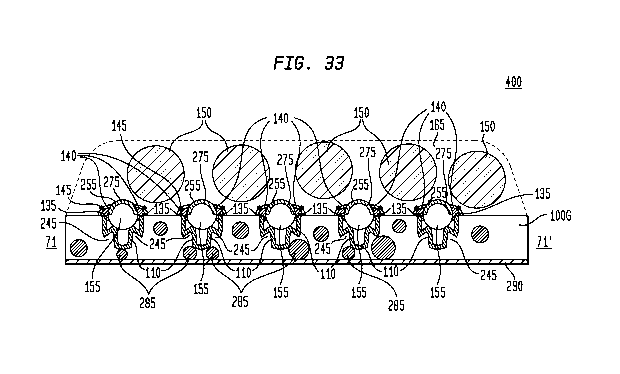
Figure (or "FIG.") 33 is a cross-sectional view of the sixth exemplary base
with a plurality of first conductors, a plurality of substantially spherical
diodes, a plurality of
insulators, a plurality of second conductors, a plurality of third conductors,
and a plurality of
lenses suspended in a polymer for an apparatus embodiment in accordance with
the teachings
of the present invention.
Figure (or "FIG.") 34 is a perspective view of an exemplary base with a first
conductor, a plurality of substantially spherical diodes, an insulator, a
second conductor, and a
third conductor for an apparatus embodiment in accordance with the teachings
of the present
invention.
Figure (or "FIG.") 35 is a perspective view of an exemplary base with a first
conductor, a plurality of substantially spherical diodes, an insulator, a
second conductor, a third
conductor, and a plurality of lenses suspended in a polymer for an apparatus
embodiment in
accordance with the teachings of the present invention.
Figure (or "FIG.") 36 is a cross-sectional view of the exemplary base with a
first conductor, a plurality of substantially spherical diodes, an insulator,
a second conductor, a
third conductor, and a plurality of lenses suspended in a polymer for an
apparatus embodiment
in accordance with the teachings of the present invention.
Figure (or "FIG.") 37 is a perspective view of a ninth exemplary base with a
first conductor, a first conductor (or conductive) adhesive layer, a plurality
of substrate
particles, and an insulator for an apparatus embodiment in accordance with the
teachings of the
present invention.
Figure (or "FIG.") 38 is a cross-sectional view of the ninth exemplary base
with a first conductor, a first conductor adhesive layer, a plurality of
substrate particles, and an
insulator for an apparatus embodiment in accordance with the teachings of the
present
invention.
Figure (or "FIG.") 39 is a perspective view of a ninth exemplary base with a
first conductor, a first conductor (or conductive) adhesive layer, a plurality
of diodes formed
using a deposited substrate (or semiconductor) layer or region over a
plurality of substrate
particles, an insulator, a second conductor, and a plurality of lenses
(suspended in a polymer
CA 02772919 2012-03-01
WO 2011/034908 PCT/US2010/048918
- 19-
(resin or other binder)) having been deposited for an exemplary apparatus
embodiment in
accordance with the teachings of the present invention.
Figure (or "FIG.") 40 is a cross-sectional view of the ninth exemplary base
with a first conductor, a first conductor (or conductive) adhesive layer, a
plurality of diodes
formed using a deposited substrate (or semiconductor) layer or region over a
plurality of
substrate particles, an insulator, a second conductor, and a plurality of
lenses (suspended in a
polymer (resin or other binder)) having been deposited for an exemplary
apparatus embodiment
in accordance with the teachings of the present invention.
Figure (or "FIG.") 41 is a block diagram illustrating a first system
embodiment
in accordance with the teachings of the present invention.
Figure (or "FIG.") 42 is a block diagram illustrating a second system
embodiment in accordance with the teachings of the present invention.
Figure (or "FIG.") 43 is a flow chart illustrating a method embodiment in
accordance with the teachings of the present invention.
DETAILED DESCRIPTION OF EXEMPLARY EMBODIMENTS
While the present invention is susceptible of embodiment in many different
forms, there are shown in the drawings and will be described herein in detail
specific
exemplary embodiments thereof, with the understanding that the present
disclosure is to be
considered as an exemplification of the principles of the invention and is not
intended to limit
the invention to the specific embodiments illustrated. In this respect, before
explaining at least
one embodiment consistent with the present invention in detail, it is to be
understood that the
invention is not limited in its application to the details of construction and
to the arrangements
of components set forth above and below, illustrated in the drawings, or as
described in the
examples. Methods and apparatuses consistent with the present invention are
capable of other
embodiments and of being practiced and carried out in various ways. Also, it
is to be
understood that the phraseology and terminology employed herein, as well as
the abstract
included below, are for the purposes of description and should not be regarded
as limiting.
For selected embodiments, the invention disclosed herein is related to United
States Patent Application Serial No. 11/756,616, filed May 31, 2007, inventors
William
Johnstone Ray et al., entitled "Method of Manufacturing Addressable and Static
Electronic
Displays" and to United States Patent Application Serial No. 11/756,619, filed
May 31, 2007,
inventors William Johnstone Ray et al., entitled "Addressable or Static Light
Emitting or
Electronic Apparatus" (the "related applications"), which are commonly
assigned herewith, the
CA 02772919 2012-03-01
WO 2011/034908 PCT/US2010/048918
-20-
contents of all of which are incorporated herein by reference in their
entireties, and with
priority claimed for all commonly disclosed subject matter.
FIG. 1 is a perspective view of an exemplary base 100, 100A, 100B, 1000,
100D for an apparatus embodiment in accordance with the teachings of the
present invention.
FIG. 2 is a cross-sectional view (through the 25-25' plane) of a first
exemplary base 100 for an
apparatus embodiment in accordance with the teachings of the present
invention. FIG. 3 is a
cross-sectional view (through the 25-25' plane) of a second exemplary base
100A for an
apparatus embodiment in accordance with the teachings of the present
invention. FIG. 4 is a
cross-sectional view (through the 25-25' plane) of a third exemplary base 100B
for an
apparatus embodiment in accordance with the teachings of the present
invention. FIG. 5 is a
cross-sectional view (through the 25-25' plane) of a fourth exemplary base
1000 for an
apparatus embodiment in accordance with the teachings of the present
invention. It should be
noted that in many of the various perspective or lateral views (such as FIGs.
1, 6, 11, 13, 16,
18, 21, 26, 28, 34, 35), any one or more corresponding bases 100 may be
utilized, with various
cross sections (such as FIGs. 2 - 5, 7, 8, 12, 14, 15, 17, 19, 20, 22, 27, 29)
considered particular
exemplary instances or instantiations when that corresponding base is utilized
as shown in a
corresponding perspective view. It also should be noted that any reference to
apparatus, such
as an apparatus 200, 300, 400, 500, 600 and/or 700, should be understood to
mean and include
its or their variants, and vice-versa, including apparatuses 200A, 200B, 300A,
300B, 400A,
400B, 500A, 500B, 600A, 600B, 700A, and 700B discussed below. In addition, it
should be
noted that apparatuses 200, 200A, 200B, 300, 300A, 300B, 400, 400A, 400B, 500,
500A,
500B, 600, 600A, 600B, 700A, and 700B may differ from one another concerning
any one or
more of the following, as discussed in greater detail below: (1) the existence
of and/or shape of
any cavities, channels or grooves 105 within their corresponding bases 100;
(2) the shape of the
substrate (or semiconductor) particles 120 and/or lenses 150; (3) having
single layers of
conductors and insulators, rather than pluralities; (4) inclusion of
integrally formed or other
conductive vias 280, 285; (5) inclusion of a backplane 290; (6) deposition
methods utilized to
create the corresponding apparatuses; etc. Further, apparatuses 200A, 300A,
400A, 500A,
600A, 700A, differ from apparatuses 200B, 300B, 400B, 500B, 600B, 700B insofar
as
incorporated diodes 155 are light emitting diodes for apparatuses 200A, 300A,
400A, 500A,
600A, 700A and photovoltaic diodes for apparatuses 200B, 300B, 400B, 500B,
600B, 700B,
also as discussed in greater detail below. Otherwise, any reference to any
feature or element of
any of an apparatus 200, 300, 400, 500, 600 and/or 700 should be understood to
be equally
applicable to any of the other apparatus 200, 300, 400, 500, 600 and/or 700
embodiments,
individually and/or with combinations of such features or elements, such that
any apparatus
CA 02772919 2012-03-01
WO 2011/034908 PCT/US2010/048918
-21-
200, 300, 400, 500, 600 and/or 700 may include or comprise any of the elements
of any of the
other apparatus 200, 300, 400, 500, 600 and/or 700 embodiments, in any
combination. In
addition, any and all of the various deposition, process and/or other
manufacturing steps are
applicable to any of the various apparatuses 200, 300, 400, 500, 600 and/or
700.
It should also be noted that the term "substrate" may utilized to refer to two
different components, a base (supporting or foundational substrate) 100
(including 100A -
100H) which forms a base or support for other components, and which may be
referred to
herein equivalently as a "substrate" in the related applications, such as for
printing various
layers on a substrate, and a plurality of substrate particles 120, such as a
plurality of
semiconductor, polymer, or organic light emitting or photovoltaic substrate
particles utilized to
form corresponding diodes 155. Those having skill in the art will recognize
that these various
substrates are different based upon both the context and the corresponding
reference numerals,
and to avoid confusion, a supporting- or foundational-type substrate will be
referred to herein
as a "base", with "substrate" utilized in the typical sense of the electronics
and/or
semiconductor art to mean and refer to the material comprising substrate
particles 120.
As illustrated in FIGs. 1 through 5, an exemplary base 100, 100A, 100B, 1000,
100D (and 100E - 100G discussed below) includes a plurality of cavities
(channels, trenches or
voids) 105, which for the selected embodiment, are formed as elongated
cavities, effectively
forming channels, grooves or slots (or, equivalently, depressions, valleys,
bores, openings,
gaps, orifices, hollows, slits, passages, or corrugations), which are
separated from each other by
a corresponding plurality of ridges (peaks, raised portions or crests) 115 of
the exemplary base
100, 100A - 100G. While the cavity, channel or groove 105 for bases 100, 100A,
100B, 1000,
100D is illustrated as curved (semi-circular or semi-elliptical) and extending
substantially
straight (in the direction perpendicular to the 25-25' plane), any and all
cavities, channels or
grooves 105 of any shape and/or size and extending in any one or more
directions are
considered equivalent and within the scope of the invention as claimed,
including without
limitation square, rectangular, curvilinear, wavy, irregular, differently
sized, etc., with
additional exemplary shapes of cavities, channels or grooves 105 illustrated
in other Figures
and discussed below. The plurality of cavities, channels or grooves 105 are
spaced-apart, and as
illustrated separated from each other by the ridges (peaks, raised portions or
crests) 115, and
will be utilized to shape and define a plurality of first conductors 110 for
selected
embodiments, as discussed below. While the cavities or channels 105 are
illustrated in FIG. 1
and other Figures as substantially parallel and oriented in substantially the
same direction, those
having skill in the art will recognize that innumerable variations are
available, including depth
and width of the channels, channel direction or orientation (e.g., circular,
elliptical, curvilinear,
CA 02772919 2012-03-01
WO 2011/034908 PCT/US2010/048918
-22-
wavy, sinusoidal, triangular, fanciful, artistic, irregular, etc.), spacing
variations, type of void or
cavity (e.g., channel, depression or bore), etc., and all such variations are
considered equivalent
and within the scope of the present invention. Bases 100 having additional
forms are also
illustrated and discussed below with reference to FIGs. 9, 10, 23-25, 30-33,
and 37-39. For
example, an exemplary base 1 OOH which has a substantially flat overall form
factor and is
without any significant surface variation (i.e., does not have any cavities,
channels or grooves
105) is illustrated and discussed below with reference to FIGs. 37 - 39.
A base 100, 100A, 100B, 1000, 100D (and the other bases 100E, 100F, 100G,
1 OOH discussed below) may be formed from or comprise any suitable material,
such as plastic,
paper, cardboard, or coated paper or cardboard, for example and without
limitation. In an
exemplary embodiment, a base 100 (including 100A, 100B, 1000, 100D, 100E, 100F
and/or
100G) comprises an embossed and coated paper or plastic having the plurality
of cavities 105
formed integrally therein, such as through a molding process, including an
embossed paper or
embossed paper board commercially available from Sappi, Ltd., for example.
Also in an
exemplary embodiment, base 100 (including 100A, 100B, 1000, 100D, 100E, 100F,
100G
and/or 1OOH) comprises a material having a dielectric constant capable of or
suitable for
providing substantial electrical insulation. A base 100, 100A, 100B, 1000,
100D, 100E, 100F,
100G, 100H may comprise, also for example, any one or more of the following:
paper, coated
paper, plastic coated paper, fiber paper, cardboard, poster paper, poster
board, books,
magazines, newspapers, wooden boards, plywood, and other paper or wood-based
products in
any selected form; plastic or polymer materials in any selected form (sheets,
film, boards, and
so on); natural and synthetic rubber materials and products in any selected
form; natural and
synthetic fabrics in any selected form; glass, ceramic, and other silicon or
silica-derived
materials and products, in any selected form; concrete (cured), stone, and
other building
materials and products; or any other product, currently existing or created in
the future. In a
first exemplary embodiment, a base 100, 100A, 100B, 1000, 100D, 100E, 100F,
100G, 100H
may be selected which provides a degree of electrical insulation (i.e., has a
dielectric constant
or insulating properties sufficient to provide electrical insulation of the
one or more first
conductors 110 deposited or applied on a first (front) side of the base 100
(including 100A,
100B, 1000, 100D, 100E, 100F, 100G and/or 100H), either electrical insulation
from each
other or from other apparatus or system components. For example, while
comparatively
expensive choices, a glass sheet or a silicon wafer also could be utilized as
a base 100, 100A,
100B, 1000, 100D, 100E, 100F, 100G, 100H. In other exemplary embodiments,
however, a
plastic sheet or a plastic-coated paper product is utilized to form the base
100, 100A, 100B,
1 000, 100D, 100E, 100F, 100G, 100H such as the patent stock and 100 lb. cover
stock
CA 02772919 2012-03-01
WO 2011/034908 PCT/US2010/048918
-23-
available from Sappi, Ltd., or similar coated papers from other paper
manufacturers such as
Mitsubishi Paper Mills, Mead, and other paper products. In additional
exemplary
embodiments, any type of base 100, 100A, 100B, 1000, 100D, 100E, 100F, 100G,
100H may
be utilized, including without limitation, those with additional sealing or
encapsulating layers
(such as plastic, lacquer and vinyl) deposited to one or more surfaces of the
base 100, 100A,
10013, 1000, 100D, 100E, 100F, 100G, 100H.
The exemplary bases 100 as illustrated in the various Figures have a form
factor which is substantially flat in an overall sense, such as comprising a
sheet of a selected
material (e.g., paper or plastic) which may be fed through a printing press,
for example and
without limitation, and which may have a topology on a first surface (or side)
which includes
cavities, channels or grooves 105 (e.g., reticulated, substantially flat bases
100, 100A, 100B,
1000, 100D, 100E, 100F, 100G) or having a first surface which is substantially
smooth
(substantially smooth and substantially flat base 1 OOH) within a
predetermined tolerance (and
does not include cavities, channels or grooves 105). Those having skill in the
art will recognize
that innumerable, additional shapes and surface topologies are available, are
considered
equivalent and within the scope of the claimed invention.
Referring to FIG. 3, a second exemplary base 100A further comprises two
additional components or features, any of which may be integrally formed as
part of second
exemplary base 100A, or which may be deposited over another material, such as
a base 100, to
form a second exemplary base 100A. As illustrated, the second exemplary base
100A further
comprises a reflector, refractor or mirror 250, such as an optical grating, a
Bragg reflector or
mirror, which may be covered by a coating 260, such as a substantially clear
plastic coating
(e.g., polyester, mylar, etc.), or having any suitable index of refraction,
such that the interior of
the cavities, channels or grooves 105 is substantially smooth (particularly
when the reflector,
refractor or mirror 250 may be implemented as a refractive grating, for
example). The
reflector, refractor or mirror 250 is utilized to reflect incident light
either back toward the
cavities, channels or grooves 105 (and any incorporated diodes 155, discussed
below, such as
for photovoltaic applications) or toward the (first) surface of an apparatus
(200, 300, 400, 500,
600 and/or 700) having the cavities, channels or grooves 105.
Referring to FIG. 4, a third exemplary base 100B further comprises a
reflective
coating 270, such as an aluminum or silver coated polyester or plastic, for
example, which may
be integrally formed as part of third exemplary base 100B, or which may be
deposited over
another material, such as a base 100, to form a third exemplary base 100B. The
reflective
coating 270 is also utilized to reflect incident light either back toward the
cavities, channels or
grooves 105 (and any incorporated diodes 155, discussed below, such as for
photovoltaic
CA 02772919 2012-03-01
WO 2011/034908 PCT/US2010/048918
-24-
applications) or toward the surface of the apparatus (200, 300, 400, 500, 600
and/or 700)
having the cavities, channels or grooves 105. The reflector, refractor or
mirror 250 or the
reflective coating 270 is generally selected to reflect or refract light at a
wavelength appropriate
for a selected bandgap of the plurality of diodes 155 discussed below,
depending upon the
selected application.
Referring to FIG. 5, a fourth exemplary base 1000 may include any of the
coatings and/or reflectors discussed above (250, 260, 270), and also further
comprises any of
two additional components or features, a plurality of conductive vias 280 and
a conductive
backplane 290, any of which may be integrally formed as part of fourth
exemplary base 1000,
or which may be deposited or applied over or within another material, such as
a base 100, to
form a fourth exemplary base 1000. For example, exemplary conductive vias 280
may be
formed by filling a corresponding void in the fourth exemplary base 1000 with
a conductive
ink or polymer, such as during deposition of the first plurality of conductors
110 discussed
below. Also for example, the conductive vias 280 may be integrally formed with
the fourth
exemplary base 1000, such as formed of metal, carbon or other conductive pins
or wires which
are embedded within a plastic sheet to form the fourth exemplary base 1000.
Another variation
of conductive vias (as distributed (randomly or regularly), substantially
spherical conductive
vias 285) is illustrated and discussed below with reference to FIGs. 10 and
33. Also for
example, there may be one or more conductive vias 280, 285 for each
corresponding first
conductor 110. As another example, a conductive backplane 290 may be formed
integrally
with the base 1000 or deposited over a base (100), such as by coating or
printing the second
(back) side or surface of the base 100 with a conductive ink or polymer, such
as the exemplary
conductive inks or polymers described below. As illustrated, either or both a
plurality of
conductive vias 280 (and/or conductive vias 285) and/or a conductive backplane
290 may be
formed from any conductive substance of any kind or type, such as a metal, a
conductive ink or
polymer, or various other conductive materials, such as carbon or carbon
nanotubes, including
any of the materials which may comprise the first, second and/or third
conductors (110, 140,
145, respectively) described below, for example and without limitation. The
conductive vias
280 (and/or conductive vias 285) are utilized to couple, connect, and
otherwise conduct to
and/or from the one or more first conductors 110 (discussed below). The
conductive backplane
290 provides a convenient electrical coupling or connection between the
conductive vias 280,
285 and other system (350, 375) components, and may also function as an
electrode, for
example, to apply a voltage or current to the apparatus 200, 300, 400, 500,
600, 700 or to
receive a voltage or current generated by the apparatus 200, 300, 400, 500,
600, 700. In other
exemplary embodiments, separate wires, leads or other connections may be
provided to each,
CA 02772919 2012-03-01
WO 2011/034908 PCT/US2010/048918
-25-
some or all of the vias 280, in lieu of or in addition to a conductive
backplane 290, such as for
different types of addressability, as discussed in greater below. (In other
exemplary
embodiments implemented without vias 280 (285) and/or a conductive backplane
290, other
types of contacts may be made to the plurality of first conductors 110, such
as from the sides or
edges of the apparatus 200, 300, 400, 500, 600, 700, as discussed below.)
Conductive vias 280
and/or a conductive backplane 290 may also be included within any of the other
bases 100,
100A, 100B, 100D, 100E, 100F, 100G, 100H, and all such variations are
considered equivalent
and within the scope of the claimed invention.
A fifth exemplary base 100D is discussed below with reference to FIG. 8, and
combines the various features of the second exemplary base 100A and the fourth
exemplary
base 1000. Additional sixth, seventh and eighth bases 100G, 100E and 100F are
also discussed
below, having different forms for cavities, channels or grooves 105, such as
semicircular
channels 105 with interior projections (or supports) 245, off-axis parabolic
(paraboloid) shaped
channels 105A, and substantially hemispherical cavities 105B, with a ninth
exemplary base
1 OOH with a first side or surface having a substantially smooth surface
topology without
cavities, channels or grooves 105.
The various cavities, channels or grooves 105 may have any type or kind of
spacing between or among them. For example, in an exemplary embodiment, pairs
of cavities,
channels or grooves 105 are spaced comparatively closer together, with a
comparatively larger
spacing between each such pair of cavities, channels or grooves 105, providing
corresponding
spacing for one or more first conductors 110 deposited within the cavities,
channels or grooves
105, as discussed in greater detail below.
In accordance with the claimed invention, one or more first conductors 110 are
then applied or deposited (on a first side or surface of the base 100) within
the corresponding
plurality of cavities, channels or grooves 105, or over all or part of the
first surface or side or
the base 100, such as through a printing process. FIG. 6 is a perspective view
of an exemplary
base 100, 100A, 100B, 1000, 100D with a plurality of first conductors 110 for
an apparatus
embodiment in accordance with the teachings of the present invention. FIG. 7
is a cross-
sectional view (through the 30-30' plane) of an exemplary base 100 with a
plurality of first
conductors 110 for an apparatus embodiment in accordance with the teachings of
the present
invention. FIG. 8 is a cross-sectional view (through the 30-30' plane) of a
exemplary base
100D with a plurality of first conductors 110 for an apparatus embodiment in
accordance with
the teachings of the present invention. As mentioned above, exemplary base
100D further
comprises cavities, channels or grooves 105 (which are illustrated in FIG. 8
as partially filled
CA 02772919 2012-03-01
WO 2011/034908 PCT/US2010/048918
-26-
with one or more first conductors 110), a reflector, refractor or mirror 250,
a coating 260, one
or more conductive vias 280 (or 285), and a conductive backplane 290.
In an exemplary method of manufacturing the exemplary apparatuses 200, 300,
400, 500, 600 and/or 700, a conductive ink, polymer, or other conductive
liquid or gel (such as
a silver (Ag) ink or polymer or a carbon nanotube ink or polymer) is deposited
on a base 100,
100A, 100B, 1000, 100D, 100E, 100F, 100G, 100H, such as through a printing or
other
deposition process, and may be subsequently cured or partially cured (such as
through an
ultraviolet (uv) curing process), to form the one or more first conductors 110
(and such
conductive inks or polymers also may be utilized to form any of the other
conductors, such as
the conductive vias 280, 285 or the conductive backplane 290). In another
exemplary
embodiment, the one or more first conductors 110, the conductive vias 280,
285, and/or the
conductive backplane 290 may be formed by sputtering, spin casting (or spin
coating), vapor
deposition, or electroplating of a conductive compound or element, such as a
metal (e.g.,
aluminum, copper, silver, gold, nickel). Combinations of different types of
conductors and/or
conductive compounds or materials (e.g., ink, polymer, elemental metal, etc.)
may also be
utilized to generate one or more composite first conductors 110. Multiple
layers and/or types
of metal or other conductive materials may be combined to form the one or more
first
conductors 110, the conductive vias 280, 285, and/or the conductive backplane
290, such as
first conductors 110 comprising gold plate over nickel, for example and
without limitation. In
various exemplary embodiments, a plurality of first conductors 110 are
deposited in
corresponding cavities, channels or grooves 105, and in other embodiments, a
first conductor
110 may be deposited as a single conductive sheet (FIGs. 34 - 40) or otherwise
attached (e.g., a
sheet of aluminum coupled to a base 100H). Also in various embodiments,
conductive inks or
polymers which may be utilized to form the plurality of first conductors 110
may not be cured
or may be only partially cured prior to deposition of a plurality of substrate
(or semiconductor)
particles 120, and then fully cured while in contact with the plurality of
substrate (or
semiconductor) particles 120, such as for creation of ohmic contacts with the
plurality of
substrate (or semiconductor) particles 120 as discussed below.
Other conductive inks or materials may also be utilized to form the first
conductors 110, conductive vias 280, 285, conductive backplane 290, second
conductors 140,
third conductors 145, and any other conductors discussed below, such as
copper, tin, aluminum,
gold, noble metals, carbon, carbon nanotube ("CNT"), or other organic or
inorganic conductive
polymers, inks, gels or other liquid or semi-solid materials. In addition, any
other printable or
coatable conductive substances may be utilized equivalently to form the first
conductors 110,
conductive vias 280, 285, conductive backplane 290, second conductors 140
and/or third
CA 02772919 2012-03-01
WO 2011/034908 PCT/US2010/048918
-27-
conductors 145, and exemplary conductive compounds include: (1) from
Conductive
Compounds (Londonberry, NH, USA), AG-500, AG-800 and AG-5 10 Silver conductive
inks,
which may also include an additional coating UV-10065 ultraviolet curable
dielectric (such as
part of a first dielectric layer 125); (2) from DuPont, 7102 Carbon Conductor
(if overprinting
5000 Ag), 7105 Carbon Conductor, 5000 Silver Conductor (also for bus 310, 315
of Figure 42
and any terminations), 7144 Carbon Conductor (with UV Encapsulants), 7152
Carbon
Conductor (with 7165 Encapsulant), and 9145 Silver Conductor (also for bus
310, 315 of
Figure 42 and any terminations); (3) from SunPoly, Inc., 128A Silver
conductive ink, 129A
Silver and Carbon Conductive Ink, 140A Conductive Ink, and 150A Silver
Conductive Ink; (4)
from Dow Corning, Inc., PI-2000 Series Highly Conductive Silver Ink; and (5)
from Henckel /
Emerson & Cumings, 725A. As discussed below, these compounds may also be
utilized to
form other conductors, including the plurality of second conductors 140 and
any other
conductive traces or connections. In addition, conductive inks and compounds
may be
available from a wide variety of other sources.
Conductive polymers which are substantially optically transmissive may also
be utilized to form the one or more first conductors 110, conductive vias 280,
285, conductive
backplane 290, and also the plurality of second conductors 140 and/or third
conductors 145.
For example, polyethylene-dioxithiophene may be utilized, such as the
polyethylene-
dioxithiophene commercially available under the trade name "Orgacon" from AGFA
Corp. of
Ridgefield Park, New Jersey, USA, in addition to any of the other transmissive
conductors
discussed below and their equivalents. Other conductive polymers, without
limitation, which
may be utilized equivalently include polyaniline and polypyrrole polymers, for
example. In
another exemplary embodiment, carbon nanotubes which have been suspended or
dispersed in
a polymerizable ionic liquid are utilized to form various conductors which are
substantially
optically transmissive or transparent, such as one or more second conductors
140.
Various textures may be provided for the one or more first conductors 110,
such as having a comparatively rough or spiky surface, to facilitate
subsequent forming of
ohmic contacts with a plurality of substrate particles 120 discussed below.
One or more first
conductors 110 may also be given a corona treatment prior to deposition of the
plurality of
substrate particles 120, which may tend to remove any oxides which may have
formed, and also
facilitate subsequent forming of ohmic contacts with the plurality of
substrate particles 120.
In an exemplary embodiment, an embossed base 100, 100A, 100B, 1000,
100D, 100E, 100F, 100G is utilized, such that the base 100, 100A, 100B, 1000,
100D, 100E,
100F, 100G has an alternating series of ridges forming (generally smooth)
peaks (crests) and
valleys (cavities, channels or grooves 105), generally having a substantially
parallel orientation
CA 02772919 2012-03-01
WO 2011/034908 PCT/US2010/048918
-28-
(as an example), respectively illustrated as raised (or non-channel) portions
or crests 115 and
cavities (e.g., channels) 105. Conductive inks, polymers or other conductors
may then be
deposited to remain in the embossed valleys, creating a plurality of first
conductors 110 which
are not only substantially parallel, but which also have a physical separation
from each other
determined by the ridges (peaks, raised portions or crests) 115 provided
through an embossing
process, for example. Indeed, when the conductive inks or polymers are
deposited to the
embossed valleys (cavities, channels or grooves 105), the corresponding first
plurality of
conductors 110 are also separated from each other by the embossed ridges
(peaks, raised
portions or crests) 115 of the base 100, creating both a physical separation
and electrical
insulation (insulated through a corresponding dielectric constant), in
addition to being spaced
apart. For example, conductive inks or polymers may be coated or otherwise
deposited to an
embossed base in its entirety, and then utilizing a "doctor blade", the
conductive inks or
polymers are removed from all of the peaks (crests or raised portions 115),
such as by scraping
the blade across the surface of the base 100, 100A, 100B, 1000, 100D, 100E,
100F, 100G
having a coating of a conductive ink, leaving the conductive inks or polymers
within the
cavities, channels or grooves 105 to form a first plurality of conductors 110
having a
substantially parallel orientation. The amount of conductive ink or polymer
remaining in the
cavities, channels or grooves 105 depends on the type of doctor blade and the
applied pressure.
Alternatively, conductive inks or polymers also may be deposited (using
negligible or zero
pressure) on the embossed peaks (crests or raised portions 115), such as by
tip printing, leaving
the conductive inks or polymers to form a plurality of conductors having a
substantially parallel
orientation, such as for forming the plurality of second conductors 140 or a
plurality of third
conductors 145. Such printing may be performed as a separate manufacturing
step discussed
below.
For example, a conductive ink may be coated or otherwise deposited in excess
over the entire or most of the first side or surface of the base 100, 100A,
100B, 1000, 100D,
100E, 100F, 100G, with the excess conductive ink subsequently removed using a
"doctor
blade" or other type of scraping as known in the printing arts, followed by uv
curing of the
conductive ink within the plurality of cavities, channels or grooves 105.
Using such a doctor
blade, the conductive ink within the plurality of cavities, channels or
grooves 105 is allowed to
remain in place, with the balance of the conductive ink (such as covering the
non-channel
portions of the base (crests or raised portions 115) being removed by the
scraping process, such
as due to contact from the doctor blade. Depending upon the type of printing,
including the
stiffness of the doctor blade and the applied pressure, the conductive ink may
form a meniscus
within each of the plurality of cavities, channels or grooves 105 or may bow
upward instead,
CA 02772919 2012-03-01
WO 2011/034908 PCT/US2010/048918
-29-
for example. Those having skill in the electronic or printing arts will
recognize innumerable
variations in the ways in which the plurality of first conductors 110 may be
formed, with all
such variations considered equivalent and within the scope of the present
invention. For
example, the one or more first conductors 110 may also be deposited through
sputtering or
vapor deposition, without limitation. In addition, for other various
embodiments, the first
conductor(s) 110 may be deposited as a single or continuous layer, such as
through coating,
printing, sputtering, or vapor deposition, such as for the exemplary
embodiments illustrated and
discussed below with reference to FIGs. 34 - 40.
As a consequence, as used herein, "deposition" means, refers to and includes
any and all printing, coating, rolling, spraying, layering, sputtering,
plating, spin casting (or
spin coating), vapor deposition, lamination, affixing and/or other deposition
processes, whether
impact or non-impact, currently known or developed in the future, and
"printing" means, refers
to and includes any and all printing, coating, rolling, spraying, layering,
spin coating,
lamination and/or affixing processes, whether impact or non-impact, currently
known or
developed in the future, including without limitation screen printing, inkjet
printing, electro-
optical printing, electroink printing, photoresist and other resist printing,
thermal printing, laser
jet printing, magnetic printing, pad printing, flexographic printing, hybrid
offset lithography,
Gravure and other intaglio printing, for example. All such processes are
considered deposition
processes herein, may be utilized equivalently, and are within the scope of
the present
invention. Also significant, the exemplary deposition or printing processes do
not require
significant manufacturing controls or restrictions. No specific temperatures
or pressures are
required. No clean room or filtered air is required beyond the standards of
known printing or
other deposition processes. For consistency, however, such as for proper
alignment
(registration) of the various successively deposited layers forming the
various embodiments,
relatively constant temperature (with a possible exception, discussed below)
and humidity may
be desirable. In addition, the various compounds utilized may be contained
within various
polymers, binders or other dispersion agents which may be heat-cured or dried,
air dried under
ambient conditions, or uv cured, for example, and all such variations are
within the scope of the
present invention.
A particular advantage of use of a base 100, 100A, 100B, 1000, 100D, 100E,
100F, 100G having a plurality of cavities 105 is that printing registration is
not required to be
exact, and a one-dimensional or relative registration may be sufficient for
the successive
applications of the different materials and layers forming the apparatus 200,
300, 400, 500, 600
and/or 700.
CA 02772919 2012-03-01
WO 2011/034908 PCT/US2010/048918
-30-
Depending upon the selected embodiment, the depth of the plurality of
cavities,
channels or grooves 105 may vary from comparatively deep (e.g., one-half or
more of the
diameter of a substrate (semiconductor) particle 120) to comparatively shallow
(e.g., less than
one-half of the diameter of a substrate (semiconductor) particle 120). In
addition, as previously
mentioned, a base (100H) may have a surface topology which is substantially
flat, smooth or
even, without a plurality of cavities, channels or grooves 105 integrally
formed therein, such as
for application of the one or more first conductors 110 as a unitary
conductive sheet or layer,
without being spaced apart or electrically insulated from each other. In other
exemplary
embodiments, a base may have a substantially flat, smooth or even surface,
without a plurality
of cavities, channels or grooves 105 integrally formed therein, and instead
having ridges (crests
or raised portions 115) or other forms of separation built or deposited onto
the base which in
turn form cavities, channels or grooves 105, or no ridges (crests or raised
portions 115).
It should also be noted, generally for any of the applications of various
compounds herein, such as through printing or other deposition, the surface
properties or
surface energies may also be controlled, such as through the use of resist
coatings or by
otherwise modifying the "wetability" of such a surface, for example, by
modifying the
hydrophilic, hydrophobic, or electrical (positive or negative charge)
characteristics, for
example, of surfaces such as the surface of the base 100 (including 100A,
100B, 1000, 100D,
100E, 100F, 100G and/or 100H), the surfaces of the various first, second
and/or third
conductors (110, 140, 145, respectively), and/or the surfaces of the plurality
of substrate
particles 120 discussed below. In conjunction with the characteristics of the
compound,
suspension, polymer or ink being deposited, such as the surface tension, the
deposited
compounds may be made to adhere to desired or selected locations, and
effectively repelled
from other areas or regions.
FIG. 9 is a cross-sectional view of a sixth exemplary base 100G with a
plurality of first conductors 110 for an apparatus embodiment in accordance
with the teachings
of the present invention. FIG. 10 is a cross-sectional view (through the 31 -
31' plane) of the
sixth exemplary base 100G with a plurality of first conductors 110 for an
apparatus
embodiment in accordance with the teachings of the present invention. The
sixth exemplary
base 100G differs from the other exemplary bases 100 - 100F insofar as the
sixth exemplary
base 100G also comprises a plurality of integrally formed projections or
supports (equivalently,
extensions, protrusions, protuberances, etc.) 245 and a plurality of
integrally formed conductive
vias 285 (as a variation of the vias 280). As illustrated, each of the
projections (or supports)
245 are continuous and extend as a solid, raised rail down the entire length
of the channel 105;
in other embodiments not separately illustrated, the projections (or supports)
245 may be
CA 02772919 2012-03-01
WO 2011/034908 PCT/US2010/048918
-31-
discrete and discontinuous, such as projections (or supports) 245 having the
shape of individual
horns or spikes which are spaced apart and located at intervals (regular or
irregular) down the
length of a channel 105, for example and without limitation. The projections
(or supports) 245
may have any suitable form, including being smooth and continuous or sharp and
discontinuous, with all such variations considered equivalent and within the
scope of the
claimed invention. In an exemplary embodiment, the projections (or supports)
245 are shaped
to allow them to be integrally formed as part of the base 100G, such as by a
casting or other
molding method, also for example and without limitation.
Also as illustrated, the plurality of first conductors 110 have been deposited
to
be conformal and track the shape of the channels 105 with a substantially
uniform thickness
(i.e., a substantially even coating substantially following the contour of the
first side (surface)
of the base 100G). In an exemplary embodiment, a conductor (such as a metal)
may be
deposited (at a comparatively low temperature), such as by sputtering, spin
casting (or spin
coating), coating, or vapor deposition, over the entire first surface (side)
of the base 100G,
followed by substantially removing any conductor on the ridges (peaks, raised
portions or
crests) 115, such as by grinding or sanding the ridges (peaks, raised portions
or crests) 115 of
the base 100G, leaving the plurality of first conductors 110 remaining within
the channels 105.
In another exemplary embodiment, a resist coating is deposited to the ridges
(peaks, raised
portions or crests) 115, and a conductor (such as a metal) may be deposited,
such as by
sputtering, spin casting (or spin coating), or vapor deposition, over the
entire first surface of the
base 100G, followed by substantially removing any conductor on the ridges
(peaks, raised
portions or crests) 115, such as by dissolving the resist or by lifting off
the conductor on the
resist over the ridges (peaks, raised portions or crests) 115, and dissolving
any remaining resist.
In this latter method, the conductor may be deposited directionally, so that
the deposited
conductor is discontinuous at the edges of the ridges (peaks, raised portions
or crests) 115,
enabling the conductor on the ridges (peaks, raised portions or crests) 115 to
be removed
without affecting the remaining conductor deposited within the channels 105.
When the
selected conductor is aluminum, the first conductors 110 are also
significantly reflective and
capable of functioning as a reflective or mirror coating, in addition to
providing conductance.
As discussed in greater detail below with reference to FIGs. 11, 12 and 33,
the
projections (or supports) 245 serve to elevate (or support) a plurality of
substrate particles 120
above the bottom or remaining portion of the channel 105. As the plurality of
substrate
particles 120 are suspended in a carrier (liquid or gel, for example) for
deposition within the
channels 105, the elevation by the projections 245 provides for physically
supporting and/or
separating the plurality of substrate particles 120 from the suspending
carrier (which at least
CA 02772919 2012-03-01
WO 2011/034908 PCT/US2010/048918
-32-
initially remains at the bottom of the channel 105 and/or which may be
dissipated or removed
(such as through evaporation)). The first conductors 110 (on the projections
245) then form
ohmic contacts with the supported and elevated substrate particles 120,
without interference (or
with diminished interference) from any suspending carrier (or polymers or
resins) which may
be remaining.
The plurality of integrally formed conductive vias 285, as illustrated, may
comprise any type of conductor or conductive medium, as previously discussed
and without
limitation, and may have any suitable shape or form. In an exemplary
embodiment, the
conductive vias 285 are formed as substantially spherical metal balls or other
conductive beads
or pellets, and incorporated into the base 100G as it is being formed, such as
during a molding
process. The plurality of conductive vias 285 may then be distributed randomly
(as illustrated),
or periodically or otherwise regularly, within the base 100G. As the base 100G
is being
formed, at least some of the plurality of integrally formed conductive vias
285 will make
physical contact with both a first conductor 110 and the conductive backplane
290, thereby
providing electrical coupling between the first conductors 110 and the
conductive backplane
290. For such an exemplary embodiment, a sufficient number of conductive vias
285 are
provided during fabrication, such that when randomly distributed within the
base 100G, every
first conductor 110 is in contact with at least one conductive via 285 which
also is in contact
with the conductive backplane 290. In other exemplary embodiments, the
conductive vias 285
are (non-randomly) distributed in predetermined locations, also so that every
first conductor
110 is in contact with at least one conductive via 285 which also is in
contact with the
conductive backplane 290.
FIG. 11 is a perspective view of an exemplary base 100, 100A, 100B, 1000,
100D with a plurality of first conductors 110 and a plurality of substrate
particles 120 for an
apparatus embodiment in accordance with the teachings of the present
invention. FIG. 12 is a
cross-sectional view (through the 40 - 40' plane) of the fifth exemplary base
100D with a
plurality of first conductors 110 and a plurality of substrate particles 120
for an apparatus
embodiment in accordance with the teachings of the present invention.
Following deposition of
the one or more first conductors 110, the material (such as a conductive ink
or polymer) may be
cured or partially cured, to form a solid or semi-solid. In other embodiments,
the one or more
first conductors 110 may remain in a liquid or partially-cured form and be
cured subsequently.
Following the deposition of the one or more first conductors 110, with any
such curing, partial
curing, or non-curing, a suspension of a plurality of substrate particles 120
is deposited over the
one or more first conductors 110 in the cavities, channels or grooves 105, and
(most) form an
ohmic contact 265 with a corresponding first conductor 110.
CA 02772919 2012-03-01
WO 2011/034908 PCT/US2010/048918
-33-
In many exemplary embodiments, the plurality of substrate particles 120 are
comprised of a semiconductor substrate, such as a p+ silicon or GaN substrate,
and so may be
referred to as a plurality of semiconductor particles 120. In other exemplary
embodiments, the
plurality of substrate particles 120 may comprise other organic, inorganic, or
polymeric
materials, such as compounds or mixtures suitable for creating organic or
polymer light
emitting diodes, as discussed below, and so also may be referred to as a
plurality of light
emitting substrate particles 120 or photovoltaic substrate particles 120. A
wide variety of
suitable types of substrates for use as substrate particles 120 are discussed
in greater detail
below. Accordingly, any reference herein to a plurality of substrate particles
120 or,
equivalently, a plurality of substrate (semiconductor) particles 120 should be
understood to
mean and include any organic or inorganic substrate in a particulate form of
some kind which is
suitable for use in light emitting, photovoltaic, or other electronic
applications of any kind,
currently known or developed in the future, with any and all such substrates
considered
equivalent and within the scope of the claimed invention.
The suspension of a plurality of substrate particles 120 may be deposited, for
example, through a printing or coating process, such as by printing within the
plurality of
cavities 105 having the plurality of first conductors 110, or by printing over
a first conductor
110 which has been deposited as a layer (FIGs. 34 - 40) or sheet. As
illustrated in FIGs. 37 -
40, a conductive adhesive 11 OA has been deposited prior to deposition of the
substrate particles
120, as another mechanism for bonding an created ohmic contacts between the
substrate
particles 120 and the one or more first conductors 110. Also for example, the
suspension of a
plurality of substrate particles 120 may be coated over the base 100, 100A,
100B, 1000, 100D,
100E, 100F, 100G, 1 OOH and plurality of first conductors 110, with any excess
removed using
a doctor blade or other scraping process, as previously described.
For example and without limitation, the plurality of substrate particles 120
may
be suspended in a liquid, semi-liquid or gel carrier using any evaporative or
volatile organic or
inorganic compound, such as water, an alcohol, an ether, etc., which may also
include an
adhesive component, such as a resin, and/or a surfactant or other flow aid. In
an exemplary
embodiment, for example and without limitation, the plurality of substrate
particles 120 are
suspended in deionized water as a carrier, with water soluble thickeners such
as methyl
cellulose, guar gum or fumed silica (such as Cabosil), may also utilize a
surfactant or flow aid
such as octanol, methanol, isopropanol, or deionized octanol or isopropanol,
and may also use a
binder such as an anisotropic conductive binder containing substantially or
comparatively small
nickel beads (e.g., 1 micron) (which provides conduction after compression and
curing (as
discussed below) and may serve to improve or enhance creation of ohmic contact
265, for
CA 02772919 2012-03-01
WO 2011/034908 PCT/US2010/048918
-34-
example), or any other uv, heat or air curable binder or polymer, including
those discussed in
greater detail below (and which also may be utilized with dielectric
compounds, lenses, and so
on). The volatile or evaporative components are dissipated, such as through a
heating, uv cure
or any drying process, for example, to leave the substrate particles 120
substantially or at least
partially in contact with and adhering to the one or more first conductors
110. The suspending
material may also include reflective, diffusing or scattering particles, for
example, to aid in
light transmission in a direction normal to a base 100, 100A, 100B, 1000,
100D, 100E, 100F,
100G, 1OOH for light emitting applications.
Additional steps or several step processes may also be utilized for deposition
of
the plurality of substrate particles 120 over the plurality of first
conductors 110 and within the
cavities, channels or grooves 105. Also for example and without limitation, a
binder such as a
methoxylated glycol ether acrylate monomer (which may also include a water
soluble
photoinitiator such TPO (triphosphene oxides)) or an anisotropic conductive
binder may be
deposited first, followed by deposition of the plurality of substrate
particles 120 which have
been suspended in any of the carriers discussed above.
For example, when the plurality of first conductors 110 have only been cured
partially or are uncured when the plurality of substrate particles 120 are
deposited, the plurality
of substrate particles 120 may become slightly or partially embedded within
the plurality of
first conductors 110, helping to form an ohmic contact 265, as illustrated in
the various Figures.
Additional embedding or contact creation may also occur through an application
of pressure (as
discussed below with reference to FIG. 13), thermal (heat) processing, uv
curing, etc.
In an exemplary embodiment, the suspending medium for the plurality of
substrate particles 120 also comprises a dissolving or other reactive agent,
which initially
dissolves or re-wets some of the one or more first conductors 110. When the
suspension of the
plurality of substrate particles 120 is deposited and the surfaces of the one
or more first
conductors 110 then become partially dissolved or uncured, the plurality of
substrate particles
120 may become slightly or partially embedded within the one or more first
conductors 110,
also helping to form an ohmic contact 265, and creating a "chemical bonding"
or "chemical
coupling" between the plurality of substrate particles 120 and the one or more
first conductors
110. As the dissolving or reactive agent dissipates, such as through
evaporation, the plurality
of first conductors 110 re-hardens (or re-cures) in substantial contact with
the plurality of
substrate particles 120. An exemplary dissolving or reactive agent, for
example and without
limitation, is proplyene glycol monomethyl ether acetate (C6H1203) (sold by
Eastman under the
name "PM Acetate"), used in an approximately 1:8 molar ratio (or 22:78 by
weight) with
isopropyl alcohol (or isopropanol) to form the suspending medium for the
plurality of substrate
CA 02772919 2012-03-01
WO 2011/034908 PCT/US2010/048918
-35-
particles 120. Other exemplary dissolving or reactive agents, also for example
and without
limitation, include a variety of dibasic esters, and mixtures thereof, such as
dimethyl succinate,
dimethyl adipate and dimethyl glutarate (which are available in varying
mixtures from Invista
under the product names DBE, DBE-2, DBE-3, DBE-4, DBE-5, DBE-6, DBE-9 and DBE-
113).
In an exemplary embodiment, DBE-9 in an approximately 1:10 molar ratio with
isopropanol
also has been utilized.
The plurality of substrate particles 120 may be comprised of any type of
semiconductor element, material or compound, such as silicon, gallium arsenide
(GaAs),
gallium nitride (GaN), or any inorganic or organic semiconductor material, and
in any form,
including GaP, InAlGaP, InAlGaP, AlInGaAs, InGaNAs, AlInGASb, for example and
without
limitation. For example, to form semiconductor substrate particles 120,
silicon may be utilized
as a monocrystal, as polysilicon, amorphous silicon, and so on, and does not
require the
epitaxial crystal growth of semiconductor integrated circuits and conventional
diodes, with a
similar variety of crystal structures and amorphous forms also available for
gallium arsenide,
gallium nitride, and other semiconductor compounds. The plurality of substrate
particles 120
also may be comprised of any type of organic or inorganic compound or polymer
utilized for
light emission or energy absorption (photovoltaics), such as the various
polymers and
compounds utilized for light emitting diodes ("OLEDs"), phosphorescent OLEDs
("PHOLEDs"), polymer light emitting diodes ("PLEDs"), light emitting polymers
("LEPs"),
including for example and without limitation polyacetylene compounds,
polypyrrole
compounds, polyaniline compounds, poly(p-phenylene vinylene), polyfluorene,
conjugated
dendrimers, organo-metallic chelates (e.g., Alg3), and any and all of their
corresponding
derivatives, substituted side chains, etc., which also may have encapsulated
forms, such as
encapsulated in a micelle or other container. As mentioned above, "substrate
particles" may
include any inorganic or organic semiconductor, energy emitting, energy
absorbing, light
emitting, photovoltaic, or other electronic material, and any and all such
elements, compounds,
mixtures and/or suspensions are within the scope of the claimed invention.
In FIGs. 11 - 24 and 32 - 40, the substrate particles 120 are illustrated as
being
substantially spherical. In addition, while the substrate particles 120 (and
diodes 155 and
lenses 150) are or may be referred to as "spherical" for one or more exemplary
embodiments, it
should be understood that as used herein, "spherical" means and includes
"substantially
spherical", i.e., substantially or mostly spherical to the extent of being
within a predetermined
or other selected variance, tolerance or other specification, as virtually no
actual object is
perfectly spherical in a theoretical or textbook sense. For example and
without limitation, the
various spherical particles (substrate particles, diodes, lenses) utilized in
the exemplary
CA 02772919 2012-03-01
WO 2011/034908 PCT/US2010/048918
-36-
embodiments typically will lack at least some uniformity (1) within each such
sphere (i.e., there
will be some variation in its radius from the center to different points of
the surface, and will be
slightly aspherical to some degree), (2) from sphere to sphere, with
variations in sizes of
spheres, (3) in the various shapes and sizes of particles, with some or many
being substantially
spherical (and others significantly aspherical and/or misshapen, depending
upon the tolerances
of the supplier, for example), and (4) in surface properties, with substrate
particles 120 having
substantially smooth or polished surfaces and others having more surface
variation or
roughness. The substrate particles 120 may be formed as spherical particles,
beads or pellets as
known or becomes known in the art, such as disclosed for silicon
(semiconductor) particles in
Hamakawa et al. U.S. Patent No. 6,706,959, issued March 16, 2004, entitled
"Photovoltaic
Apparatus and Mass-Producing Apparatus for Mass-Producing Spherical
Semiconductor
Particles", which is incorporated by reference herein with the same full force
and effect as if set
forth in its entirety herein. Other aspherical or otherwise irregular
substrate particles may be
formed into substantially spherical substrate particles through any of various
types of polishing
methods, such as in a ball mill, for example and without limitation.
In various exemplary embodiments, the plurality of substrate particles 120 are
subsequently converted in situ into corresponding diodes 155, as discussed in
greater detail
below. Accordingly, the plurality of substrate particles 120 are sized to
provide one or more
selected sizes of the resulting plurality of diodes 155, such as resulting
diodes 155 in the range
of about 10-40 microns ( m), for example, which is considerably smaller (by
orders of
magnitude) than prior art light emitting or photovoltaic diodes. In another
exemplary
embodiment, the diodes 155 are in the range of about 25-40 microns ( m), also
for example
and without limitation. Use of such small substrate and diode sizes are
possible due to the
novel methods of manufacturing herein, including the use of suspensions of the
plurality of
substrate particles 120 and the use of deposition techniques such as printing,
which allow
handling of the substrate particles as a group, en masse, rather than
requiring individual
placement of each particle 120. In addition, also as discussed in greater
detail below, the very
small size of the resulting diodes 155 is especially advantageous, providing
an increased
amount of a (pn) junction per amount of substrate material, enabling higher
efficiencies of light
output (for LED applications) or conversion of light into electrical energy
(for photovoltaic
applications).
In various exemplary embodiments, the plurality of substrate particles 120 are
selected or designed to have a shape which facilitates or creates optical
resonance at one or
more selected frequencies, such as substantially spherical, substantially
toroidal (or ring)
shaped, cylindrical or rod shaped, etc., and which are referred to
individually and collectively
CA 02772919 2012-03-01
WO 2011/034908 PCT/US2010/048918
-37-
herein as substantially optically "resonant" diodes 155 and/or semiconductor
or substrate
particles 120. In addition, a plurality of substrate particles 120 may also be
selected or
designed to have a shape which may facilitate mode coupling with the plurality
of lenses 150,
as discussed in greater detail below.
In other exemplary embodiments, the plurality of substrate particles 120 may
have other shapes and forms, such as faceted, oblong (elliptical),
substantially rectangular,
substantially flat, or substantially irregular or aspherical, as illustrated
in FIGs. 26 - 31, for
example and without limitation. For example, faceted substrate particles 120
may be useful for
light emission. Also for example, a substantially rectangular or substantially
flat substrate
particles 120, such as the shape and size of a prior art, conventional diode,
may also be utilized
in selected exemplary embodiments. In addition, the plurality of substrate
particles 120 may
have any of myriad sizes and shapes, with a variety of sizes utilized, such as
to provide
emission, absorption or optical resonance at a plurality of wavelengths of
light or other
electromagnetic (EM) waves. For example and without limitation, in an
exemplary
embodiment, the substrate particles 120 are substantially spherical (within a
predetermined
tolerance) and in a range of about 10-40 microns, and potentially in the range
of about 25-40 or
25-30 microns. In an exemplary embodiment, silicon, GaAs or GaN is utilized
which has been
doped (e.g., with Boron or another element) to be a p or p+ (equivalently
referred to as P or P+)
semiconductor, to facilitate forming corresponding ohmic contacts with the one
or more first
conductors 110. In other embodiments, n or n+ (equivalently referred to as N
or N+) dopant
levels also may be utilized.
Of special interest, it should be noted that other than suspending them into a
carrier (a suspending medium), the plurality of substrate particles 120 do not
require any
processing prior to depositing them over the one or more first conductors 110
in the plurality of
cavities, channels or grooves 105. For example, the plurality of substrate
particles 120 do not
require any micromachining to change their shape or to expose interior
portions, in sharp
contrast to the prior art.
In addition, at this point in the process of creating an apparatus (200, 300,
400,
500, 600 and/or 700), the plurality of substrate particles 120 are
substantially isotropic and do
not have and do not require any orientation during or prior to depositing them
over the one or
more first conductors 110 (in the plurality of cavities, channels or grooves
105). Rather, also in
sharp contrast with the prior art, an orientation or difference in the
substrate (e.g.,
semiconductor) material is created subsequently when the plurality of
substrate particles 120
are formed into diodes in situ, with the subsequent formation of a
corresponding pn (or
equivalent) junction in a substrate (e.g., semiconductor) particle 120 which
has already been
CA 02772919 2012-03-01
WO 2011/034908 PCT/US2010/048918
-38-
fixed in place during the manufacturing and creation of an apparatus 200, 300,
400, 500, 600,
700
As an option, provided sufficient ohmic contacts may be created between the
plurality of substrate particles 120 and the one or more first conductors 110,
the carrier or
suspending material for the plurality of substrate particles 120 may also
include an insulating
(or dielectric) binder or other polymer, which may be comprised of any curable
compound
having a reasonably high dielectric constant sufficient to provide electrical
insulation between
the plurality of first conductors 110 and the plurality of second conductors
140 discussed
below. As discussed in greater detail below, a wide variety of dielectric
compounds may be
utilized, any and all or which are within the scope of the present invention,
and may be
included within air, heat- or uv-curable binders or other polymers, for
example, to form part or
all of the suspending liquid, semi-liquid or gel carrier.
Those having skill in the art will also recognize that various removable or
etchable compounds may also be utilized. For example, once the plurality of
substrate particles
120 have been embedded within or make sufficient electrical contact with the
plurality of first
conductors 110, followed by curing, all or part of the suspending material or
binder may be
removed, such as through an acid or ion etching process. Such an etching or
washing process
may also facilitate providing additional electrical contacts with the
plurality of semiconductor
spherical particles 120, such as the subsequent formation of electrical
contacts with the one or
more second conductors 140.
In another variation, the substrate particles 120 are suspended in a carrier
such
as an organic or inorganic solvent. The carrier is then allowed to evaporate,
such as through the
application of heat, air, or other methods to facilitate evaporation, and the
plurality of substrate
particles 120 are bonded to the one or more first conductors 110, such as
through use of a
dissolving or reactive agent (as discussed above), pressure, laser, uv or
thermal annealing or
alloying, or another application of energy in some form. Accordingly,
electrical coupling
between the plurality of substrate particles 120 and the one or more first
conductors 110 may
occur in any of a plurality of ways, any and all of which are within the scope
of the claimed
invention. For example and without limitation, such coupling may occur by
abutment,
pressure, laser, uv or thermal annealing or alloying, by partially embedding
the plurality of
substrate particles 120 within one or more first conductors 110 (such as when
the conductive
ink or polymer forming the one or more first conductors 110 was uncured or
only partially
cured prior to depositing the plurality of substrate particles 120, or has
been dissolved or re-
wetted using a reactive suspending agent during the substrate particle
deposition process), or by
using anisotropic conductive polymers, which create an electrical connection
following
CA 02772919 2012-03-01
WO 2011/034908 PCT/US2010/048918
-39-
compression and curing, for example and without limitation. In an exemplary
embodiment, the
substrate particles 120 are annealed with or to one or more aluminum-based
first conductors
110 through thermal annealing between about 350 - 450 degrees C or any lower
temperature
sufficient for forming a desired or selected degree of ohmic contact(s)
without adversely
affecting other parts of the device, such as depending upon the composition of
the base 100.
FIG. 13 is a lateral view of the fifth exemplary base 100D with the plurality
of
substrate particles 120 passing through compressive rollers 195 for an
optional step in an
exemplary method of forming an apparatus embodiment in accordance with the
teachings of the
present invention. In such an exemplary embodiment, the plurality of first
conductors 110 may
remain in a liquid, gel, or partially-cured form. Following deposition of the
plurality of
substrate particles 120, the plurality of substrate particles 120 may be
pressed into the uncured
or partially cured plurality of first conductors 110, such as by moving the
base 100, 100A,
100B, 1000, 100D, 100E, 100F, 100G and/or 100H having the plurality of first
conductors 110
and the plurality of substrate particles 120 through such compressive rollers
195, or any other
means of applying pressure to or seating the plurality of substrate particles
120 in or against the
plurality of first conductors 110 to help form an ohmic contact (265) between
a semiconductor
particle 120 and a first conductor 110.
FIG. 14 is a cross-sectional view (through the 40 - 40' plane) of the fifth
exemplary base 100D with a plurality of first conductors 110 and a plurality
of substrate
particles 120 having a junction 275 formed therein and thereby comprising
diodes 155 for an
apparatus embodiment in accordance with the teachings of the present
invention. For
semiconductor substrate particles 120, the junction 275 is generally a pn (or
PN) junction 275,
while for organic or polymer substrate particles 120, the junction 275 may be
considered a
junction between the organic or polymer layers utilized to create OLEDs or
PLEDs, for
example and without limitation. As an example, for a plurality of substrate
particles 120
comprising a semiconductor having a first majority carrier (e.g., p+ or n+), a
layer or region
255 is created which has a second majority carrier (e.g., correspondingly n+
or p+), forming
junction 275. As part of a printing process, for a p or p+ semiconductor
substrate type, an n-
type dopant, such as a phosphorus or phosphorous and silicon in a carrier or
binder, is
deposited in a liquid, semi-liquid, gel, or film form, such as an ink or
polymer, to a first or
upper portion of the plurality of substrate particles 120, and heated, or
subject to laser energy,
or subject to another form of curing, annealing or alloying, such that the n-
type dopant or n-
type material diffuses into or bonds with the upper portion of the plurality
of substrate particles
120 to a sufficient degree, forming a penetration layer or region 255 which,
in this case, is an n-
type penetration layer or region 255 which defines a corresponding junction
275 (in this case, a
CA 02772919 2012-03-01
WO 2011/034908 PCT/US2010/048918
-40-
pn junction 275) with a p-type semiconductor substrate particle 120. In an
exemplary
embodiment, the (n-type) penetration layer or region 255 (and corresponding pn
junction 275)
is substantially curved and shell-shaped, such as hemispherical shell-shaped
when the plurality
of substrate particles 120 are substantially spherical, with the n-type layer
255 (and
corresponding pn junction 275) typically extending slightly below the level of
the outer coating
260, and is in sharp contrast to typical prior art diodes having a
substantially planar and flat pn
junction or a substantially planar and flat pn junction within a well of a
semiconductor
substrate. Conversely, a p-type penetration layer or region 255 may be formed
within an n-type
semiconductor particle 120, and is considered equivalent and also within the
scope of the
present invention. Also in an exemplary embodiment, an n-type dopant, such as
a phosphorus,
is suspended in a comparatively volatile carrier or binder which then
dissipates upon the
application of laser energy. A rapid laser pulse is utilized, or heat applied
(such as with a
tungsten heating element or bar or uv lamps, at 800-1200 degrees C for a
period of time which
may be a few tenths of a second up to 15-30 minutes,) on the first or top
portion of the plurality
of substrate particles 120, such that any heat dissipates quickly without
adversely affecting
other portions of the device. In exemplary embodiments, a resist may also be
utilized, such that
the remaining portions of the apparatus are not exposed to the deposited
dopant material or the
deposited dopant material does not adhere to those regions. In addition,
various surface
characteristics (such as wetting) may also be adjusted, as discussed above.
In another exemplary embodiment, various "spin-on" materials may be
deposited, through spinning, spraying or printing, to provide such n-type
doping. For such an
embodiment, a film of phosphorus, arsenic, or antimony doped glass, for
example and without
limitation, is deposited on the surface of the plurality of substrate
particles 120, such as silicon
particles, and heated, either forming an additional layer over (and a pn
junction at the interface
with) the substrate particles 120 (as illustrated in FIG. 15), or causing
diffusion to occur from
this film into the plurality of semiconductor (silicon) particles 120.
Exemplary n-type dopants
or spin-on materials include, for example and without limitation, dopants
available from the
Emulsitone Company of Whippany, New Jersey, USA, such as Emulsitone Emitter
Diffusion
Source N-250, Arsenosilicafilm and Antimonysilicafilm for buried layers,
Phosphorosilicafilm
5 x 10²⁰, and Phosphorofilm for solar cells. These exemplary dopants or spin-
on materials are
deposited, and depending on the application and dopants, such as for
Emulsitone Emitter
Diffusion Source N-250, may be initially heated to 150-200 degrees C for 15
minutes to harden
the film, followed by heating at 800-1200 degrees C for 15-30 minutes or any
lower
temperature capable of forming a junction 275 and/or layer or region 255
degree with the
desired or selected characteristics (such as a desired penetration depth) and
without adversely
CA 02772919 2012-03-01
WO 2011/034908 PCT/US2010/048918
-41-
affecting other parts of the device at that point in its manufacture, such as
temperatures as low
as or lower than 200 - 300 degrees C.
FIG. 15 is a cross-sectional view of a fifth exemplary base 100D with a
plurality of first conductors 110 and a plurality of substrate particles 120
following deposition
of a layer or region 255A, which also forms a junction 275, and thereby
comprising diodes 155
for an apparatus embodiment in accordance with the teachings of the present
invention, and
serves to illustrate another variation for the manufacture of diodes 155 in
situ, also in
accordance with the teachings of the present invention. For such an exemplary
embodiment, a
diode 155 comprises a layer or region 255A coupled to a substrate particle 120
to form a
junction 275. (FIG. 15 may also be considered a variation of a cross-sectional
view (through
the 40 - 40' plane) of FIG. 12, following deposition of one or more insulators
135 and a layer
or region 255A, which is not separately illustrated in a perspective view.
FIG. 15 may also be
considered a variation of a cross-sectional view (through the 50 - 50' plane)
of FIG. 16,
following deposition of a layer or region 255A, which also is not separately
illustrated in a
perspective view.)
As discussed in greater detail below with reference to FIGs. 16 and 17, one or
more insulators (or insulating layers) 135 may be deposited, to provide
electrical isolation
between one or more second conductors 140 and one or more first conductors
110. For this
exemplary embodiment, following deposition of the plurality of substrate
particles 120, one or
more insulators (or insulating layers) 135 may be deposited, followed by
deposition of a layer
or region 255A. In other exemplary embodiments, the one or more insulators (or
insulating
layers) 135 may be deposited after the in situ creation of diodes 155, as
discussed below.
Also as an example, for a plurality of substrate particles 120 comprising a
semiconductor having a first majority carrier (e.g., p+ or n+), a layer or
region 255A is created
which has a second majority carrier (e.g., correspondingly n+ or p+), also
forming junction
275. For semiconductor substrate particles 120, the junction 275 is generally
a pn (or PN)
junction 275, while for organic or polymer substrate particles 120, the
junction 275 may be
considered a junction between the organic or polymer layers utilized to create
OLEDs or
PLEDs, for example and without limitation. As part of a deposition process,
such as using
plasma deposition or sputtering, for semiconductor substrate type having a
first majority carrier
(e.g. p+ silicon), a semiconductor material having a second majority carrier
(e.g., an n-type
dopant, such as a phosphorus-doped silicon) is deposited over (on top of) a
first or upper
portion of the plurality of substrate particles 120 and any one or more
insulators 135. In
addition, in various embodiments, the semiconductor material having a second
majority carrier
may be deposited over the first surface (or side), covering a first or upper
portion of the
CA 02772919 2012-03-01
WO 2011/034908 PCT/US2010/048918
-42-
plurality of substrate particles 120, one or more insulators 135, and ridges
or crests 115
(illustrated as region 277). The corresponding deposited second majority
carrier (n-type)
semiconductor material forms a continuous semiconductor body with each of the
substrate
particles 120, such as forming a continuous crystal or other bond with the
upper portion of a
substrate particle 120, forming a deposited layer or region 255A which, in
this case, is an n-
type layer or region 255A which defines a corresponding junction 275 (in this
case, a pn
junction 275) with a first majority carrier (p-type) semiconductor substrate
particle 120. In an
exemplary embodiment, the (n-type) layer or region 255A (and corresponding pn
junction 275)
is formed as a "cap" over the substrate particle 120, and is also
substantially curved and shell-
shaped, such as hemispherical shell-shaped when the plurality of substrate
particles 120 are
substantially spherical, and also is in sharp contrast to typical prior art
diodes having a
substantially planar and flat pn junction or a substantially planar and flat
pn junction within a
well of a semiconductor substrate. In another embodiment, when the second
majority carrier
(n-type) semiconductor material is deposited as a layer which also covers the
insulators 135 and
ridges 115, the junction 275 is also formed as a "cap" at the interface with
the substrate particle
120, and is also substantially curved and shell-shaped, such as hemispherical
shell-shaped when
the plurality of substrate particles 120 are substantially spherical.
Conversely, a first majority
carrier (p-type) layer or region 255A may be formed over a second majority
carrier (n-type)
semiconductor particle 120, and is considered equivalent and also within the
scope of the
present invention. Following deposition of one or more insulators 135 and
formation of layers
or regions 255A, one or more second conductors 140 and other features and
elements may be
deposited as discussed below (beginning with FIG. 18 and following). An
exemplary apparatus
700 embodiment created using this methodology is illustrated and discussed
below with
reference to FIGs. 37 - 40.
In an exemplary embodiment, a layer or region 255A may be deposited using a
plasma deposition process, such as using a vacuum chamber having a few Torrs,
which may be
process chamber that is a module of an overall printing process, for example
and without
limitation. After deposition of one or more insulators 135 (described in
greater detail below),
the first side or surface may be treated, such as with a gas containing
fluorine, which may
slightly etch the plurality of substrate particles 120 when comprised of a
semiconductor such as
a doped silicon, and which may further create a surface of the insulators 135
which has
comparatively poor adhesion characteristics (e.g., Teflon-like). The plasma
deposition process
then deposits the semiconductor material, such as silicon, which adheres to
the first majority
carrier substrate particles 120, but does not substantially adhere to the
fluorinated surface of the
insulators 135 (and can be removed subsequently), and deposits the second
majority carrier (n-
CA 02772919 2012-03-01
WO 2011/034908 PCT/US2010/048918
-43-
type), which becomes incorporated into the deposited semiconductor material
and may also
further diffuse into the substrate particles 120, forming layer or region
255A. The deposited,
second majority carrier (n-type) doped semiconductor material is then in
intimate contact with
the substrate particles 120 having the first majority carrier, forming a
continuous semiconductor
(e.g., silicon) body having a junction 275, such as a n+p junction.
In another exemplary embodiment, a layer or region 255A may be deposited
using a sputtering process. After deposition of one or more insulators 135
(described in greater
detail below), the first side or surface may be cleaned or treated, such as
using a back sputtering
process. The sputtering process then deposits the semiconductor material doped
with a second
majority carrier, such as phosphorus-doped silicon from an n+ silicon source,
which adheres to
the first majority carrier substrate particles 120, the insulators 135, and
ridges 115, with the
second majority carrier (e.g., n-type) incorporated into the deposited
semiconductor material,
forming layer or region 255A. The deposited, second majority carrier (n-type)
doped
semiconductor material is then in intimate contact with the substrate
particles 120 having the
first majority carrier, forming a continuous semiconductor (e.g., silicon)
body having a junction
275, such as a n+p junction.
In exemplary embodiments, for both the plasma deposition and sputter
processes, a resist may also be utilized, such that the remaining portions of
the apparatus are
not exposed to the deposited dopant material or the deposited dopant material
does not adhere
to those regions. In addition, various surface characteristics (such as
wetting) may also be
adjusted, as discussed above.
Referring to both FIGs. 14 and 15, in various or selected exemplary
embodiments, the (pn) junction 275 may encompass varying percentages of a
shell region about
the plurality of substrate particles 120. For example, using percentages based
upon the amount
of surface area covered by a penetration layer or region 255 forming a
corresponding junction
275, when the plurality of substrate particles 120 are substantially
spherical, each substantially
hemispherical, shell-shaped (pn) junction 275 may encompass 15-60 percent of a
semiconductor particle 120; in other exemplary embodiments, a shell-shaped pn
junction 275
may encompass 15-55 percent of a semiconductor particle 120; and in various
exemplary
embodiments of substantially spherical substrate particles 120, may encompass
about or
approximately 20-50 percent, or 30-40 percent (plus or minus some small
percentage (A)) of a
semiconductor particle 120. This is also in sharp contrast to the prior art,
in which the (pn)
junction initially covers the entire spherical semiconductor, which
subsequently requires
micromachining to expose one of the substrate types. For example, in an
exemplary
embodiment, about 15 percent to 55 percent of each diode surface and
corresponding
CA 02772919 2012-03-01
WO 2011/034908 PCT/US2010/048918
-44-
penetration or diffusion region (255, 255A) of substantially all of the
plurality of substantially
spherical diodes has a second majority carrier (second dopant type) (n-type or
p-type) (i.e. has
the second dopant type over part, most or all of a first, primarily upper
surface of each diode
155, with the potential for some additional diffusion of the second dopant
type to the second,
lower surface of the diode), and the remaining diode surface and interior has
a first majority
carrier (or first dopant type) (p-type or n-type) (i.e., most, part or all of
a second, lower surface
of each diode comprises the original substrate that has not been covered by
the deposited
second dopant type and corresponding diffusion), with a pn junction formed
correspondingly
within each such substantially spherical diodes.
Because the (n-type) penetration layer or region 255 does not fully encompass
the semiconductor substrate particle 120, no further processing is needed to
expose a p-type
region, also in contrast with the prior art. Accordingly, ohmic contacts with
a p-type (or n-
type) region may be made directly on the unaltered, non-recessed, exterior of
the
semiconductor substrate particle 120, without any need for micromachining and
exposing an
interior, recessed portion. In addition, because the resulting diode 155 has
been created in situ,
no alignment of the pn junction and no placement of an oriented diode is
required, with proper
alignment and placement occurring automatically due to the novel method of
manufacturing a
diode 155 in place within an exemplary apparatus 200, 300, 400, 500, 600
and/or 700.
Furthermore, ohmic contacts between the substrate particles 120 and the one or
more first
conductors 110 have been created prior to diode 155 formation, also in sharp
contrast to typical
semiconductor fabrication techniques. Accordingly, a junction 275 has been
created in a diode
155 which is substantially curved and shell-shaped (and, for exemplary
embodiments,
substantially hemispherically shell-shaped or cap-shaped), and further
simultaneously or
concurrently having an "exposed" semiconductor substrate (e.g., a p-type
region bonded or
available for bonding to a conductor) and, for exemplary embodiments, an
exposed and
substantially hemispherically-shaped semiconductor substrate, which at least
in part has already
been coupled to one or more first conductors 110. Stated another way, a (pn)
junction 275 has
been created which is substantially curved and shell or cap-shaped (which
covers a
predetermined percentage of the semiconductor substrate particle 120 and which
does not, at
any time, encompass an entire semiconductor substrate particle 120), in a
semiconductor
substrate particle 120 which has already been bonded, attached or otherwise
coupled to a
conductor such as a first conductor 110.
Following diode 155 creation (with either a region or layer 255 or 255A), a
passivating or passivation layer may be formed, such as using a plasma
deposition process,
CA 02772919 2012-03-01
WO 2011/034908 PCT/US2010/048918
-45-
creating a comparatively tough and durable coating on the diodes 155, which in
various
embodiments, may also be flexible. For example, plasma deposition may be
utilized to
In various exemplary embodiments, as mentioned above, the plurality of
substrate particles 120 are sized to provide one or more selected sizes of the
resulting plurality
of diodes 155, such as resulting diodes 155 in the range of about 10-40 or 25-
40 microns ( m),
for example. This very small size of the resulting diodes 155 is especially
advantageous,
providing an increased amount of a (pn) junction 275 per amount of substrate
material,
enabling higher efficiencies of light output (for LED applications) or
conversion of light into
electrical energy (for photovoltaic applications), among other things.
In addition, for photovoltaic applications, when the plurality of substrate
particles 120 are substantially spherical, it is also significant that the pn
junction 275 that has
been formed is or will be generally fully exposed to (and in some cases normal
to) the incident
light, coming from any corresponding direction on the first or upper portion
of the apparatus
200, 300, 400, 500, 600, 700. This additional feature enables incoming light
from a wide
variety of directions to be utilized for energy generation, without an
additional prior art
requirement of moving or orienting photovoltaic panels to track solar movement
or locations
(using the earth as a frame of reference).
When the plurality of substrate particles 120 are comprised of organic or
inorganic compounds and polymers (such as those utilized for OLEDs or PLEDs),
there are
additional available variations. Depending upon the type of compound utilized,
the OLED may
be comprised of a single layer, in this case the substrate particle 120, and,
if so, the formation
of layer 255 is not required. For other, multiple layer OLEDs, the formation
of layer or region
255 may be accomplished by the coating, printing, or other addition of the
compounds and/or
polymers utilized for the selected OLED and/or OLED layer, with the layer 255
then
comprising the corresponding OLED layer, and with a corresponding inter-layer
junction (275)
formed (comparable or equivalent to a pn junction, for example) (and with the
organic substrate
particles also becoming corresponding (organic) diodes 155, also for example
and as discussed
below). For multiple layer OLEDs, this process may be repeated, creating a
plurality of regions
255, one on top of the other, also forming an OLED in position in an exemplary
apparatus 200,
300, 400, 500, 600, 700 and after coupling the substrate particle 120 to a
conductor (first
conductor 110).
Through this use of deposited carriers (dopants) and/or coatings, over a
plurality of substrate particles 120, with the formation of a pn or equivalent
junction in situ, the
plurality of substrate particles 120 have now been converted into a
corresponding plurality of
diodes 155, and may be any type or kind of diode, such as for photovoltaic
("PV" diodes)
CA 02772919 2012-03-01
WO 2011/034908 PCT/US2010/048918
-46-
applications or for light emitting applications (light emitting diodes or
"LEDs"). Stated another
way, when deposited, the substrate particles 120 are not diodes, but are just
substrate particles
without junctions, followed by forming the junctions 275 in place.
In addition, in exemplary embodiment, substrate particles 120 and
corresponding dopants and coatings, to form light emitting diodes ("LEDs"),
may be
differentially deposited, such as printing a first row/cavity of red LEDs, a
second first
row/cavity of green LEDs, a third first row/cavity of blue LEDs, a fourth
first row/cavity of red
LEDs, etc., creating a light emitting apparatus having control over color
temperature, for
example and without limitation. As mentioned above, connections or couplings,
such as wires
or leads, may be connected to corresponding vias 280, 285, without a
conductive backplane
290, to provide the capability for individual selection of such rows, through
the application of a
corresponding voltage or current. As described in greater detail below with
reference to FIG.
20, additional coatings may also be utilized, such as coatings of one or more
types of phosphors
for LED applications.
FIG. 16 is a perspective view of an exemplary base 100, 100A, 100B, 1000,
100D with a plurality of first conductors 110, a plurality of diodes 155, and
a plurality of
insulators 135 having been deposited for an apparatus embodiment in accordance
with the
teachings of the present invention. FIG. 17 is a cross-sectional view (through
the 50-50' plane)
of the fifth exemplary base 100D with a plurality of first conductors 110, a
plurality of diodes
155, and a plurality of insulators 135 having been deposited for an apparatus
embodiment in
accordance with the teachings of the present invention. As an option, an
insulating material has
been deposited over the peripheral or lateral portions of the first (top or
upper) portions of the
plurality of diodes 155 to form a corresponding plurality of insulators 135,
such as through a
printing or coating process, prior to deposition of a plurality of second
conductors 140 or a
single second conductor 140 (e.g., a second conductive layer), or may be
deposited as a single,
continuous insulating layer (as illustrated and discussed below with reference
to FIGs. 34, 35
and 36). The optional insulators 135 may be utilized to help prevent any
contact between a
second conductor 140 and the second or lower (in this case, p-type) portion of
a diode 155. In
addition, in exemplary embodiments, an insulator 135 may be deposited as a
layer, provided
enough of the diodes 155 remain exposed both for contact with one or more
second conductors
140 and exposure of the first, upper portions of the diodes 155 for light
emission or absorption.
As mentioned above with reference to FIG. 15, one or more insulators 135 may
also be
deposited prior to diode 155 creation.
In addition, the plurality of insulators 135 may be comprised of any of the
insulating or dielectric compounds suspended in any of various media, as
discussed above and
CA 02772919 2012-03-01
WO 2011/034908 PCT/US2010/048918
-47-
below, such as inorganic dielectric particles suspended in a polymeric media
having a
photoinitiator, for example and without limitation. In the illustrated
embodiments, one or more
dielectric suspensions, of inorganic dielectric particles suspended in
polymeric media having a
photoinitiator, such as a uv-curable polymeric binder, are deposited
separately from or in
addition to the plurality of substrate particles 120 to form one or more
insulators 135.
Exemplary dielectric compounds utilized to form an insulating (or dielectric)
suspension
include, for example and without limitation: organic or inorganic dielectric
particles (e.g.,
barium titanate, titanium dioxide, in powder or other particulate form, etc.)
suspended in
solvents or polymers such as deionized water, diethylene glycol, isopropanol,
butanol, ethanol,
PM acetate (propylene glycol monomethyl ether acetate), dibasic esters (e.g.,
Invista DBE-9);
water soluble resins such as polyvinyl alcohol ("PVA"), polyvinyl butyral
("PVB"), polyvinyl
pyrrolidone, polyethylene glycol; and flow aids or surfactants such as octanol
and Emerald
Performance Materials Foamblast 339, for example. In other exemplary
embodiments, one or
more insulators 135 may polymeric, such as comprising PVA or PVB in deionized
water,
typically less than 12 percent. Other commercially available, exemplary
dielectric compounds
utilized to form an insulating (or dielectric) suspension, polymer, or carrier
include, without
limitation: (1) from Conductive Compounds, a barium titanate dielectric; (2)
from DuPont,
5018A Clear UV Cure Ink, 5018G Green UV Cure Ink, 5018 Blue UV Cure Ink, 7153
High K
Dielectric Insulator, and 8153 High K Dielectric Insulator; (3) from SunPoly,
Inc., 305D UV
Curable dielectric ink and 308D UV Curable dielectric ink; and (4) from
various suppliers,
Titanium Dioxide-filled UV curable inks.
FIG. 18 is a perspective view of an exemplary base 100, 100A, 100B, 1000,
100D with a plurality of first conductors 110, a plurality of diodes 155, a
plurality of insulators
135, and a plurality of second conductors 140 having been deposited for an
apparatus
embodiment in accordance with the teachings of the present invention. FIG. 19
is a cross-
sectional view (through the 60-60' plane) of the fifth exemplary base 100D
with a plurality of
first conductors 110, a plurality of diodes 155, a plurality of insulators 135
and a plurality of
second conductors 140 having been deposited for an apparatus embodiment in
accordance with
the teachings of the present invention.
Referring to FIGs. 18 and 19, following either formation of the pn or other
junction 275 and/or deposition of plurality of insulators 135, or vice-versa,
one or more second
conductors 140 are deposited (e.g., through printing a conductive ink,
polymer, or other
conductor such as metal), which may be any type of conductor, conductive ink
or polymer
discussed above, or may be an optically transmissive (or transparent)
conductor, to form an
ohmic contact with exposed or non-insulated portions of the first or upper (in
this case, n-type)
CA 02772919 2012-03-01
WO 2011/034908 PCT/US2010/048918
-48-
penetration layer or region (255) of the diodes 155. While illustrated as a
plurality of second
conductors 140, an optically transmissive second conductor also may be
deposited as a single
continuous layer (forming a single electrode), such as for lighting or
photovoltaic applications
(as illustrated and discussed below with reference to FIGs. 34, 35 and 36). An
optically
transmissive second conductor(s) 140 may be comprised of any compound which:
(1) has
sufficient conductivity to energize or receive energy from the first or upper
portions of the
apparatus 200, 300, 400, 500, 600, 700 in a predetermined or selected period
of time; and (2)
has at least a predetermined or selected level of transparency or
transmissibility for the selected
wavelength(s) of electromagnetic radiation, such as for portions of the
visible spectrum. For
example, when the present invention is utilized for lighting or photovoltaic
applications, the
conductivity time or speed in which a transmissive second conductor(s) 140
provides or
receives energy to or from the plurality of diodes 155 is comparatively less
significant than for
other applications. As a consequence, the choice of materials to form the
optically transmissive
or non-transmissive second conductor(s) 140 may differ, depending on the
selected application
of the apparatus 200, 300, 400, 500, 600, 700 and depending upon the
utilization of optional
one or more third conductors 145 (discussed below). The one or more second
conductor(s) 140
are deposited over exposed and/or non-insulated portions of the plurality of
diodes 155, and/or
also over any of the plurality of insulators 135 and/or ridges 115, such as by
using a printing or
coating process as known or may become known in the printing or coating arts,
with proper
control provided for any selected alignment or registration, as may be
necessary or desirable.
Depending upon the selected embodiment, and whether the second conductor 140
is
substantially transparent, the one or more second conductor(s) 140 may be
deposited over all or
merely part of the exposed portions of the plurality of diodes 155 and/or any
plurality of
insulators 135, such as about the sides or edges of the periphery of the
diodes 155, as
illustrated.
In an exemplary embodiment, in addition to the conductors described above,
carbon nanotubes (CNTs), polyethylene-dioxithiophene (e.g., AGFA Orgacon), a
polyaniline or
polypyrrole polymer, indium tin oxide (ITO) and/or antimony tin oxide (ATO)
(with the ITO or
ATO typically suspended as particles in any of the various binders, polymers
or carriers
previously discussed) may be utilized to form optically transmissive second
conductor(s) 140.
In an exemplary embodiment, carbon nanotubes are suspended in a polymerizable
ionic liquid,
such as an aqueous hydrazine with a polymerizable acrylate or other
polymerizable compound
(and may further include additional surfactants), with the resulting conductor
(110, 140, 145)
comprising carbon nanotubes suspended in a (cured) acrylic, plastic or
polymer. While ITO
and ATO provide sufficient transparency for visible light, their impedance or
resistance is
CA 02772919 2012-03-01
WO 2011/034908 PCT/US2010/048918
-49-
comparatively high (e.g., 20 k S2), generating a correspondingly comparatively
high (i.e., slow)
time constant for electrical transmission. Other compounds having
comparatively less
impedance may also be utilized, such as polyethylene-dioxithiophene. As a
consequence, in
some of the exemplary embodiments, one or more third conductors 145
(illustrated in Figures
22, 24, 26, 27, 33, 41) having a comparatively lower impedance or resistance
is or may be
incorporated into corresponding transmissive second conductor(s) 140, to
reduce the overall
impedance or resistance of this layer, decrease conduction time, and also
increase the
responsiveness of the apparatus. As indicated above, for lighting or
photovoltaic applications
having larger form factors, such one or more third conductors 145 may be
utilized to provide
more rapid illumination, enabling the energizing of the more central portions
of the area to be
illuminated, which might otherwise remain non-energized and dark, due to the
insufficient
conduction of many types of compounds which may be selected for use in
optically
transmissive second conductor(s) 140. For example, to form one or more third
conductors 145,
one or more fine wires may be formed using a conductive ink or polymer (e.g.,
a silver ink,
CNT or a polyethylene-dioxithiophene polymer) printed over corresponding
strips or wires of
the transmissive second conductor(s) 140, or one or more fine wires (e.g.,
having a grid pattern)
may be formed using a conductive ink or polymer printed over a larger, unitary
transparent
second conductor 140 in larger displays, to provide for increased conduction
speed throughout
the transparent second conductor 140, and is discussed in greater detail in
the related
applications. Use of such third conductors 145 is illustrated in various
Figures and discussed
further below.
Other compounds which may be utilized equivalently to form substantially
optically transmissive second conductor(s) 140 include indium tin oxide (ITO)
as mentioned
above, and other transmissive conductors as are currently known or may become
known in the
art, including one or more of the conductive polymers discussed above, such as
polyethylene-
dioxithiophene available under the trade name "Orgacon", and various carbon
and/or carbon
nanotube-based transparent conductors. Representative transmissive conductive
materials are
available, for example, from DuPont, such as 7162 and 7164 ATO translucent
conductor.
Transmissive second conductor(s) 140 may also be combined with various
binders, polymers or
carriers, including those previously discussed, such as binders which are
curable under various
conditions, such as exposure to ultraviolet radiation (uv curable).
Referring again to FIGs. 18 and 19, when the first (110) and second (140)
conductor(s) are energized, resulting in the provision of power to the
plurality of diodes 155
such as LEDs, light is emitted in the visible spectrum. The resulting
apparatus 200, 300, 400,
500, 600 and/or 700 (correspondingly referred to as a light emitting apparatus
200A, 300A,
CA 02772919 2012-03-01
WO 2011/034908 PCT/US2010/048918
-50-
400A, 500A, 600A, 700A), therefore, has particular usefulness for lighting
applications and for
static display applications. Similarly, when the plurality of diodes 155 are
photovoltaic diodes
(forming a photovoltaic apparatus correspondingly referred to as an apparatus
200B, 300B,
400B, 500B, 600B and/or 700B), when exposed to light, a voltage is generated
across the one
or more first conductors 110 and the one or more second conductors 140. As the
one or more
first conductors 110 are located between the diodes 155 and the base (100 -
100H), the
corresponding voltages may be provided or obtained through the conductive
backplane 290,
through the conductive vias 280 or 285, through exposed edges of the one or
more first
conductors 110 about the periphery of the apparatus 200, 300, 400, 500, 600
and/or 700, or
through any other connections coupled to the vias 280, 285 or conductors 110.
Access to the
one or more second conductors 140 also may be made through exposed edges about
the
periphery of the apparatus 200, 300, 400, 500, 600, or from the first or upper
side of the
apparatus 200, 300, 400, 500, 600, 700.
FIG. 20 is a cross-sectional view of the fifth exemplary base 100D with a
plurality of first conductors 110, a plurality of diodes 155, a plurality of
insulators 135, a
plurality of second conductors 140, and one or more emissive layers 295 (e.g.,
comprising one
or more phosphor layers or coatings), forming for an apparatus embodiment in
accordance with
the teachings of the present invention. In an exemplary embodiment, such as an
LED
embodiment, one or more emissive layers 295 may be deposited, such as through
printing or
coating processes discussed above, over the diodes 155 (and may also be
deposited over other
selected areas or the entire surface). The one or more emissive layers 295 may
be formed of
any substance or compound capable of or adapted to emit light in the visible
spectrum (or other
electromagnetic radiation at any selected frequency) in response to light (or
other
electromagnetic radiation) emitted from diodes 155. For example, a yellow
phosphor-based
emissive layer 295 may be utilized with a blue light emitting diode 155 to
produce a
substantially white light. Such electroluminescent compounds include various
phosphors,
which may be provided in any of various forms and with any of various dopants,
such as a zinc
sulfide or a cadmium sulfide doped with copper, magnesium, strontium, cesium,
rare earths,
etc. One such exemplary phosphor is a zinc sulfide (ZnS-doped) phosphor, which
may be
provided in an encapsulated (particulate) form for ease of use, such as the
micro-encapsulated
ZnS-doped phosphor encapsulated powder from the DuPontTM Luxprint
electroluminescent
polymer thick film materials. While not combined with a dielectric in the
exemplary
embodiments, this phosphor may also be combined with a dielectric such as
barium titanate or
titanium dioxide, to adjust the dielectric constant of this layer. The EL
compounds or particles
forming the one or more emissive layers 295 may be utilized in or suspended in
a polymer form
CA 02772919 2012-03-01
WO 2011/034908 PCT/US2010/048918
-51-
having various binders, and also may be separately combined with various
binders (such as
phosphor binders available from DuPont or Conductive Compounds), both to aid
the printing or
other deposition process, and to provide adhesion of the phosphor to the
underlying and
subsequent overlying layers. The one or more emissive layers 295 may also be
provided in
either uv-curable or heat-curable forms. A wide variety of equivalent
electroluminescent
compounds are available, are within the scope of the present invention.
A wide variety of equivalent electroluminescent compounds are available and
are within the scope of the present invention, including without limitation:
(1) From DuPont,
7138) White Phosphor, 7151) Green-Blue Phosphor, 7154) Yellow-Green Phosphor,
8150
White Phosphor, 8152 Blue-Green Phosphor, 8154 Yellow-Green Phosphor, 8164
High-
Brightness Yellow-Green and (2) From Osram, the GlacierGlo series, including
blue GGS60,
GGL61, GGS62, GG65; blue - green GGS20, GGL21, GGS22, GG23/24, GG25; green
GGS40, GGL41, GGS42, GG43/44, GG45; orange type GGS10, GGL11, GGS12, GG13/14;
and white GGS70, GGL71, GGS72, GG73/74.
In addition, depending upon the selected embodiment, colorants, dyes and/or
dopants may be
included within any such emissive layer 295. In addition, the phosphors or
phosphor capsules
utilized to form an emissive layer 295 may include dopants which emit in a
particular spectrum,
such as green or blue. In those cases, the emissive layer may be printed to
define pixels for any
given or selected color, such as RGB or CMYK, to provide a color display.
As such one or more emissive layers 295 are utilized for light emitting
applications, they are not separately illustrated in FIGs. 21 - 40. Those
having skill in the art
will recognize that any of the devices illustrated in FIGs. 21 - 40 may also
comprise such one
or more emissive layers 295 coupled to or deposited over the illustrated
diodes 155. For
example and without limitation, as discussed below, a plurality of lenses 150
(suspended in a
polymer (resin or other binder) 165) also may be deposited directly over the
one or more
emissive layers 295 and other features, to create any of the various light
emitting apparatus
embodiments 200A, 300A, 400A, 500A, 600A and/or 700A.
FIG. 21 is a perspective view of an exemplary base 100, 100A, 100B, 1000,
100D with a plurality of first conductors 110, a plurality of diodes 155, a
plurality of insulators
135, a plurality of second conductors 140, and a plurality of lenses 150
(suspended in a
polymer (resin or other binder) 165) having been deposited for an apparatus
200 embodiment in
accordance with the teachings of the present invention. FIG. 22 is a cross-
sectional view
(through the 70-70' plane) of the fifth exemplary base with a plurality of
first conductors 110, a
plurality of diodes 155, a plurality of insulators 135, a plurality of second
conductors 140, a
plurality of third conductors 145 (not visible in FIG. 21 as covered by lenses
150), and a
CA 02772919 2012-03-01
WO 2011/034908 PCT/US2010/048918
-52-
plurality of lenses 150 (suspended in a polymer (resin or other binder) 165)
having been
deposited for an apparatus 200 embodiment in accordance with the teachings of
the present
invention. Not separately illustrated, the apparatus (200, 300, 400, 500, 600,
700) may also
include one or more emissive layers 295, and/or may also include a protective
coating, such as
a substantially clear plastic or other polymer, for protection from various
elements, such as
weather, airborn corrosive substances, etc., or such a sealing and/or
protective function may be
provided by the polymer (resin or other binder) 165. (For ease of
illustration, FIG. 21
illustrates such a polymer (resin or other binder) 165 using the dotted lines
to indicate
substantial transparency.)
In exemplary embodiments, the plurality of lenses 150 may be comprised of a
borosilicate glass or other silicate glass, or a plastic such as polystyrene
latex, although any of
myriad types of materials may be utilized, including without limitation, other
types of glass,
plastic, other polymers, crystals or polycrystalline silicate glass, and/or
mixes of different types
of materials, in any shape or size. While illustrated as substantially
spherical, the plurality of
lenses 150 may also have other shapes and forms, such as substantially
hemispherical, faceted,
elliptical (or oblong), irregular, cubic, or various prismatic shapes (e.g.,
trapezoidal, triangular,
pyramidal, etc.), for example and without limitation, and may also have any of
the variations
and/or tolerances discussed above with reference to the plurality of substrate
particles 120, such
as with respect to shape, size, etc. The plurality of lenses 150 (having at
least a first index of
refraction) are suspended as particles in a substantially transparent,
optically clear polymer
(resin or other binder) 165 (such as various types of urethane, for example
and without
limitation), which may be uv, heat or air curable or dryable, also for example
and without
limitation, and further which has at least a second, different index of
refraction (different than
the first index of refraction of the plurality of lenses 150).
The plurality of lenses 150 may have a wide variety of spatial relationships
to
the plurality of diodes 155, and may have a wide variety of sizes. No
particular spatial
relationships (e.g., such as regular or irregular spacing, abutting
relationships, etc.) should be
inferred from FIGs. 21 - 22 (or the other FIGs. 23, 24, 30-33, 35, and 36),
particularly as these
Figures are not drawn to scale. For example, as mentioned below, the lenses
150 may be
considerably larger than the diodes 155, such as five times as large in an
exemplary
embodiment.
In an exemplary embodiment, a polymer (resin or other binder) 165 or other
polymer may be utilized having a viscosity which also may provide at least
some spacing
between the plurality of lenses 150 and between the plurality of lenses 150
and the diodes 155,
such that the plurality of lenses 150 and plurality of diodes 155 are not in
immediate or direct,
CA 02772919 2012-03-01
WO 2011/034908 PCT/US2010/048918
-53-
abutting contact, but with each lens 150 being surrounded at least by a thin
film or coating of a
polymer (resin or other binder) 165. In another exemplary embodiment, a
comparatively less
viscous binder is utilized, and any, some or all of the plurality of lenses
150 and plurality of
diodes 155 are allowed to be in direct, abutting contact with each other or
with other apparatus
components (as illustrated in FIG. 31). The polymer (resin or other binder)
165 is considered
optically clear or transparent (in its cured or dried form) depending on the
selected wavelength
of interest, such as visible, infrared and ultraviolet light, may be
considered optically opaque
for other wavelengths, and vice-versa. In addition to various types of
urethane polymers, any
and all other polymers, resins or binders (including any incorporated
solvents, flow aids,
surfactants, etc.) may be utilized which are substantially transparent at the
selected wavelengths
in their cured or dried form and which have an appropriately selected second
index of refraction
for the selected wavelengths, including those discussed previously, for
example and without
limitation deionized water, diethylene glycol, isopropanol, butanol, ethanol,
PM acetate
(propylene glycol monomethyl ether acetate), methoxylated glycol ether
acrylate monomer
(which may also include a water soluble photoinitiator such TPO (triphosphene
oxides)),
dibasic esters (e.g., Invista DBE-9); water soluble resins such as polyvinyl
alcohol, polyvinyl
butyral, polyvinyl pyrrolidone, polyethylene glycol; and flow aids or
surfactants such as
octanol and Emerald Performance Materials Foamblast 339.
Following deposition of the one or more second conductors 145 (and/or third
conductors 145) (and/or one or more emissive layers 295), in an exemplary
embodiment, the
plurality of lenses 150 suspended in a polymer (resin or other binder) 165 may
be deposited,
such as through a printing process, over the diodes 155 (and/or one or more
emissive layers
295), one or more second conductors 145 (and/or third conductors 145), any
exposed base
(100-100H), and so on. In another exemplary embodiment, the plurality of
lenses 150 are
suspended in a polymer (resin or other binder) 165 in a sheet, panel or other
form and cured,
with the resulting sheet or panel then attached to the remainder of the
apparatus 200, 300, 400,
500, 600 and/or 700 (i.e., over the diodes 155 (and/or one or more emissive
layers 295), one or
more second conductors 145 (and/or third conductors 145), any exposed base
(100-100H), and
so on), such as through a lamination process, for example and without
limitation, and all such
variations are within the scope of the claimed invention.
Accordingly, whether the plurality of lenses 150 suspended in a polymer (resin
or other binder) 165 are deposited directly over the diodes 155 (and/or one or
more emissive
layers 295), one or more second conductors 145 (and/or third conductors 145),
and any exposed
base (100-100H), or whether the plurality of lenses 150 suspended in a polymer
(resin or other
binder) 165 are formed as a separate structure and subsequently attached over
the diodes 155
CA 02772919 2012-03-01
WO 2011/034908 PCT/US2010/048918
-54-
(and/or one or more emissive layers 295), one or more second conductors 145
(and/or third
conductors 145), and any exposed base (100-100H), the combination of the
plurality of lenses
150 suspended in a polymer (resin or other binder) 165 defines a lens (or
lensing) structure 150,
165 having a plurality of indexes (or indices) of refraction, namely, a
plurality of lenses 150
having at least a first index of refraction and a polymer (resin or other
binder) having at least a
second index of refraction. This is also in sharp contrast with the prior art,
in which lens or
diffusion panels are comprised of a singular prefabricated material, typically
plastic or another
polymer, having a single index of refraction, and typically having a lens size
several orders of
magnitude larger than the plurality of lenses 150 utilized in various
exemplary embodiments, as
discussed in greater detail below (e.g., having a mean diameter between about
40 - 400
microns).
The plurality of lenses 150, particularly when implemented as substantially
spherical lenses, provide several functions, including a concentrating
function, for collection of
light and concentrating such light on plurality of diodes 155 for higher
efficiency coupling for
photovoltaic applications, and also for widening the angle of incidence (or
acceptance) for the
apparatus 200, 300, 400, 500, 600, 700 and/or 200B, 300B, 400B, 500B, 600B,
700B, as light
incident from many angles will nonetheless be focused on the plurality of
diodes 155. In
addition, the plurality of lenses 150 also perform a dispersion function, for
spreading light
provided by the plurality of spherical diodes 155 (and/or one or more emissive
layers 295)
when formed to be LEDs 155, for the apparatus 200, 300, 400, 500, 600, 700
and/or 200A,
300A, 400A, 500A, 600A, 700A, for example. Another advantage of the plurality
of lenses
150 is that no particular alignment or registration is necessary, that they do
not need to have
any specific position with respect to the spherical diodes 155, with any given
lens 150 either
concentrating light upon or dispersing light from several diodes 155. Indeed,
as a measure or
indicia of comparative sizes, the ratio of the diameter (or radius) of a
spherical lens 150 to the
diameter (or radius) of a spherical diode 155 has been modeled to be
significant from
approximately 10:1 to 2:1, with a potentially optimum ratio of 5:1 for
comparatively higher or
more significant mode coupling or otherwise significantly greater light
concentration (or
dispersion). The mean diameter of the plurality of substantially spherical
lenses is generally
about 20 to 400 microns (corresponding to diodes 155 in about the 10 - 40
micron range), and
more particularly is about 80 to 140 microns. The typical or mean diameter(s)
of the plurality
of diodes 155 (and any space between the ridges (peaks, raised portions or
crests) 115 of the
exemplary base 100 (or, equivalently, the width of the ridges (peaks, raised
portions or crests)
115 of the exemplary base 100 - 100G) may be selected or otherwise
predetermined such that
CA 02772919 2012-03-01
WO 2011/034908 PCT/US2010/048918
-55-
the plurality of lenses 150 may be a specific or predetermined distance apart
from each other
and/or to form a substantially or relatively full layer of lenses 150.
The use of the plurality of lenses 150 to widen the angle of incidence for
incoming light for an apparatus 200, 300, 400, 500, 600, 700 is particularly
significant for
photovoltaic applications. In the prior art, as the angle of the photovoltaic
(PV) device changes
with respect to the incoming sunlight, the efficiency correspondingly varies
as well, and the
prior art PV device panels either must be moved to coincide with the changing
angle of
incidence, or lose efficiency. In accordance with the exemplary embodiments,
no such
movement of the apparatus 200B, 300B, 400B, 500B, 600B, 700B is required, due
to the
concentrating effect of the plurality of lenses 150 with its significantly
wider angle of incidence
(or acceptance) when implemented as spherical lenses.
While illustrated using a plurality of substrate particles 120 (to form a
corresponding plurality of diodes 155) which are spherical and a plurality of
lenses 150 which
are also spherical, other shapes and forms of such substrate particles 120
and/or lenses 150, in
addition to spherical, are within the scope of the claimed invention.
Exemplary pluralities of
substrate particles 120 having other shapes, such as faceted, elliptical or
elongated, and
irregular, for example, are illustrated and discussed below with reference to
Figures 26 - 31.
Also for example, a spherical or other shape may be selected to provide
optical resonance of
any trapped light within a diode 155, potentially increasing the amount of
time in which the
light is within a diode 155 and thereby increasing the efficiency of
photovoltaic diodes 155.
Other optically resonant forms or shapes for diodes 155 are also feasible,
including cylindrical
or rod shapes, toroidal or ring shapes, for example and without limitation.
Similarly, other lens
150 shapes (such as faceted, elliptical (or oblong) and/or irregular shapes,
also for example and
without limitation) are also within the scope of the claimed invention.
For example, the various pluralities of diodes 155 may also be comprised of
different sized spherical diodes 155, for potential optical resonance
corresponding to different
wavelengths of light, and similarly, the plurality of lenses 150 may also be
comprised of
different sized spherical and other shaped lenses 150, to create a plurality
of different focal
points, mode coupling and diffusion capabilities. This may serve to increase
the spectral
density of the light absorbed or emitted. The various lenses 150 of the
plurality of lenses 150
may also have different indexes (or indices) of refraction, providing a
plurality of different
refractive indexes.
For any of these various applications, such as light emitting applications,
the
substrate particles 120 may have any shape or size, in addition to spherical.
For example,
diodes 155 may be formed which are faceted or have other surface textures and
shapes, to
CA 02772919 2012-03-01
WO 2011/034908 PCT/US2010/048918
-56-
potentially increase light output, as illustrated in FIGs. 26, 27, 30 and 31.
Also for example,
irregularly shaped diodes 155, as illustrated in FIGs. 30 and 31, also may be
useful for creating
multiple focal points (based on multiple angles of incidence) and for
increasing the comparative
or relative size of the junction 275, to have a bigger target area both
laterally and vertically.
Not separately illustrated, there may be a plurality of layers of diodes 155
and/or lenses 150. For example, a plurality of diodes 155 may be stacked, one
on top of
another, or side-by side along the width of a cavity or channel 105, or may be
nested, with
larger diodes 155 on a layer beneath smaller diodes 155. Also not separately
illustrated, any
selected apparatus 200, 300, 400, 500, 600, 700 may have any selected mixture
of different
shaped and/or sized diodes 155 and/or lenses 150. In addition, the plurality
of lenses 150
suspended in a polymer (resin or other binder) 165 may have any of various
locations with
respect to the remainder of the apparatus 200, 300, 400, 500, 600, 700,
including regularly
spaced, randomly spaced, irregularly spaced, abutting, spaced apart, stacked,
and so on, with
some of this variation illustrated in FIG. 31.
FIG. 23 is a perspective view of an exemplary seventh base 100E with a
plurality of first conductors 110, a plurality of diodes 155, a plurality of
insulators 135, a
plurality of second conductors 140, and a plurality of lenses 150 (suspended
in a polymer (resin
or other binder) 165) having been deposited for an apparatus 300 embodiment in
accordance
with the teachings of the present invention. FIG. 24 is a cross-sectional view
(through the 80-
80' plane) of the seventh exemplary base 100E with a plurality of first
conductors 110, a
plurality of diodes 155, a plurality of insulators 135, a plurality of second
conductors 140, a
plurality of third conductors 145, and a plurality of lenses 150 having been
deposited for an
apparatus 300 embodiment in accordance with the teachings of the present
invention. The
apparatus 300 differs from the embodiments discussed above insofar as the
channels (cavities
or grooves) 105 of the base 100E have the form of an off-axis parabola (or
paraboloid) 105A,
and the ridges (or crests) 115 are substantially angled compared to
substantially flat ridges (or
crests) 115 of a base 100 (i.e., at a substantial angle (e.g., between about
15 to 60 degrees) to a
plane defining or comprising the first or second sides of the base 100E). FIG.
24 also illustrates
use of the third conductors 145, as discussed above. A resulting apparatus
300, 300A and/or
300B otherwise functions substantially the same as any of the other apparatus
embodiments
discussed herein.
As mentioned above, a potential size range for the plurality of substrate
particles 120 and resulting plurality of diodes 155 may be in the range of
about 10-40 or 25-40
(or more) microns, which is comparatively much smaller than conventional,
prior art diodes.
As a result, in accordance with the exemplary embodiments, generally there are
comparatively
CA 02772919 2012-03-01
WO 2011/034908 PCT/US2010/048918
-57-
many diodes 155 in a given area of an apparatus 200, 300, 400, 500, 600, 700.
Such a
comparatively high density of diodes 155 has the further result of substantial
resiliency and
robustness, as the statistical failure of even a high percentage of the diodes
155 nonetheless
results in a useable apparatus 200, 300, 400, 500, 600, 700. For example,
various devices with
different amounts of nonfunctioning diodes 155 may be "binned' accordingly.
Continuing with
the example, an apparatus 200, 300, 400, 500, 600, 700 with fewer functioning
diodes 155
when implemented as LEDs may simply be binned as a lower output lighting
device
comparable to the light output of a 60 W light bulb, rather than a 100 W light
bulb.
Also as mentioned above, following deposition of the plurality of lenses 150
suspended within the polymer (resin or other binder) 165, various protective
coatings may be
deposited, also as indicated in the related applications incorporated herein
by reference.
FIG. 25 is a perspective view of an exemplary eighth base 100F for an
apparatus embodiment in accordance with the teachings of the present
invention, and differs
from those previously discussed insofar as the cavities (channels, trenches or
voids) 105 are
shaped to be substantially circular (hemispherical) or elliptical depressions
or bores 105B,
forming a base 100F (which differs from bases 100 - 100E, 100G only due to the
shape of the
cavities 105B). A resulting apparatus 200, 300, 400, 500, 600 and/or 700
otherwise functions
substantially the same as any of the other apparatus embodiments discussed
herein.
FIG. 26 is a perspective view of an exemplary base (100, 100A, 100B, 1000,
100D) with a plurality of first conductors 110, a plurality of substantially
faceted substrate
particles 120 forming corresponding faceted diodes 155A, a plurality of
insulators 135, a
plurality of second conductors 140, and a plurality of third conductors 145
having been
deposited for an apparatus embodiment in accordance with the teachings of the
present
invention. FIG. 27 is a cross-sectional view of the fifth exemplary base 100D
with a plurality
of first conductors 110, a plurality of substantially faceted substrate
particles 120 forming
corresponding faceted diodes 155A, a plurality of insulators 135, a plurality
of second
conductors 140 and a plurality of third conductors 145 having been deposited
for an apparatus
embodiment in accordance with the teachings of the present invention. As
mentioned above,
FIGs. 26 and 27 serve to illustrate another exemplary shape for a plurality of
diodes 155, as
faceted diodes 155A (each of which also has a substantially curved, shell-
shaped penetration
layer or region 255 forming a corresponding pn junction 275), and further
illustrate an
exemplary pattern for deposition of a plurality of third conductors 145 on or
within one or more
second conductors 140, such as having a substantially straight line or having
a "ladder" shape
(not separately illustrated), for example and without limitation. A resulting
apparatus otherwise
functions substantially the same as any of the other apparatus embodiments
discussed herein.
CA 02772919 2012-03-01
WO 2011/034908 PCT/US2010/048918
-58-
FIG. 28 is a perspective view of an exemplary base (100, 100A, 100B, 1000,
100D) with a plurality of first conductors 110, a plurality of substantially
elliptical (or oblong)
substrate particles 120 forming corresponding elliptical (or oblong) diodes
155B, a plurality of
insulators 135, and a plurality of second conductors 140 having been deposited
for another
apparatus embodiment in accordance with the teachings of the present
invention. FIG. 29 is a
cross-sectional view of the fifth exemplary base 100D with a plurality of
first conductors 110, a
plurality of substantially elliptical (or oblong) substrate particles 120
forming corresponding
elliptical (or oblong) diodes 155B, a plurality of insulators 135, and a
plurality of second
conductors 145 having been deposited for an apparatus embodiment in accordance
with the
teachings of the present invention. As mentioned above, FIGs. 28 and 29 serve
to illustrate
another exemplary shape for a plurality of diodes 155, as substantially
elliptical (or oblong)
diodes 155B (each of which also has a substantially curved, shell-shaped
penetration layer or
region 255 forming a corresponding pn junction 275). A resulting apparatus
otherwise
functions substantially the same as any of the other apparatus embodiments
discussed herein.
FIG. 30 is a perspective view of an exemplary base (100E) with a plurality of
first conductors 110, a plurality of substantially irregular substrate
particles 120 forming
corresponding irregular diodes 155C, a plurality of insulators 135, a
plurality of second
conductors 140, and a plurality of lenses 150 (suspended in a polymer (resin
or other binder)
165) having been deposited for an apparatus 500 embodiment in accordance with
the teachings
of the present invention. FIG. 31 is a cross-sectional view of the fifth
exemplary base 100E
with a plurality of first conductors, a plurality of substantially irregular
substrate particles 120
forming corresponding irregular diodes 155C, a plurality of insulators 135, a
plurality of second
conductors 140, and a plurality of lenses 150 suspended in a polymer (resin or
other binder)
165 having been deposited for an apparatus 500 embodiment in accordance with
the teachings
of the present invention. As mentioned above, FIGs. 30 and 31 serve to
illustrate another
exemplary shape for a plurality of diodes 155, as substantially irregular
diodes 155C (each of
which also has a substantially curved, irregular shell-shaped penetration
layer or region 255
forming a corresponding pn junction 275 (or equivalent)).
FIGs. 30 and 31 further serve to illustrate other exemplary variations
considered equivalent and within the scope of the claimed invention, including
variations on
the relative width of the cavities, channels or grooves 105 compared to the
diodes 155, with the
cavities, channels or grooves 105 illustrated as significantly wider than the
diodes 155C. With
the comparatively wider cavities, channels or grooves 105, the locations of
the various
insulators 135 and second conductors 140 also vary accordingly, as
illustrated, and are coupled
to or about the sides of the diodes 155C, rather than being coupled more
toward the upper or
CA 02772919 2012-03-01
WO 2011/034908 PCT/US2010/048918
-59-
top peripheral portions of the diodes 155C. Also illustrated are penetration
layers or regions
255 having a wide variety of shapes while nonetheless being substantially
shell-shaped, and
with the regions 255 defining corresponding pn junctions 275 which do not
fully extend about
the diodes 155C, with a diodes 155C continuing to have a significant portion
of its substrate
exposed and/or coupled to one or more insulators 135 or first conductor(s)
110. Lastly, FIGs.
30 and 31 further illustrate various exemplary locations of the lenses 150
within the scope of
the claimed invention, including without limitation abutting a diode 155C,
abutting a portion of
the base 100E, and spaced-apart. A resulting apparatus 500, 500A and/or 500B
otherwise
functions substantially the same as any of the other apparatus embodiments
discussed herein.
FIG. 32 is a perspective view of a sixth exemplary base 100G with a plurality
of first conductors 110, a plurality of substantially spherical diodes 155, a
plurality of insulators
135, a plurality of second conductors 140, a plurality of third conductors
145, and a plurality of
lenses 150 (suspended in a polymer (resin or other binder) 165) having been
deposited for an
apparatus 400 embodiment in accordance with the teachings of the present
invention. FIG. 33
is a cross-sectional view (through the 71 - 71' plane) of the sixth exemplary
base 100G with a
plurality of first conductors 110, a plurality of substantially spherical
diodes 155, a plurality of
insulators 135, a plurality of second conductors 140, a plurality of third
conductors 145, and a
plurality of lenses 150 (suspended in a polymer (resin or other binder) 165)
having been
deposited for an apparatus 400 embodiment in accordance with the teachings of
the present
invention. As mentioned above, the apparatus 400 embodiment differs from the
other
apparatuses insofar as the sixth exemplary base 100G further comprises a
plurality of
projections (or supports) 245 within the channels 105 (which may be integrally
formed with the
base 100G), a plurality of first conductors 110 which have a substantially
constant or consistent
depth conforming to the shape of the channel 105 and the projections 245, and
further
comprises a plurality of integrally formed conductive vias 285, which in this
case, are
distributed randomly within the base 100G. The random distribution is further
illustrated by
one of the first conductors 110 not being in contact with a via 285 in the
selected or particular
cross-section (through the 71 - 71' plane), but generally will have contact
with a via 285 at
some other point along its length (not separately illustrated). Also not
separately illustrated in
FIGs. 32 and 33, the base 100G may also comprise any of the additional
coatings or layers
(250, 260, 270) discussed above. FIG. 33 also illustrates that any of the
plurality of diodes 155
may have a (variable) gap between its sides and the walls of the channel 105
of the base 100G,
which as illustrated has been partially filled in by insulators 135, and
variable spacing between
and among the lenses 150 and also other apparatus components. A resulting
apparatus 400,
CA 02772919 2012-03-01
WO 2011/034908 PCT/US2010/048918
-60-
400A and/or 400B otherwise functions substantially the same as any of the
other apparatus
embodiments discussed herein.
FIG. 34 is a perspective view of an exemplary base 100 or 100F with a first
conductor 110, a plurality of substantially spherical diodes 155, an insulator
135, a second
conductor 140, and a third conductor having been deposited for an apparatus
600 embodiment
in accordance with the teachings of the present invention. FIG. 35 is a
perspective view of an
exemplary base 100 or 100F with a first conductor 110, a plurality of
substantially spherical
diodes 155, an insulator 135, a second conductor 140, a third conductor 145,
and a plurality of
lenses 150 (suspended in a polymer (resin or other binder) 165) having been
deposited for an
apparatus 600 embodiment in accordance with the teachings of the present
invention. FIG. 36
is a cross-sectional view (through the 72 - 72' plane) of the exemplary base
100 or 100F with a
first conductor 110, a plurality of substantially spherical diodes 155, an
insulator 135, a second
conductor 140, a third conductor 145, and a plurality of lenses 150 (suspended
in a polymer
(resin or other binder) 165)) having been deposited for an apparatus 600
embodiment in
accordance with the teachings of the present invention. As mentioned above,
the apparatus 600
embodiment differs from the other apparatuses insofar as each of the first
conductor 110, the
insulator 135, the second conductor 140 (and also a third conductor 145) are
formed as
corresponding single layers, rather than as corresponding pluralities of
discrete conductors and
insulators. Not separately illustrated, the base may be and/or include any of
the other features
discussed above with respect to bases 100-100G, such as conductive vias 280,
285 or a
conductive backplane, or the various coatings or layers 250, 260, 270. As
illustrated for this
exemplary apparatus 600, a voltage may be applied (for light emitting
applications) or may be
received (for photovoltaic applications) across any one or more points or
regions of the first
conductor 110 and second conductor 140 (and/or third conductor 145), such as
to and from the
sides (lateral) of the apparatus 600, or through the other mechanisms
mentioned above for any
of the other apparatus embodiments (such as when an apparatus 600 further
comprises one or
more conductive vias 280, 285 and/or a conductive backplane). As illustrated,
an optional third
conductor 145 may be formed as a singular conductive trace, such as having a
grid pattern over
or within the second conductor 140. As discussed above, any of these various
layers may be
deposited through any deposition, printing, coating, sputtering, spin casting,
etc. processes. A
resulting apparatus 600, 600A and/or 600B does not provide for individual row,
column, or
pixel addressability, but is otherwise functions substantially the same as any
of the other
apparatus embodiments discussed herein.
FIG. 37 is a perspective view of a ninth exemplary base 100H with a first
conductor 110, a first conductor (or conductive) adhesive layer 11 OA, a
plurality of substrate
CA 02772919 2012-03-01
WO 2011/034908 PCT/US2010/048918
-61-
particles 120, and one or more insulators 135 for an apparatus 700 embodiment
in accordance
with the teachings of the present invention. FIG. 38 is a cross-sectional view
(through the 73 -
73' plane) of the ninth exemplary base 100H with a first conductor 110, a
first conductor (or
conductive) adhesive layer 11 OA, a plurality of substrate particles 120, and
one or more
insulators 135 for an apparatus 700 embodiment in accordance with the
teachings of the present
invention. For this exemplary embodiment, the illustrated base 1 OOH has a
substantially flat
overall form factor and has a substantially smooth first surface or side (a
substantially smooth
and substantially flat base 1 OOH) within a predetermined tolerance (and does
not include
cavities, channels or grooves 105, e.g., is not reticulated), and a first
conductor 110 is formed as
a single, unitary layer, such as a prefabricated aluminum sheet. Depending
upon the support
provided by the first conductor 110, the base 1 OOH may be optionally
included, with electrical
insulation of the first conductor provided through other mechanisms, such as a
device housing
(not separately illustrated). Also in this exemplary embodiment, a first
conductor (or
conductive) adhesive layer 11 OA is utilized to adhere a plurality of
substrate particles 120 to the
first conductor 110 and to create ohmic contacts between the plurality of
substrate particles 120
and the first conductor 110, and for example, the first conductor (or
conductive) adhesive layer
11 OA may comprise an anisotropic conductive binder or polymer or another type
of conductive
polymer, resin, or binder discussed above. Following deposition of a plurality
of substrate
particles 120, using any of the methods discussed above, an insulating layer
is deposited to
form insulator 135, using any type of insulating or dielectric material
discussed above.
FIG. 39 is a perspective view of a ninth exemplary base 100H with a first
conductor 110, a first conductor (or conductive) adhesive layer 11 OA, a
plurality of diodes 155
formed using a deposited substrate (or semiconductor) layer or region 255A
over a plurality of
substrate particles 120, an insulator 135, a second conductor 140, and a
plurality of lenses 150
(suspended in a polymer (resin or other binder) 165)) having been deposited
for an exemplary
apparatus 700 embodiment in accordance with the teachings of the present
invention. FIG. 40
is a cross-sectional view of the ninth exemplary base 100H with a first
conductor 110, a first
conductor (or conductive) adhesive layer 110A, a plurality of diodes 155
formed using a
deposited substrate (or semiconductor) layer or region 255A over a plurality
of substrate
particles 120, an insulator 135, a second conductor 140, and a plurality of
lenses 150
(suspended in a polymer (resin or other binder) 165)) having been deposited
for an exemplary
apparatus 700 embodiment in accordance with the teachings of the present
invention. As
discussed above with reference to FIG. 15, for such an exemplary embodiment, a
diode 155
comprises a layer or region 255A coupled to a substrate particle 120 to form a
junction 275.
CA 02772919 2012-03-01
WO 2011/034908 PCT/US2010/048918
-62-
As an example, for a plurality of substrate particles 120 comprising a
semiconductor having a first majority carrier (e.g., p+ or n+), a layer or
region 255A is created
which has a second majority carrier (e.g., correspondingly n+ or p+), also
forming junction
275. For semiconductor substrate particles 120, the junction 275 is generally
a pn (or PN)
junction 275, while for organic or polymer substrate particles 120, the
junction 275 may be
considered a junction between the organic or polymer layers utilized to create
OLEDs or
PLEDs, for example and without limitation. For the illustrated exemplary
embodiment 700, as
part of a deposition process, such as using plasma deposition or sputtering,
for semiconductor
substrate type having a first majority carrier (e.g. p+ silicon), a
semiconductor material having a
second majority carrier (e.g., an n-type dopant, such as a phosphorus-doped
silicon) is
deposited over (on top of) a first or upper portion of the plurality of
substrate particles 120 and
any one or more insulators 135, forming a substantially continuous, glass-like
layer or region
255A, with junctions 275 formed over the portions of the layer or region 255A
in contact with
the substrate particles 120. The corresponding deposited second majority
carrier (n-type)
semiconductor material forms a continuous semiconductor body with each of the
substrate
particles 120, such as forming a continuous crystal or other bond with the
upper portion of a
substrate particle 120, forming a deposited layer or region 255A which, in
this case, is an n-
type layer or region 255A which defines a corresponding junction 275 (in this
case, a pn
junction 275) with a first majority carrier (p-type) semiconductor substrate
particle 120. In the
illustrated exemplary embodiment, the corresponding pn junction 275 is also
formed as a "cap"
over the substrate particle 120, and is also substantially curved and shell-
shaped, such as
hemispherical shell-shaped when the plurality of substrate particles 120 are
substantially
spherical, and also is in sharp contrast to typical prior art diodes having a
substantially planar
and flat pn junction or a substantially planar and flat pn junction within a
well of a
semiconductor substrate. Conversely, a first majority carrier (p-type) layer
or region 255A may
be formed over a second majority carrier (n-type) semiconductor particle 120,
and is considered
equivalent and also within the scope of the present invention. Following
deposition of a layer
or region 255A, one or more second conductors 140 (and, optionally, one or
more third
conductors 145) and a plurality of lenses 150 (suspended in a polymer (resin
or other binder)
165)) may be deposited as discussed above, to form an exemplary apparatus 700
embodiment.
As mentioned above, and similar to the apparatus 600 embodiment, the
apparatus 700 embodiment differs from the other apparatuses insofar as each of
the first
conductor 110, first conductor (or conductive) adhesive layer 11 OA, the
insulator 135, the layer
or region 255A, the second conductor 140 (and also an optional third conductor
145) are
formed as corresponding single layers, rather than as corresponding
pluralities of discrete
CA 02772919 2012-03-01
WO 2011/034908 PCT/US2010/048918
-63-
conductors and insulators. Not separately illustrated, the base may be and/or
include any of the
other features discussed above with respect to bases 100-100G, such as
conductive vias 280,
285 or a conductive backplane, or the various coatings or layers 250, 260,
270. As illustrated
for this exemplary apparatus 700, a voltage may be applied (for light emitting
applications) or
may be received (for photovoltaic applications) across any one or more points
or regions of the
first conductor 110 and second conductor 140 (and/or third conductor 145),
such as to and from
the sides (lateral) of the apparatus 700, or through the other mechanisms
mentioned above for
any of the other apparatus embodiments (such as when an apparatus 700 further
comprises one
or more conductive vias 280, 285 and/or a conductive backplane). Not
separately illustrated, an
optional third conductor 145 may be formed as a singular conductive trace,
such as having a
grid pattern over or within the second conductor 140, as previously discussed
and illustrated.
Also as discussed above, any of these various layers may be deposited through
any deposition,
printing, coating, sputtering, spin casting, etc. processes. A resulting
apparatus 700, 700A
and/or 700B does not provide for individual row, column, or pixel
addressability, but is
otherwise functions substantially the same as any of the other apparatus
embodiments discussed
herein.
Those having skill in the art will recognize that any number of first
conductors
110, insulators 135, second conductors 140, and/or third conductors 145 may be
utilized within
the scope of the claimed invention. In addition, there may be a wide variety
of orientations and
configurations of the plurality of first conductors 110, plurality of
insulators 135, and the
plurality of second conductor(s) 140 (with any incorporated corresponding and
optional one or
more third conductors 145) for any of the apparatuses 200, 300, 400, 500, in
addition to the
substantially parallel orientations illustrated in Figures 1 - 33. For
example, the plurality of
first conductors 110 and plurality of second conductor(s) 140 may be
perpendicular to each
other (defining rows and columns), such that their area of overlap may be
utilized to define a
picture element ("pixel") and may be separately and independently addressable.
When either
or both the plurality of first conductors 110 and the plurality of second
conductor(s) 140 may
be implemented as spaced-apart and substantially parallel lines having a
predetermined width
(both defining rows or both defining columns), they may also be addressable by
row and/or
column, such as sequential addressing of one row after another, for example
and without
limitation. In addition, either or both the plurality of first conductors 110
and the plurality of
second conductor(s) 140 may be implemented as a layer or sheet as mentioned
above.
As indicated above, the plurality of diodes 155 may be configured (through
material selection and corresponding doping) to be photovoltaic (PV) diodes
155 or LEDs 155,
as examples and without limitation. FIG. 41 is a block diagram illustrating a
first system
CA 02772919 2012-03-01
WO 2011/034908 PCT/US2010/048918
-64-
embodiment 350 in accordance with the teachings of the present invention, in
which the
plurality of diodes 155 are implemented as LEDs, of any type or color. The
system 350
comprises an apparatus 200A, 300A, 400A, 500A, 600A, 700A having the plurality
of diodes
155 implemented as LEDs, a power source 340, and may also include an optional
controller
320. When one or more first conductors 110 and one or more second conductor(s)
140 (and the
optional one or more third conductors 145) are energized, such as through the
application of a
corresponding voltage (e.g., from power source 340), energy will be supplied
to one or more of
the plurality of LEDs (155), either entirely across the apparatus 600A when
the conductors and
insulators are each implemented as single layers, or for an apparatus 200A,
300A, 400A, 500A,
at the corresponding intersections (overlapping areas) of the energized first
conductors 110 and
second conductor(s) 140, which depending upon their orientation and
configuration, define a
pixel, a sheet, or a row/column, for example. Accordingly, by selectively
energizing the first
conductors 110 and second conductor(s) 140 (and/or third conductors 145), the
apparatus
200A, 300A, 400A, 500A (and/or system 350) provides a pixel-addressable,
dynamic display,
or a lighting device, or signage, etc. For example, the plurality of first
conductors 110 may
comprise a corresponding plurality of rows, with the plurality of transmissive
second
conductor(s) 140 (and the optional one or more third conductors 145)
comprising a
corresponding plurality of columns, with each pixel defined by the
intersection or overlapping
of a corresponding row and corresponding column. When either or both the
plurality of first
conductors 110 and the plurality of second conductor(s) 140 (and/or third
conductors 145) may
be implemented as a unitary sheet such as in apparatus 600A, also for example,
energizing of
the conductors 110, 140 (and/or 145) will provide power to substantially all
(or most) of the
plurality of LEDs (155), such as to provide light emission for a lighting
device or a static
display, such as signage.
Continuing to refer to FIG. 41, the apparatus 200A, 300A, 400A, 500A, 600A,
700A is coupled through lines or connectors 310 (which may be two or more
corresponding
connectors or may also be in the form of a bus, for example) to control bus
315, for coupling to
controller (or, equivalently, control logic block) 320, and/or for coupling to
a power source
340, which may be a DC power source (such as a battery or a photovoltaic cell)
or an AC
power source (such as household or building power). When the controller 320 is
implemented,
such as for an addressable light emitting display system 350 embodiment and/or
a dynamic
light emitting display system 350 embodiment, the controller 320 may be
utilized to control the
energizing of the LEDs (155) (via the various pluralities of first conductors
110 and the
plurality of transmissive second conductor(s) 140 (and the optional one or
more third
conductors 145)) as known or becomes known in the electronic arts, and
typically comprises a
CA 02772919 2012-03-01
WO 2011/034908 PCT/US2010/048918
-65-
processor 325, a memory 330, and an input/output (I/O) interface 335. When the
controller 320
is not implemented, such as for various lighting system 350 embodiments (which
are typically
non-addressable and/or a non-dynamic light emitting display system 350
embodiments), the
system 350 is typically coupled to an electrical or electronic switch (not
separately illustrated),
which may comprise any suitable type of switching arrangement, such as for
turning on, off,
and/or dimming a lighting system.
A "processor" 325 may be any type of controller or processor, and may be
embodied as one or more processors 325, to perform the functionality discussed
herein. As the
term processor is used herein, a processor 325 may include use of a single
integrated circuit
("IC"), or may include use of a plurality of integrated circuits or other
components connected,
arranged or grouped together, such as controllers, microprocessors, digital
signal processors
("DSPs"), parallel processors, multiple core processors, custom ICs,
application specific
integrated circuits ("ASICs"), field programmable gate arrays ("FPGAs"),
adaptive computing
ICs, associated memory (such as RAM, DRAM and ROM), and other ICs and
components. As
a consequence, as used herein, the term processor should be understood to
equivalently mean
and include a single IC, or arrangement of custom ICs, ASICs, processors,
microprocessors,
controllers, FPGAs, adaptive computing ICs, or some other grouping of
integrated circuits
which perform the functions discussed below, with associated memory, such as
microprocessor
memory or additional RAM, DRAM, SDRAM, SRAM, MRAM, ROM, FLASH, EPROM or
EPROM. A processor (such as processor 325), with its associated memory, may be
adapted or
configured (via programming, FPGA interconnection, or hard-wiring) to perform
the
methodology of the invention, such as selective pixel addressing for a dynamic
display
embodiment, or row/column addressing, such as for a signage embodiment. For
example, the
methodology may be programmed and stored, in a processor 325 with its
associated memory
(and/or memory 330) and other equivalent components, as a set of program
instructions or
other code (or equivalent configuration or other program) for subsequent
execution when the
processor is operative (i.e., powered on and functioning). Equivalently, when
the processor
325 may implemented in whole or part as FPGAs, custom ICs and/or ASICs, the
FPGAs,
custom ICs or ASICs also may be designed, configured and/or hard-wired to
implement the
methodology of the invention. For example, the processor 325 may be
implemented as an
arrangement of processors, controllers, microprocessors, DSPs and/or ASICs,
collectively
referred to as a "controller" or "processor", which are respectively
programmed, designed,
adapted or configured to implement the methodology of the invention, in
conjunction with a
memory 330.
CA 02772919 2012-03-01
WO 2011/034908 PCT/US2010/048918
-66-
A processor (such as processor 325), with its associated memory, may be
configured (via programming, FPGA interconnection, or hard-wiring) to control
the energizing
of (applied voltages to) the various pluralities of first conductors 110 and
the plurality of
transmissive second conductor(s) 140 (and the optional one or more third
conductors 145), for
corresponding control over what information is being displayed. For example,
static or time-
varying display information may be programmed and stored, configured and/or
hard-wired, in a
processor 325 with its associated memory (and/or memory 330) and other
equivalent
components, as a set of program instructions (or equivalent configuration or
other program) for
subsequent execution when the processor 325 is operative.
The memory 330, which may include a data repository (or database), may be
embodied in any number of forms, including within any computer or other
machine-readable
data storage medium, memory device or other storage or communication device
for storage or
communication of information, currently known or which becomes available in
the future,
including, but not limited to, a memory integrated circuit ("IC"), or memory
portion of an
integrated circuit (such as the resident memory within a processor 325),
whether volatile or
non-volatile, whether removable or non-removable, including without limitation
RAM,
FLASH, DRAM, SDRAM, SRAM, MRAM, FeRAM, ROM, EPROM or EPROM, or any
other form of memory device, such as a magnetic hard drive, an optical drive,
a magnetic disk
or tape drive, a hard disk drive, other machine-readable storage or memory
media such as a
floppy disk, a CDROM, a CD-RW, digital versatile disk (DVD) or other optical
memory, or
any other type of memory, storage medium, or data storage apparatus or
circuit, which is
known or which becomes known, depending upon the selected embodiment. In
addition, such
computer readable media includes any form of communication media which
embodies
computer readable instructions, data structures, program modules or other data
in a data signal
or modulated signal, such as an electromagnetic or optical carrier wave or
other transport
mechanism, including any information delivery media, which may encode data or
other
information in a signal, wired or wirelessly, including electromagnetic,
optical, acoustic, RF or
infrared signals, and so on. The memory 330 may be adapted to store various
look up tables,
parameters, coefficients, other information and data, programs or instructions
(of the software
of the present invention), and other types of tables such as database tables.
As indicated above, the processor 325 is programmed, using software and data
structures of the invention, for example, to perform the methodology of the
present invention.
As a consequence, the system and method of the present invention may be
embodied as
software which provides such programming or other instructions, such as a set
of instructions
and/or metadata embodied within a computer readable medium, discussed above.
In addition,
CA 02772919 2012-03-01
WO 2011/034908 PCT/US2010/048918
-67-
metadata may also be utilized to define the various data structures of a look
up table or a
database. Such software may be in the form of source or object code, by way of
example and
without limitation. Source code further may be compiled into some form of
instructions or
object code (including assembly language instructions or configuration
information). The
software, source code or metadata of the present invention may be embodied as
any type of
code, such as C, C++, SystemC, LISA, XML, Java, Brew, SQL and its variations,
or any other
type of programming language which performs the functionality discussed
herein, including
various hardware definition or hardware modeling languages (e.g., Verilog,
VHDL, RTL) and
resulting database files (e.g., GDSII). As a consequence, a "construct",
"program construct",
"software construct" or "software", as used equivalently herein, means and
refers to any
programming language, of any kind, with any syntax or signatures, which
provides or can be
interpreted to provide the associated functionality or methodology specified
(when instantiated
or loaded into a processor or computer and executed, including the processor
325, for example).
The software, metadata, or other source code of the present invention and any
resulting bit file (object code, database, or look up table) may be embodied
within any tangible
storage medium, such as any of the computer or other machine-readable data
storage media, as
computer-readable instructions, data structures, program modules or other
data, such as
discussed above with respect to the memory 330, e.g., a floppy disk, a CDROM,
a CD-RW, a
DVD, a magnetic hard drive, an optical drive, or any other type of data
storage apparatus or
medium, as mentioned above.
The I/O interface 335 may be implemented as known or may become known in
the art, and may include impedance matching capability, voltage translation
for a low voltage
processor to interface with a higher voltage control bus 315 for example,
various switching
mechanisms (e.g., transistors) to turn various lines or connectors 310 on or
off in response to
signaling from the processor 325, and/or physical coupling mechanisms. In
addition, the I/O
interface 335 may also be adapted to receive and/or transmit signals
externally to the system
300, such as through hard-wiring or RF signaling, for example, to receive
information in real-
time to control a dynamic display, for example.
For example, an exemplary first system embodiment 350 comprises an
apparatus 200A, 300A, 400A, 500A, 600A, 700A, in which the plurality of diodes
155 are light
emitting diodes, and an I/O interface 335 to fit any of the various standard
Edison sockets for
light bulbs. Continuing with the example and without limitation, the I/O
interface 335 may be
sized and shaped to conform to one or more of the standardized screw
configurations, such as
the E12, E14, E26, and/or E27 screw base standards, such as a medium screw
base (E26) or a
candelabra screw base (E12), and/or the other various standards promulgated by
the American
CA 02772919 2012-03-01
WO 2011/034908 PCT/US2010/048918
-68-
National Standards Institute ("ANSI") and/or the Illuminating Engineering
Society, also for
example. In other exemplary embodiments, the I/O interface 335 may be sized
and shaped to
conform to a standard fluorescent bulb socket or a two plug base, such as a GU-
10 base, also
for example and without limitation. Such an exemplary first system embodiment
350 also may
be viewed equivalently as another type of apparatus, particularly when having
a form factor
compatible for insertion into an Edison or fluorescent socket, for example and
without
limitation.
In addition to the controller 320 illustrated in Figure 41, those having skill
in
the art will recognize that there are innumerable equivalent configurations,
layouts, kinds and
types of control circuitry known in the art, which are within the scope of the
present invention.
As indicated above, the plurality of diodes 155 also may be configured
(through material selection and corresponding doping) to be photovoltaic (PV)
diodes 155.
FIG. 42 is a block diagram illustrating a second system embodiment 375 in
accordance with the
teachings of the present invention, in which the plurality of diodes 155 are
implemented as
photovoltaic (PV) diodes 155. The system 375 comprises an apparatus 200B,
300B, 400B,
500B, 600B, 700B having the plurality of diodes 155 implemented as
photovoltaic (PV) diodes
155 and either or both an energy storage device 380, such as a battery, or an
interface circuit
385 to deliver power to an energy using apparatus or system or energy
distributing apparatus or
system, for example, such as a motorized device or an electric utility. (In
other exemplary
embodiments which do not comprise an interface circuit 385, other circuit
configurations may
be utilized to provide energy or power directly to such an energy using
apparatus or system or
energy distributing apparatus or system.) Within the system 375, the one or
more first
conductors 110 of an apparatus 200B, 300B, 400B, 500B, 600B, 700B are coupled
to form a
first terminal (such as a negative or positive terminal), and the one or more
second conductor(s)
140 (and/or third conductors 145) of the apparatus 200B, 300B, 400B, 500B,
600B, 700B are
coupled to form a second terminal (such as a correspondingly positive or
negative terminal),
which are then couplable to lines or connectors 310 for connection to either
or both an energy
storage device 380 or an interface circuit 385. When light (such as sunlight)
is incident upon
the plurality of spherical lenses 150 of an apparatus 200B, 300B, 400B, 500B,
600B, 700B
(from any of a wide range of angles, as discussed above), the light is
concentrated on one of
more photovoltaic (PV) diodes 155 which, in turn, convert the incident photons
to electron-hole
pairs, resulting in an output voltage generated across the first and second
terminals, and output
to either or both an energy storage device 380 or an interface circuit 385.
FIG. 43 is a flow chart illustrating a method embodiment in accordance with
the teachings of the present invention, for forming or otherwise manufacturing
an apparatus
CA 02772919 2012-03-01
WO 2011/034908 PCT/US2010/048918
-69-
200, 300, 400, 500, 600, 700, and provides a useful summary. Beginning with
start step 702,
the method deposits a plurality of first conductors (110), typically within a
corresponding
plurality of channels (cavities, channels or grooves 105) of a base (100 -
100G), such as by
printing a conductive ink or polymer or sputtering or coating the base (100 -
100G) with one or
more metals, followed by curing or partially curing the conductive ink or
polymer, or
potentially removing a deposited metal from the various ridges or crests 115,
depending upon
the implementation, step 705. Also depending upon the implementation,
additional steps may
be utilized to form a base 100, such as fabrication of the base and/or
cavities, channels or
grooves 105, the addition of a reflective or refractive coating 270, or a
reflector, refractor or
mirror 250 (e.g., an optical grating, a Bragg reflector) with a coating (260),
or the addition of a
conductive backplane (290) and vias (280, 285). A plurality of substrate
particles 120, having
typically been suspended in a binder or other compound or mixture (e.g.,
suspended in a
volatile solvent or reactive agent), such as to form a substrate (e.g.,
semiconductor) particle ink
or suspension, are then deposited over the plurality of first conductors,
typically in the
corresponding channels 105, step 710, also typically through printing or
coating, to form an
ohmic contact between the plurality of substrate particles 120 and the one or
more first
conductors (which may also involve various chemical reactions, compression
and/or heating,
for example and without limitation).
One or more dopants (also referred to equivalently as dopant compounds) or
additional organic light emitting layers for OLED implementations (as
discussed above) are
deposited on or over the plurality of substrate particles 120, also typically
through printing or
coating, which are then heated, energized or otherwise cured as needed, such
as through laser
or thermal annealing or alloying, to form a corresponding plurality of diodes
155, step 715,
such as photovoltaic (PV) diodes, LEDs, or OLEDs. An insulating material, such
as a
particulate dielectric compound suspended in a polymer or binder, is then
deposited on or over
corresponding first portions of the plurality of diodes 155, such as about the
periphery of the
diodes 155 (and cured or heated), step 720, to form one or more insulators
135. Next, one or
more second conductors (which may or may not be optically transmissive) are
then deposited to
corresponding second portions of the plurality of diodes 155, such as over the
insulators 135
and about the periphery of the diodes 155, and cured (or heated), step 725,
also to form ohmic
contacts between the one or more second conductors (140) and the plurality of
plurality of
diodes 155. In exemplary embodiments, such as for an addressable display, the
plurality of
(transmissive) second conductors 140 are oriented substantially perpendicular
to the plurality of
first conductors 110. Optionally, one or more third conductors (145) are then
deposited (and
CA 02772919 2012-03-01
WO 2011/034908 PCT/US2010/048918
-70-
cured or heated) over the corresponding one or more (transmissive) second
conductors, step
730.
As another option, in step 735, testing may be performed, with non-functioning
or otherwise defective diodes 155 removed or disabled. For example, for PV
diodes, the
surface (first side) of the partially completed apparatus may be scanned with
a laser or other
light source and, when a region (or individual diode 155) does not provide the
expected
electrical response, it may be removed using a high intensity laser or other
removal technique.
Also for example, for light emitting diodes which have been powered on, the
surface (first side)
may be scanned with a photosensor, and, when a region (or individual diode
155) does not
provide the expected light output and/or draws excessive current (i.e.,
current in excess of a
predetermined amount), it also may be removed using a high intensity laser or
other removal
technique. Depending upon the implementation, such as depending upon how non-
functioning
or defective diodes 155 are removed, the testing step 735 may be performed
instead after steps
740 or 745 discussed below. A plurality of lenses (150), also typically having
been suspended
in a polymer, a binder, or other compound or mixture to form a lensing or lens
particle ink or
suspension, are then place or deposited over the plurality of spherical diodes
155, step 740, also
typically through printing, or a preformed lens panel comprising a plurality
of lenses 150
suspended in a polymer is attached to the first side of the partially
completed apparatus (such as
through a lamination process), followed by any optional deposition (such as
through printing)
of protective coatings (and/or selected colors), step 745, and the method may
end, return step
750.
Although the invention has been described with respect to specific
embodiments thereof, these embodiments are merely illustrative and not
restrictive of the
invention. In the description herein, numerous specific details are provided,
such as examples
of electronic components, electronic and structural connections, materials,
and structural
variations, to provide a thorough understanding of embodiments of the present
invention. One
skilled in the relevant art will recognize, however, that an embodiment of the
invention can be
practiced without one or more of the specific details, or with other
apparatus, systems,
assemblies, components, materials, parts, etc. In other instances, well-known
structures,
materials, or operations are not specifically shown or described in detail to
avoid obscuring
aspects of embodiments of the present invention. One having skill in the art
will further
recognize that additional or equivalent method steps may be utilized, or may
be combined with
other steps, or may be performed in different orders, any and all of which are
within the scope
of the claimed invention. In addition, the various Figures are not drawn to
scale and should not
be regarded as limiting.
CA 02772919 2012-03-01
WO 2011/034908 PCT/US2010/048918
-71-
Reference throughout this specification to "one embodiment", "an
embodiment", or a specific "embodiment" means that a particular feature,
structure, or
characteristic described in connection with the embodiment is included in at
least one
embodiment of the present invention and not necessarily in all embodiments,
and further, are
not necessarily referring to the same embodiment. Furthermore, the particular
features,
structures, or characteristics of any specific embodiment of the present
invention may be
combined in any suitable manner and in any suitable combination with one or
more other
embodiments, including the use of selected features without corresponding use
of other
features. In addition, many modifications may be made to adapt a particular
application,
situation or material to the essential scope and spirit of the present
invention. It is to be
understood that other variations and modifications of the embodiments of the
present invention
described and illustrated herein are possible in light of the teachings herein
and are to be
considered part of the spirit and scope of the present invention.
It will also be appreciated that one or more of the elements depicted in the
Figures can also be implemented in a more separate or integrated manner, or
even removed or
rendered inoperable in certain cases, as may be useful in accordance with a
particular
application. Integrally formed combinations of components are also within the
scope of the
invention, particularly for embodiments in which a separation or combination
of discrete
components is unclear or indiscernible. In addition, use of the term "coupled"
herein, including
in its various forms such as "coupling" or "couplable", means and includes any
direct or
indirect electrical, structural or magnetic coupling, connection or
attachment, or adaptation or
capability for such a direct or indirect electrical, structural or magnetic
coupling, connection or
attachment, including integrally formed components and components which are
coupled via or
through another component.
As used herein for purposes of the present invention, the term "LED" and its
plural form "LEDs" should be understood to include any electroluminescent
diode or other type
of carrier injection- or junction-based system which is capable of generating
radiation in
response to an electrical signal, including without limitation, various
semiconductor- or carbon-
based structures which emit light in response to a current or voltage, light
emitting polymers,
organic LEDs, and so on, including within the visible spectrum, or other
spectra such as
ultraviolet or infrared, of any bandwidth, or of any color or color
temperature. Also as used
herein for purposes of the present invention, the term "photovoltaic diode"
(or PV) and its
plural form "PVs" should be understood to include any photovoltaic diode or
other type of
carrier injection- or junction-based system which is capable of generating an
electrical signal
(such as a voltage) in response to incident energy (such as light or other
electromagnetic waves)
CA 02772919 2012-03-01
WO 2011/034908 PCT/US2010/048918
-72-
including without limitation, various semiconductor- or carbon-based
structures which generate
of provide an electrical signal in response to light, including within the
visible spectrum, or
other spectra such as ultraviolet or infrared, of any bandwidth or spectrum.
Furthermore, any signal arrows in the drawings/Figures should be considered
only exemplary, and not limiting, unless otherwise specifically noted.
Combinations of
components of steps will also be considered within the scope of the present
invention,
particularly where the ability to separate or combine is unclear or
foreseeable. The disjunctive
term "or", as used herein and throughout the claims that follow, is generally
intended to mean
"and/or", having both conjunctive and disjunctive meanings (and is not
confined to an
"exclusive or" meaning), unless otherwise indicated. As used in the
description herein and
throughout the claims that follow, "a", "an", and "the" include plural
references unless the
context clearly dictates otherwise. Also as used in the description herein and
throughout the
claims that follow, the meaning of "in" includes "in" and "on" unless the
context clearly
dictates otherwise.
The foregoing description of illustrated embodiments of the present invention,
including what is described in the summary or in the abstract, is not intended
to be exhaustive
or to limit the invention to the precise forms disclosed herein. From the
foregoing, it will be
observed that numerous variations, modifications and substitutions are
intended and may be
effected without departing from the spirit and scope of the novel concept of
the invention. It is
to be understood that no limitation with respect to the specific methods and
apparatus
illustrated herein is intended or should be inferred. It is, of course,
intended to cover by the
appended claims all such modifications as fall within the scope of the claims.