Note : Les descriptions sont présentées dans la langue officielle dans laquelle elles ont été soumises.
CA 02772949 2012-03-30
,
L,
z/
ANTENNA AND DEVICE FOR -
CAPTURING AND STORING AMBI//aEN NERGY
,
TECHNICAL FIELD
The present invention relates generally to harvesting or capturing of ambient
energy
and storing the energy for use in AC/DC applications. More particularly, the
present
invention relates to a multi-layer energy collection system and method for
powering
electronic devices.
BACKGROUND OF THE INVENTION
Energy harvesting devices have been known and used to capture and store energy
in
the form of electrical power for small autonomous devices such as, for
example,
wireless sensor devices and radio frequency identification (RFID) tags.
For example, it is known to use an antenna for radio frequency capture. The
conventional devices use the antenna as input into a charge-pump circuit and
then use
the captured energy for powering other electronic circuits. For example, the
conventional devices have been used in Radio Frequency Identification (RFID)
applications. With an RFID system, a chip is inserted inside an RFID tag. When
the
control tag passes through a scanner device, power is sent to the chip from
the
scanner. RFID Tags in the beginning were simple on/off circuits. In more
recent
systems, the chips are more complex and require more power to operate. As
such,
batteries are deemed unsuitable for RFID systems because batteries will
eventually
become depleted and require charging before using.
For example, United States Patent Publication No. 2007/0107766 to Langley;
John B.
II et al. describes an ambient electromagnetic energy collector which has a
magnetic
core of high permeability ferromagnetic material wrapped in an inductor coil
for
coupling primarily to a magnetic field component of a propagating transverse
electromagnetic (TEM) wave. For coupling to electromagnetic waves of a wide
range
of frequencies and magnitudes, the collector is coupled to a multi-phase
transformer
connected to a multi-phase diode voltage multiplier to provide a current
source output
to an associated energy storage device. An output controller supplies output
power as
needed to the associated energy-using device. Preferred types of ferromagnetic
materials include nickel-iron alloys with a small percentage of silicon,
molybdenum, or
copper. It may be combined with other types of ambient energy collectors, such
as
1
CA 02772949 2012-03-30
,
i
acoustic/vibration, thermoelectric, and photovoltaic collectors, in a multi-
source device
provided with a collector interface for converting the different outputs for
storage in a
common energy storage device. The multi-source ambient energy collector device
can
be used to supply power to embedded devices, remotely deployed wireless
sensors
or RFID tags, and other types of monitoring devices distributed over large
areas or in
industrial environments.
United States Patent No. 6,765,363 to LaFollette describes an integrated micro
power
supply is disclosed. In an exemplary embodiment, the micro power supply
includes a
microbattery formed within a substrate and an energy gathering device for
capturing
energy from a local ambient environment. An energy transforming device is also
formed within the substrate for converting energy captured by the energy
gathering
device to electrical charging energy supplied to the microbattery.
United States Patent No. 6,882,128 to Rahmel, et al. describes a system and
method
for harvesting ambient electromagnetic energy, and more particularly, to the
integration of antennas and electronics for harvesting ubiquitous radio
frequency (RF)
energy, transforming such electromagnetic energy into electrical power, and
storing
such power for usage with a wide range of electrical/electronic circuits and
modules.
United States Patent No. 7,084,605 to Mickle, et al. describes a station
having a
means for receipt of ambient energy from the environment and energizing power
storage devices of objects of interest comprising one or more antennae and
circuitry
for converting said ambient energy into DC power for energizing said power
storage
devices. The circuitry for converting the ambient energy into DC power may
include
a rectifier/charge pump. The antenna of the station is tuned to maximize DC
energy
at the output of the rectifier/charge pump. The station can be used to
energize power
storage devices including capacitors and batteries that are used in electronic
devices,
such as cell phones, cameras, PDAs. Various antenna constructions may be
employed.
United States Patent No. 7,400,253 to Cohen describes a system and device for
harvesting various frequencies and polarizations of ambient radio frequency
(RF)
electromagnetic (EM) energy for making a passive sensor (tag) into an
autonomous
passive sensor (tag) adapted to collect and store data with time-stamping and
some
primitive computation when necessary even when an interrogating radio
frequency
2
CA 02772949 2012-03-30
identification (RFID) reader is not present (not transmitting). A specific
source of
ambient RF EM energy may include wireless fidelity (WiFi) and/or cellular
telephone
base stations. The system and device may also allow for the recharging of
energy
storage units in active and battery assisted passive (BAP) devices. The system
could
be a "smart building" that uses passive sensors with RF EM energy harvesting
capability to sense environmental variables, security breaches, as well as
information
from "smart appliances" that can be used for a variety of controls and can be
accessed
locally or remotely over the Internet or cellular networks.
United States Patent Publication No. 2008/0084311 to Salzman describes an
apparatus comprising: a substrate; an inductive element supported by the
substrate,
the inductive element having an inductance that is inherent; and magnetic
material
introduced to the substrate; wherein the magnetic material is sufficiently
proximate to
the inductive element so as to increase the inductance.
However, there are many major obstacles for capturing RF energy from the
ambient
environment. Energy harvesting is the gathering of transmitted energy and
either using
it to power a circuit or storing it for later use. The standard concept uses
an efficient
antenna and transmitter to transmit the energy over to an efficient receiver
and a
receiving antenna along with a circuit capable of converting alternating
current (AC)
voltage to direct current (DC) voltage. There are several drawbacks with this
standard
concept design in prior art, which mat be linked to the transmitter network
and the
receiver network. One goal in the design and operation of an antenna used for
energy
capturing is to make the impedance of each circuit to match. For example, it
is known
that if the two impedances are not matched, then there could be reflection of
the
power back into the antenna meaning that the circuit was unable to receive all
of the
available power. To date, this kind of system generally requires a lot of
maintenance
to keep the system running, resulting in high maintenance costs. Also the
conventional
system is inefficient and known to generate very low output harvested energy.
By way of background, the following are several further drawbacks associated
with
conventional RF antennas which are known and have yet to be fully resolved by
the
conventional devices: conventional RF antennas, in orderto have maximum
efficiency,
require either a vertical or horizontal plane or both; a conventional RF
harvesting
antenna is fixed, i.e. tunes to a specific RF frequency, e.g. 915 MHz;
conventional RF
harvesting arrays are placed in a matching network, i.e. all the antennas are
fixed and
tuned to one RF frequency, e.g. 915 MHz; a conventional RF harvesting system
is a
fixed system, to wit, a transmitter and receiver which are coupled together;
the
3
CA 02772949 2012-03-30
transmitter sends a fixed frequency of 915 MHz to the receiver which has a
fixed
receiving value of 915 MHz. (This is considered to be a one network system
(binding)
when the RF power is only transferred from the transmitter to the receiver);
conventional harvesting multi-array antennas are fixed to one band, e.g. a
sample
configuration: Antenna 1 is a locked band tuned to frequency 915 MHz, Antenna
2 is
a locked band tuned to frequency 915 MHz, and Antenna 3 is a locked band tuned
to
frequency 915 MHz; the RE harvesting charge pump circuit is a fixed
configuration
matched to the network, e.g. charge-pump output value is DC 5 volts.
It would, thus, be desirable to use a multi-layer RF energy collection antenna
and a
variable charge-pump circuit in replacement of a standard charge-pump circuit.
Thus,
the antenna could deliver higher output power, which may be needed to power
electrical circuits and require less servicing.
What is needed, therefore, is a receiving antenna and network that could self
adjust
the impedance of each network it is receiving a transmission from. Such a
system
would have a multi-layer antenna that could receive in all directions. Also
the
multi-layer antenna and system would be able to harvest RF energy from
multiple
energy sources and transmissions at the same time. This would result in a low
maintenance cost and higher harvesting output energy. Such a system should be
easy
to operate, while being relatively inexpensive to build and maintain.
SUMMARY OF THE INVENTION
The present invention, thus, provides an antenna and a device for capturing
and
storing ambient energy.
According to an embodiment of the present invention, there is provided an
ambient
energy collecting antenna. The antenna includes a DC voltage boosting circuit
for
increasing an input voltage, a DC primer power source for powering up the
voltage
boosting circuit via the input voltage, at least one antenna for collecting
ambient
energy, an energy collection circuit for converting and amplifying an AC
voltage
collected by the at least one antenna into a DC voltage, and an output circuit
for
providing a load with the DC voltage.
Preferably, the DC primer power source may include a solar panel, a DC power
storage device, a thermal device, or another DC device.
4
CA 02772949 2012-03-30
,
Preferably, the at least one antenna may be tunable.
Preferably, the ambient energy collecting antenna may include an RE
Sensor circuit for determining a frequency having the highest power and tuning
at least
one of the antennas to the frequency having the highest power.
Preferably, the ambient energy collecting antenna can include a regulator
recovery
circuit for recovering excess capacitance energy lost to ground and providing
decoupling between the ambient energy collecting antenna system the load.
According to another embodiment of the invention, there is provided a device
for
collecting ambient energy. The device includes at least one ambient energy
collecting
antenna system as embodied herein for collecting ambient energy, and a master
control unit for operational control of the at least one ambient energy
collecting
antenna system.
Preferably, the device for collecting ambient energy may include an energy
storage
device, such as a battery.
BRIEF DESCRIPTION OF THE DRAWINGS
The invention will be further understood upon review of the following detailed
description of the preferred embodiments of the present invention when taken
in
conjunction with the appended claims and the drawings, in which:
FIG. 1 is a diagram of an ambient energy collecting device according to an
embodiment of the present invention;
FIG. 2 is a diagram showing an antenna layout according to an embodiment of
the
present invention;
FIG. 3 shows an antenna collector architecture configuration according to an
embodiment of the present invention;
FIG. 4 shows different shapes of loop antennas for use according to the
present
invention;
FIG. 5 shows an antenna collector architecture configuration according to a
further
embodiment of the present invention;
FIG. 5a shows antenna collector designs according to preferred embodiments of
the
invention;
FIG. 5b shows a Prior Art antenna tuning with variable capacitor;
5
CA 02772949 2012-03-30
FIG. 5c shows antenna tuning in accordance with an embodiment of the present
invention;
FIG. 6 shows a primary start-up boost circuit according to an embodiment of
the
present invention;
FIG. 7 shows an RF sensor circuit according to an embodiment of the present
invention;
FIG. 8 shows a multiple stage energy collection circuit according to an
embodiment
of the present invention;
FIG. 9 shows a Prior Art energy collection circuit;
FIG. 10 shows a regulator recovery circuit according to an embodiment of the
present
invention;
FIG. 10a shows another regulator recovery circuit according to a further
embodiment
of the present invention
FIG. 11 shows a functional block diagram PSUBC chip for use with the start-up
boost
circuit according to an embodiment of the present invention;
FIG. 12 shows block diagram cascaded RF detectors and limiters chip for use
with the
RF frequency sensor circuit according to an embodiment of the present
invention;
FIG. 13 shows a functional block diagram of a Programmable Capacitor Bank
Circuit
for use with the energy collection circuit according to an embodiment of the
present
invention;
FIG. 14 shows exemplary multiple Start-up boost configurations according to an
embodiment of the invention;
FIG. 15 shows RF input impedance test for the RF sensor circuit;
FIG. 16 shows a typical simulation testing results of charge-pump stages with
fixed
capacitor value;
FIG. 17 shows a simulation testing of charge-pump stages with programmable
capacitor circuits according to an embodiment of the present invention.
DETAILED DESCRIPTION OF THE INVENTION
Referring now in more detail to the drawings, in which like numerals refer to
like parts
throughout the several views, FIG. 1 is a diagram of the ambient energy
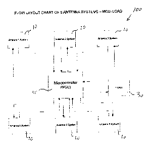
collector
device 100 of the present invention. The ambient energy collector device 100
includes
a plurality of antenna systems 10 and a micro-controller 20. The micro-
controller 20
is connected to each antenna system 10 and to a load 30. In a preferred
embodiment,
the device may include six antenna systems 10.
6
CA 02772949 2012-03-30
FIG. 2 shows a preferred embodiment of an architectural arrangement of the
circuitry
that pertains to one of the layers of the antenna system 10. Preferably, the
antenna
system 10 may have six layers. In the figures embodied herein, each block
pertains
to a circuit and the blocks are connected by arrows to show the input and
output of
each block.
The invention is preferably implemented as a multi-layer design, which may be
comprised of multiple over lapping conductor elements that act as receiving
antennas.
For example, as embodied herein these can be labeled as antenna 1, antenna 2,
antenna 3, antenna 4, antenna 5, and antenna 6. According to a preferred
embodiment of the present invention as illustrated herein, at least two
opposing
antenna arrays can be used. An exemplary embodiment is shown in FIG. 3.
According to a preferred aspect of the invention, the shape of the antenna
elements
may be geometrically designed to include, for example, flat-shaped, round-
shaped,
square-shaped, v-shaped, u-shaped layered materials. Exemplary shapes of loop
antenna elements are illustrated in FIG. 4.
In FIGS. 3 and 5, exemplary geometrical layout arrangements of the antenna
elements
are illustrated. In particular, for example, antenna 1 is a straight metal
conductor,
antenna 2 is a straight metal conductor with an inverted u-shaped bend at the
half way
point which crosses over without contact with antenna 1. As illustrated and
designated
herein, (A) is an area where antennas 1 and 2 overcross. Antenna 3 as
illustrated and
embodied herein, can be curved or u-shaped. In another preferred embodiment,
antenna 3 may be v-shaped with the bottom of the 'V' being at the point where
it
crosses over Antenna 1. As illustrated and designated herein, (B) is an area
where
antennas 3 and 1 overcross. In accordance with the invention there is no
contact
between Antenna 3 and Antenna 1. In accordance with an embodiment of the
invention, optimal performance may be obtained when the no-contact distance
between Antennas 1 and 2, and Antennas 1 and 3 is substantially the same
and/or the
area (A) is substantially equal to area (B), as defined herein. Antennas 4, 5
and 6 may
be designed similarly, as described above and illustrated herein. For optimal
performance areas A, B, C, D and F are substantially equal.
In accordance with a preferred embodiment of the invention, the antenna design
can
be expanded either by adding more layers as illustrated in FIG. 5 or by
parallel
configuration or stacking as in FIG. 5a. The Antenna frequencies may be
configured
by the use of a Programmable Tuned Antenna circuit (see FIG. 5b).
Alternatively, the
Antenna frequencies may be configured by using a Variable Capacitor with
manual
7
CA 02772949 2012-03-30
tuning, as known in the art. (see Figure 5b). The variable capacitor has a
tuning range
from about 0.47pF to about 72pF.
Primary Start-up Boost Circuit
A DC source of power or primer input may be used to start the process of
collecting
ambient energy in accordance with a preferred embodiment of the invention. For
example, the DC source of power may be, inter alia, a Solar, DC storage
device.
In one particular embodiment, an initial power capable of starting and running
the
primary circuit is from about 0.15pW to about 0.55pW. The primary circuit may
include
a DC/DC boost conversion. Typically a harvesting energy circuit includes a
voltage
doubling circuit. For example, various forms of rectifiers which can take an
AC voltage
as input and output a doubled DC voltage are used and known. However, use of
conventional harvesting of RF energy can produce only very small amounts of DC
energy.
In accordance with the invention, as embodied herein and illustrated in FIG. 6
a
primary start-up boost circuit includes a voltage boost circuit. For example,
the voltage
boost circuit of the invention can advantageously accept an input voltage of
0.01 DC
volt and yield an output voltage of 5.5 DC and a maximum output current of
1500 mA.
The output voltage can be applied to the RF Frequency Sensor Circuit.
RF Frequency Sensor Circuit.
According to an embodiment of the invention, as illustrated in FIG. 7, the RF
Frequency Sensor Circuit is capable to detect RF power signal transmitted by
wireless
transmitters. Advantageously, the RF Frequency Sensor Circuit is capable of
detecting
and measuring RF signals over a large dB dynamic range. For example, RF signal
in
a decibel scale can be precisely converted into a DC voltage. Preferably, a dB
input
dynamic range can be achieved by using cascaded RF detectors and RF limiters.
Some of the example samples of the RF signals are: 50MHz, 100MHz, 200MHz,
400MHz, 600MHz, 800MHz, 1000MHz, 1200MHz, 1400MHz, 1600MHz, 1800MHz,
2000MHz, 2200MHz, 2400MHz, 2600MHz and 3000MHz. Some example of sources
of the RF signals are: Bluetooth, Wlan, WIFI, GSM cell phone, FM Broadcast,
UHF,
VHF, and Broadband.
8
CA 02772949 2012-03-30
,
The RF Frequency Sensor Circuit can send a voltage to the antenna and can
receive
a dB response from the antenna. The dB response is known as a reference scale.
The
RF Frequency Sensor Circuit can then convert the response into a DC voltage
(see
FIG. 7). For example, the RF Frequency Sensor Circuit can receive from about
0.15pW to about 7mW of power to maintain the antenna circuit. The RF Frequency
Sensor Circuit can maintain enough power to run itself and then send the
surplus to
the Energy Collection Circuit. Preferably, RF Frequency Sensor Circuit may
recover
EMF loss from the antenna circuits where it will later be converted into
energy by the
Energy Collection Circuit.
The Energy Collection Circuit
Typically, the Energy Collection Circuit is called a Charge Pump Circuit.
Basically, the
function of the charge pump circuit can be to double the effective amplitude
of an AC
input voltage and then to convert the energy to a DC voltage on an output
capacitor,
or a rechargeable battery. A conventional energy collection circuit with
standard
capacitors is shown in FIG. 9. The conventional circuit includes fixed
capacitors, with
a fixed capacitance value.
Advantageously, according to an embodiment of the present invention, there is
provided an auto stage charge pump circuit, which preferably is not fixed to
one stage
or one capacitor value. Thus, the Energy Collection Circuit according to an
embodiment of the present invention includes a multi-stage charge pump
circuit.
Preferably, the pump circuit can obtain multiple configuration stages
resulting in a
wider range of DC output voltages. Having variable capacitors or adjustable
capacitors
or fixed array capacitors and auto multiple configuration stages can result in
a wider
range of DC output voltages (see FIGS. 9 and 17).
Referring to FIG. 16 which shows a typical simulation testing results of
charge pump
circuit stages with fixed capacitor values, it can be seen that with output
capacitance
the value of the capacitor only affects the speed of the transient response.
The bigger
the value of the output capacitance, the slower the voltage rise time. Small
Capacitance output values will raise the rise time. In accordance with an
embodiment
of the invention, it may be advantageous to include an auto adjustment over
charge
pump stages and capacitors, which can result in a wider range of DC voltage
output.
The basic function of the Energy Collection Circuit is to take a DC voltage
from the RF
Frequency Sensor Circuit and amplify it. The energy can be either stored or
sent to the
Master Controller Unit (MCU), which is described below in further detail.
9
CA 02772949 2012-03-30
Referring now to FIG. 10, included in the Energy Collection Circuit is a
Regulator
Recovery Circuit. The Regulator Recovery Circuit can act as an overflow
capacitor
circuit. Its primary function is to recover any excess capacitance energy that
is
normally lost to ground. The Regulator Recovery Circuit, by way of a
programmable
control, either outputs the energy back into the Energy Collection Circuit or
outputs the
recovered energy into the RF Frequency Sensor Circuit to assist with its
voltage
requirements.
The function of the overflow reservoir capacitor Circuit is not only to store
energy, but
also to filter out noise and ripple, and to provide decoupling between the
power supply
and the load. The capacitor can be specially constructed to allow the DC load
current
pass through the capacitor. The DC load output can go through a By-Pass
Ferrite Core
Winding. (See FIGS. 10 and 10a). According to FIG. 10 a the regulator recovery
circuit
can use both inductances and resistances.
According to an embodiment of the invention, the Energy Collection Circuit
further
includes a programmable logic control which controls the shut-off for the
Primary
Startup Boost Circuit. If the required voltage is achieved then the control
will shut off
the Primary Start-up Boost Circuit. If the value of the voltage drops below
the desired
value then the control will turn on the Primary Startup Boost Circuit.
The Master Controller Unit
Preferably, according to an embodiment of the present invention, each layer of
the
antenna includes a Primary Start-up Boost Circuit, an RF Frequency Sensor
Circuit
and an Energy Collection Circuit. The Energy Collection Circut from every
array of the
antenna can be connected to a single Master Controller Processor (MCU), as
embodied herein and illustrated in FIG. 1.
Preferably, the MCU can control all the Energy Collection Circuits. More
preferably, the
MCU can determine what energy is required to run the load and can determine
the
sum of the harvested energy collected by all of the available antennas.
According to
a preferred embodiment, the MCU can only accept what energy is needed as
determined by a programmable logic control (PLC). For example, in operation,
the
MCU can start with Antenna 1 and determine its energy value. If the amount is
satisfied the MCU can stop there and apply to the load. If the value is not
reached the
MCU can determine the energy value of Antenna 2 and so on until its desired
value
is met.
CA 02772949 2012-03-30
Variations, adaptations, and modifications to the preferred embodiments of the
invention described above are possible without departing from the scope and
essence
of the invention as described in the claims appended hereto.
11