Note : Les descriptions sont présentées dans la langue officielle dans laquelle elles ont été soumises.
CA 02772982 2012-03-02
WO 2011/026217 PCT/CA2010/001293
Title: METHOD AND APPARATUS FOR DRIVING AN
ELECTROLUMINESCENT DISPLAY
Field
[1] The described embodiments relate to electroluminescent displays.
More particularly, the described embodiments relate to methods and
apparatus for driving electroluminescent displays.
Background
[2] Illuminated displays can be a popular way of marketing or advertising.
Traditionally, such illuminated displays may employ fluorescent lighting or
other forms of light emitting bulbs or tubes as a light source.
[3] More recently, it has become possible to generate light from a flat
luminescent substrate in response to electrical stimulation of the substrate.
This effect can be used to create an electroluminescent display. However, it
is generally believed in the art that electroluminescent displays containing
large electroluminescent segments are impractical and difficult to produce due
to the unusually large amounts of power they require, with ever-reducing
luminescent output.
[4] It is desired to address or ameliorate one or more shortcomings or
disadvantages associated with existing illuminated displays and/or methods
for driving such displays, or to at least to provide a useful alternative
thereto.
Summary
[5] In one broad aspect, there is provided a method of driving an
electroluminescent segment, the electroluminescent segment comprising a
phosphor layer disposed between a first electrode and a second electrode,
the electroluminescent segment being associated with a parasitic resistance.
The method includes applying a series of first pulses to the first electrode,
the
first pulses alternating in polarity; and applying a series of second pulses
to
the second electrode for illuminating the electroluminescent segment, each of
the second pulses corresponding to a first pulse and having an opposite
-1-
CA 02772982 2012-03-02
WO 2011/026217 PCT/CA2010/001293
polarity to the corresponding first pulse, the width of each of the second
pulses being based on the parasitic resistance associated with the
electroluminescent segment.
[6] In some embodiments, the series of first pulses form a square
waveform.
[7] In other embodiments, each of the first pulses forms a ramping
waveform, and the first pulses alternate between ascending ramps and
descending ramps. In some embodiments, each of the second pulses are
aligned with a specific ramp level of the corresponding first pulse to
illuminate
the electroluminescent segment at a predetermined brightness.
[8] In some embodiments, the width of each of the first pulses is the
same as the width of the corresponding second pulse.
[9] In some embodiments, each of the second pulses discharges
and re-charges the electroluminescent segment.
[10] In some embodiments the width of each of the second pulses
controls the charge time of the electroluminescent segment, the maximum
charge time be equal to the following equation wherein y is the electric
permittivity of the electroluminescent segment, A is the area of the
electroluminescent segment, p is the electrical resistivity of the
electroluminescent segment and Rp is the parasitic resistance.
3yA
pA+Rn
[11] In some embodiments, the parasitic resistance comprises
current resistance, segment lead resistance, and cable resistance.
[12] In another broad aspect, there is provided an apparatus for
driving an electroluminescent segment, the electroluminescent segment
comprising a phosphor layer disposed between a first electrode and a second
electrode, the electroluminescent segment being associated with a parasitic
resistance. The apparatus includes a first drive circuit for applying a series
of
first pulses to the first electrode, the first pulses alternating in polarity;
and a
second drive circuit for applying a series of second pulses to the second
electrode for illuminating the electroluminescent segment, each of the second
-2-
CA 02772982 2012-03-02
WO 2011/026217 PCT/CA2010/001293
pulses corresponding to one of the first pulses and having an opposite
polarity
to the corresponding first pulse, the width of the second pulses being based
on the parasitic resistance associated with the electroluminescent segment.
[13] In some embodiments, the series of first pulses form a square
waveform.
[14] In other embodiments, the first pulses forms a ramping
waveform, and the first pulses alternate between ascending ramping
waveforms and descending ramping waveforms. In some embodiments, the
second drive circuit aligns each of the second pulses with a specific ramp
level of the corresponding first pulse in accordance with a dimming control
signal, and the apparatus further comprises a control unit for generating the
dimming control signal.
[15] In some embodiments, the width of the second pulses are varied
by the second drive circuit in accordance with a pulse width control signal;
and the apparatus further comprises a control circuit for generating the pulse
width control signal.
[16] In some embodiments, the width of each of the second pulses
controls the brightness of the illumination of the electroluminescent segment.
[17] In some embodiments, the second drive circuit provides a
current spike to the second electrode during a first portion of each second
pulse and provides a constant current to the second electrode during a
second portion of each second pulse.
[18] In some embodiments, the width of each of the first pulses is the
same as the width of the corresponding second pulse.
[19] In another broad aspect, there is provided an electroluminescent
display. The electroluminescent display includes a plurality of
electroluminescent segments, each electroluminescent segment comprising a
phosphor layer disposed between a first electrode and a second electrode,
each electroluminescent segment being associated with a parasitic
resistance; a plurality of first drive circuits, each first drive circuit
coupled to
one of the plurality of first electrodes, each first drive circuit applying a
series
of first pulses to the corresponding first electrode, the first pulses
alternating in
-3-
CA 02772982 2012-03-02
WO 2011/026217 PCT/CA2010/001293
polarity; and a plurality of second drive circuits, each second drive circuit
coupled to one of the plurality of second electrodes, each second drive
circuit
applying a series of second pulses to the corresponding second electrode for
illuminating the corresponding electroluminescent segment, each of the
second pulses corresponding to one of the first pulses and having an opposite
polarity to the corresponding first pulse, the width of the second pulses
being
based on the parasitic resistance associated with the corresponding
electroluminescent segment.
[20] In some embodiments, the electroluminescent display also
includes a control unit for generating a plurality of pulse width control
signals,
wherein each of the second drive circuits varies the width of the
corresponding second pulses in accordance with one of the pulse width
control signals.
[21] In some embodiments, the width of each series of second
pulses controls the brightness of the illumination of the corresponding
electroluminescent segment.
[22] In another broad aspect, there is provided an electroluminescent
display. The electroluminescent display includes: a common electrode; a
plurality of electroluminescent segments mounted on the common electrode,
each segment comprising a segment electrode and a phosphor layer
disposed between the common electrode and the segment electrode, each
electroluminescent segment being associated with a parasitic resistance; a
first drive circuit coupled to the common electrode, the first drive circuit
applying a series of first pulses to the common electrode, the first pulses
alternating in polarity; and a plurality of second drive circuits, each second
drive circuit coupled to one of the plurality of second electrodes, each
second
drive circuit applying a series of second pulses to the corresponding second
electrode for illuminating the corresponding electroluminescent segment, each
of the second pulses corresponding to one of the first pulses and having an
opposite polarity to the corresponding first pulse, the width of the second
pulses being based on the parasitic resistance associated with the
corresponding electroluminescent segment.
- 4 -
CA 02772982 2012-03-02
WO 2011/026217 PCT/CA2010/001293
[23] In another broad aspect, there is provided a method of driving
an electroluminescent segment, the electroluminescent segment comprising a
phosphor layer disposed between first and second electrodes. The method
includes measuring intrinsic properties of the electroluminescent segment;
measuring parasitic resistance associated with the electroluminescent
segment; calculating a charge time for the electroluminescent segment based
on the intrinsic properties and the parasitic resistance; storing the
calculated
charge time in memory; applying a series of first pulses to the first
electrode,
the first pulses alternating in polarity; and applying a series of second
pulses
to the second electrode for illuminating the electroluminescent segment, each
second pulse corresponding to one of the first pulses and having an opposite
polarity to the corresponding first pulse, the width of the second pulses
being
based on the stored charge time.
Brief Description of the Drawings
[24] A preferred embodiment of the present invention will now be described
in detail with reference to the drawings, in which:
FIG. 1 is a side view of an electroluminescent segment in accordance
with an embodiment;
FIG. 2 is a circuit diagram of an impedance network that models the
electroluminescent segment of FIG. 1;
FIG. 3 is a block diagram of an apparatus for driving an
electroluminescent display in accordance with an embodiment;
FIG. 4 is a schematic of the voltage waveforms generated by a
dimming common plane driver and a segment driver in accordance with an
embodiment;
FIG. 5 is a schematic of the voltage waveforms generated by a non-
dimming common plane driver and a segment driver in accordance with an
embodiment;
FIG. 6 is a circuit diagram of a dimming common plane driver in
accordance with an embodiment;
-5-
CA 02772982 2012-03-02
WO 2011/026217 PCT/CA2010/001293
FIG. 7 is a circuit diagram of a non-dimming common plane driver in
accordance with an embodiment;
FIG. 8 is a circuit diagram of the segment driver of FIG. 3 in
accordance with an embodiment;
FIG. 9 is a schematic of the current waveform of the segment driver of
FIG. 8 in accordance with an embodiment;
FIG. 10 is a block diagram of an apparatus for driving an
electroluminescent display in accordance with an alternate embodiment; and
FIG. 11 is a schematic of the voltage waveform generated by a pair of
segment drivers of FIG. 10 in accordance with an embodiment.
Description of Exemplary Embodiments
[25] Some of the embodiments described herein relate to methods and
apparatus for driving an electroluminescent display in a manner in which the
power required is reduced. In some embodiments, the brightness of the
display may be varied in a controlled manner.
[26] An electroluminescent display emits light in response to the application
of a high-frequency voltage. An electroluminescent display may be divided
into a number of electroluminescent segments that can be individually
illuminated. Optionally, the electroluminescent segments may be arranged to
form a matrix or grid. In other embodiments, the electroluminescent
segments may have other shapes and arrangements.
[27] Each electroluminescent segment typically comprises an
electroluminescent substance (i.e. a phosphor substance) disposed between
two electrodes. In some cases, one of the electrodes is common to some or
all electroluminescent segments in a display. In other cases, the electrodes
of
each electroluminescent segment are electrically isolated from those of other
segments. Application of a sufficiently high frequency alternating current
(AC)
voltage across the electrodes of an electroluminescent segment will produce
electroluminescence or illumination of the segment.
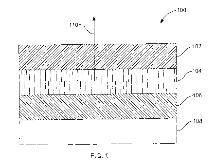
[28] Reference is now made to FIG. 1, in which an exemplary
electroluminescent segment 100 is illustrated. The electroluminescent
-6-
CA 02772982 2012-03-02
WO 2011/026217 PCT/CA2010/001293
segment 100 comprises a number of parallel layers 102, 104, 106, and 108.
In the embodiment shown in FIG. 1, the electroluminescent segment 100 is
comprised of four layers, a front electrode layer 102, an electroluminescent
layer 104, a dielectric layer 106 and a rear electrode layer 108. When a
voltage is applied across the front and rear electrode layers 102 and 108, the
electroluminescent layer 104 is activated and emits light in the direction
indicated by arrow 110.
[29] The front electrode layer 102 is comprised of an optically transparent
and electrically conductive material such as indium-tin-oxide (ITO).
[30] The electroluminescent layer 104 is formed on the front electrode layer
102. The electroluminescent layer 104 may be made of any suitable phosphor
such as copper activated zinc sulfide (ZnS), or manganese (Mn) activated
zinc sulfide (ZnS). In some cases, the electroluminescent layer 104 is 20-
micron thick zinc sulfide (ZnS) doped with a small amount of copper (CU2+)
ions.
[31] After the electroluminescent layer 104 is the dielectric layer 106. The
dielectric layer 106 may be comprised of electrically insulating material that
provides a barrier to the flow of electronics. Suitable insulating material
includes conventional dielectric powder, such as white dielectric powder, in a
suitable binder. In one embodiment, the dielectric layer 106 is 33-micron
thick
barium titanate (BaTiO3).
[32] The rear electrode layer 108 is formed on the dielectric layer 106 and
may be comprised of any suitable electrically conductive material. The rear
electrode layer 108 may be comprised of the same material as the front
electrode layer 102, such as ITO, or different material. For example, the rear
electrode layer 108 may be comprised of a suitable opaque material such as
a silver (Ag), gold (Au) or graphite-based material. In some cases, the rear
electrode 108 is silver (Ag).
[33] In some cases, the electroluminescent segment 100 may comprise
additional layers. For example, the electroluminescent segment 100 may
further comprise an encapsulation layer that acts as a water barrier to
protect
the electroluminescent layer 104 from atmospheric moisture. The
- 7 -
CA 02772982 2012-03-02
WO 2011/026217 PCT/CA2010/001293
electroluminescent segment 100 may also include a substrate upon which the
layers are formed. The substrate may be comprised of any suitable
transparent or translucent material, such as glass or plastic. The substrate
may be rigid or flexible.
[34] The electroluminescent segment 100 acts as a photoemissive
capacitor. Specifically, the electroluminescent segment 100 is charged to a
predetermined voltage (e.g. 160 V) which generates an electric field (e.g. 2.5
x 106 Vm"2). The externally applied electric field is then suddenly reversed,
thereby discharging the electroluminescent segment 100 and recharging it
with the opposite polarity. During the repolarization, the electrons in the
semiconductive electroluminescent layer 104 (e.g. the zinc sulfide (ZnS)
layer) collide with the dopant ions (e.g. the copper (CU2+) ions) with
sufficient
energy to ionize then. The ionized impurity extracts an electron from the
conduction band of the electroluminescent layer 104 (e.g. the zinc sulfide
(ZnS) layer) putting it in a metastable electronically excited state, which
subsequently relaxes to the ground state photoemmissively. Accordingly,
current is passed and light is emitted only during the repolarization periods,
which typically only last a few microseconds.
[35] Reference is now made to FIG. 2, which illustrates an impedance
network 200 that can be used to model the electroluminescent segment 100.
The impedance network 200 comprises a capacitor 202, a first resistor 204
and a second resistor 206. The capacitor 202 represents the capacitance of
the electroluminescent segment 100, the first resistor 204 represents the
resistance of the electroluminescent segment 100, and the second resistor
206 represents the resistance of the DC leakage paths through the capacitor
202. The capacitance C202 of the capacitor 202 and the resistances R204 and
R206 of the first and second resistors 204 and 206 respectively, can be
represented by the intrinsic properties of the electroluminescent segment 100
as is shown in equation (1) where A is the area of the electroluminescent
segment, y is the electric permittivity of the electroluminescent segment, and
p
is the electrical resistivity of the electroluminescent segment.
-8-
CA 02772982 2012-03-02
WO 2011/026217 PCT/CA2010/001293
C302 = YA
R304 P (1)
A
R306 306
A
[36] Typically the second resistor 206 is insignificant and thus can be
ignored. If the second resistor 206 is ignored, the relaxation time T of the
circuit can be represented by equation (2). It can be seen from equation (2)
that the relaxation time z is dependent only on the intrinsic properties of
the
electroluminescent segment, and not on extrinsic factors such as the size
(area) or geometry of the electroluminescent segment.
T = R204C202 = A (yA) = py (2)
[37] The electroluminescent segment 100 may be illuminated by a driving
circuit or apparatus that supplies a series of alternating positive and
negative
pulses to the electrodes of the electroluminescent segment 100. Each pulse
causes a discharge and subsequent recharge of the capacitor 202. As
described above, it is the discharge that triggers illumination of the
electroluminescent segment 100. One cycle comprises both a positive and
negative pulse and each half cycle comprises a single negative or positive
pulse. The rate at which a cycle repeats is referred to as the frequency f:
[38] The electroluminescent segment 100 presents a complex impedance
to the driving circuit, and like any complex impedance, energy is consumed
only by the real component. In addition, the energy required to charge the
capacitor 202 does not contribute to the power dissipation, and is returned
during the subsequent half cycle. Accordingly, the power dissipation P(t) of
an electroluminescent segment 100 is given by equation (3), and the energy
E1 consumed by the electroluminescent segment during each half cycle is
given by equation (4) where i(t) is the current flowing across the
electroluminescent segment 100. The current i(t) can be represented by
equation (5) where V0 is the maximum voltage of the driving pulses.
P(t) = i2(t)R204 (3)
- 9 -
CA 02772982 2012-03-02
WO 2011/026217 PCT/CA2010/001293
Ec = R204 f i2dt (4)
i(t) = Vo eRz04c1,2 (5)
R204
[39] The integration is taken over the entire half cycle, which is typically
much longer than the relaxation time T of equation (2). Accordingly, the
integral is taken from zero to infinity so that the energy consumed by the
electroluminescent segment 100 during each half cycle is reduced to equation
(6). Since there are two pulses per cycle, the total power dissipation per
cycle
is represented by equation (7).
2
EC = C202V0 (6)
2
P = 2JEc = .JC202Vo (7)
[40] An examination of equation (7) reveals that the total power dissipation
P is independent of the resistance in the circuit, even though the resistance
is
the dissipative element. The total resistance in the circuit typically
includes
not only the intrinsic resistance R204 of the electroluminescent segment 100
itself, but also the parasitic resistance R. in the circuit. The parasitic
resistance R. is defined as the sum of the resistances introduced in the
cables, backplane and screen printed electrodes. Accordingly, the efficiency
of the electroluminescent segment 100 can be improved by decreasing the
parasitic resistance RP without increasing the power consumption.
[41] The power coefficient c is defined as the percentage of the power
delivered to the electroluminescent segment 100 (i.e. the intrinsic resistance
R204) as opposed to the parasitic resistance RP and is represented by equation
(8). Equation (8) can be re-written in terms of the intrinsic properties of
the
electroluminescent segment 100 as shown in equation (9).
= R204 (8)
RP + R204
P (9)
p + ARP
-10-
CA 02772982 2012-03-02
WO 2011/026217 PCT/CA2010/001293
[42] An examination of equation (9) reveals that when the parasitic
resistance RP is zero, the power coefficients is equal to 1 and maximum
power is delivered to the electroluminescent segment 100. Where, however,
the parasitic resistance RP is greater than zero, the power coefficient s and
thus the efficiency of the electroluminescent segment 100 decreases with the
increasing electroluminescent segment area A. Accordingly, if the parasitic
resistance RP is greater than zero, a larger (i.e. greater area)
electroluminescent segment 100 will require more power to achieve the same
level of luminescence. However, it will be illustrated below that the affect
of
the size (i.e. area) of the electroluminescent segment 100 on the power
requirements can be significantly reduced by carefully choosing the driving
pulse profiles.
[43] The power coefficient s may be re-written in terms of the
electroluminescent segment 100 capacitance C202 instead of the
electroluminescent segment area A as shown in equation (10).
E YP (10)
(yp+C202RP)
[44] When the power coefficients is equal to 1, the luminescent intensity I is
directly proportional to the consumed power P as shown in equation (11),
where x is defined as the luminescent efficiency coefficient. Where, however,
the power coefficient s is greater than 1, the luminescent intensity I is
reduced
in accordance with the power coefficients as shown in equation (12).
IKP (11)
I = KKEP (12)
[45] Equation (12) can be rearranged so that the luminescent efficiency
coefficient is represented by equation (13).
(13)
~c= I(yp+C,02RP)
.fpVe2 yC,02
[46] The luminescent output per unit of area I/A is given by equation (14).
Equation (14) can then be rearranged as shown in equation (15) to give the
luminescent intensity I.
-11-
CA 02772982 2012-03-02
WO 2011/026217 PCT/CA2010/001293
~ yKE (14)
A = JV2
I=fV0yKA (15)
[47] Accordingly, the luminescent characteristics of an electroluminescent
segment 100, such as the luminescent efficiency coefficient x and the power
efficiency E, can be calculated from equations (13) and (10) respectively by
measuring RP and C202. Then the luminescent intensity I can be calculated
from equation (15). The total power demand on the power supply can then be
calculated from equation (16).
P = fV02yA (16)
[48] Once RP and C202 have been measured, the time required to charge the
capacitor 202 can be calculated. Specifically, the time t, to charge the
capacitor 202 to x% of the maximum voltage is expressed in equation (17). If
it is assumed that the capacitor 202 is charged when it has reached 95% of its
maximum voltage, equation (17) reduces to equation (18).
tc = -(R201 + Rp)C202 In(I - x /100) (17)
t, = -(R204 + Rp)C2021n(0.05) = 3(R204 + Rp)C202 = pA yA
RP (18)
[49] Reference is now made to FIG. 3, in which an apparatus 300 for driving
an electroluminescent display 302 in accordance with an embodiment is
illustrated. The apparatus 300 is designed to take advantage of the
observations made by the inventors as described above. Particularly, the
apparatus 300 is designed to take advantage of the relationship between the
charge time t, and parasitic resistance RP to reduce the power consumption of
the electroluminescent display 302.
[50] The electroluminescent display 302 includes one or more
electroluminescent segments 100a and 100b that are individually coupled to
the apparatus 300. As described above, each electroluminescent segment
100a and 100b comprises an electroluminescent substance (i.e. phosphor
substance) disposed between two electrodes. At least two of the
electroluminescent segments 100a and 100b have a common electrode. In
the embodiment shown in FIG. 3, all of the electroluminescent segments 100a
-12-
CA 02772982 2012-03-02
WO 2011/026217 PCT/CA2010/001293
and 100b share a common electrode. However, in other embodiments, there
may be more than one common electrode where each common electrode is
shared by two or more electroluminescent segments. In some embodiments,
the electroluminescent segments 100a and 100b are arranged to form a
matrix or grid. In other embodiments, the electroluminescent segments 100a
and 100b may have other shapes and arrangements.
[51] The apparatus 300 comprises a common plane driver 304, one or more
segment drivers 308a and 308b (typically one for each electroluminescent
segment 100a and 100b), a power module 310 and a control unit 312. The
common plane driver 304 and the segment drivers 308a and 308b work
together to provide an AC voltage across one or more electroluminescent
segments 100a and 100b to illuminate the one or more electroluminescent
segments 100a and 100b. The common plane driver 304 may be a non-
dimming common plane driver or a dimming common plane driver. A non-
dimming common plane driver allows the electroluminescent segments to be
either illuminated or not, whereas a dimming common plane driver allows the
luminescence or brightness of the electroluminescent segments to be varied
in a controlled manner.
[52] For example, a non-dimming common plane driver may supply a series
of pulses to the common electrode (i.e. the front electrode) of the one or
more
electroluminescent segments 100a and 100b. Each segment driver 308a and
308b then supplies a series of pulses of opposite polarity to the non-dimming
common electrode pulses to the other electrode of one of the
electroluminescent segments 100a or 100b. The width of the segment driver
308a or 308b pulses is typically smaller than the width of the non-dimming
common plane driver pulses. Each segment driver pulse generates a voltage
potential across the corresponding electroluminescent segment 100a or 100b,
which causes a discharge and subsequent recharge of the electroluminescent
segment 100a or 100b. Light is emitted during the discharge. An exemplary
set of voltage waveforms generated by a non-dimming common plane driver
and a segment driver 308a or 308b is illustrated in FIG. 4. An exemplary non-
dimming common plane driver will be described in reference to FIG. 7.
-13-
CA 02772982 2012-03-02
WO 2011/026217 PCT/CA2010/001293
[53] A dimming common plane driver, on the other hand, may supply a
series of upward (ascending) and downward (descending) voltage ramps to
the common electrode (i.e. the front electrode) of the one or more
electroluminescent segments 100a and 100b. Each segment driver 308a and
308b then supplies a series of pulses of opposite polarity to the direction of
the ramp to the other electrode of one of the electroluminescent segments
100a or 100b. For example, if the dimming common plane driver ramp is an
upward (or ascending) ramp, then the corresponding segment driver pulse will
be negative, and if the ramp is a downward (or descending) ramp, then the
corresponding segment driver pulse will be positive. The width of the
segment driver 308a or 308b pulses is typically smaller than the width of the
dimming common plane driver ramps. Each segment driver pulse generates
a voltage potential across the corresponding electroluminescent segment
100a or 100b, which causes a quick discharge and a subsequent recharge of
the electroluminescent segment 100a or 100b. The quick discharge results in
illumination of the corresponding electroluminescent segment. The amount of
illumination or brightness will depend on the voltage produced by the dimming
common plane driver at the time the corresponding segment driver pulse is
triggered. Specifically, the greater the difference between the segment driver
pulse voltage and the dimming common plane driver ramp voltage, the
greater the brightness. An exemplary set of voltage waveforms generated by
a dimming common plane driver and a segment driver 308a or 308b is
illustrated in FIG. 5. An exemplary dimming common plane driver will be
described in reference to FIG. 6.
[54] The power module 310 is electrically coupled or connected to the
common plane and segment drivers 304, 308a and 308b to provide power to
the drivers 308a and 308b. In one embodiment, the power module 310
generates and provides three DC voltages 314, 316 and 318 to the drivers.
The first DC voltage 314 will be referred to as the positive voltage rail and
controls the maximum voltage of the common plane and segment driver
pulses and ramps. The second DC voltage 316 will be referred to as the
negative voltage rail and controls the minimum voltage of the common plane
-14-
CA 02772982 2012-03-02
WO 2011/026217 PCT/CA2010/001293
and segment driver pulses and ramps. The third DC voltage 318 will be
referred to as the digital voltage signal and provides power to various
electrical components within the common plane and segment drivers. In other
embodiments, the power module 310 may provide other voltages.
[55] The control unit 312 is electrically coupled or connected to the segment
drivers 308a and 308b to provide timing information to the segment drivers
308a and 308b. The control unit 312 may, for example, comprise a memory or
other similar storage device that stores a sequence of commands to control
the illumination of the electroluminescent segments 100a and 100b. The
sequence of commands may include which of the electroluminescent
segments to illuminate when, for how long, and at what brightness.
[56] In one embodiment, the control unit 312 generates high and low control
signals for each segment driver 308a and 308b which control the timing or
width, or both, of the pulses generated by the segment drivers 308a and
308b. Where the high and low control signals are used to control the timing of
the pulses generated by the segment drivers 308a and 308b to align them
with a certain ramp level of the ramping waveform generated by a dimming
common plane driver, the high and low control signals may be referred to as
dimming control signals. Where the high and low control signals are used to
control the width of the pulses generated by the segment drivers 308a and
308b the high and low control signals may be referred to as pulse width
control signals.
[57] Reference is now made to FIG. 4, which illustrates the voltage
waveforms 402 and 404 generated by a non-dimming common plane driver
and a segment driver 308a or 308b, respectively in accordance with an
embodiment. As can be seen from FIG. 4, a non-dimming common plane
driver may supply a square wave to the common electrode (i.e. the front
electrode), and the segment driver 308a or 308b may supply a series of
complementary pulses of opposite polarity to the other electrode (i.e. the
rear
or back electrode 108) of one electroluminescent segment 100a or 100b. As
described above, each segment driver pulse generates a voltage potential
across the corresponding electroluminescent segment 100a or 100b, which
-15-
CA 02772982 2012-03-02
WO 2011/026217 PCT/CA2010/001293
causes a discharge and then subsequent recharge of the electroluminescent
segment 100a or 100b. Light is emitted by the corresponding
electroluminescent segment 100a or 100b during the discharge.
[58] As described in equation (18), the charge time of an electroluminescent
segment 100a or 100b is based on the parasitic resistance RP of the
electroluminescent segment circuit. Since the width of the pulse determines
the period of time voltage is supplied across the electroluminescent segment
(and thus the time the electroluminescent segment is charged), the pulse
width of the segment driver pulse is also dependent on the parasitic
resistance RP. Where the parasitic resistance RP is equal to zero, equation
(18) reduces to 3y/p. Therefore the absolute minimum pulse width to achieve
the maximum luminescence is 3y/p. Where, for example, y is equal to 490
pF/cm2 and p is equal 930 Q/cm2 the minimum width of the segment pulse to
achieve the maximum luminescence is roughly 1.5 s. Introducing parasitic
resistance R. into the circuitry increases the charge time (and thus the pulse
width) to achieve the maximum luminescence at a rate of 37R,, per unit area.
Accordingly, if the parasitic resistance RP of the electroluminescent segment
100a or 100b is known, the charge time (and thus pulse width) to achieve the
maximum luminescence can be determined from equation (18). If the pulse
width (and thus charge time) is less than the pulse width calculated according
to equation (18), the electroluminescent segment 100a or 100b will not
achieve maximum luminescence. On the other hand, if the pulse width (and
thus charge time) is greater than the pulse width calculated according to
equation (18), power will be wasted.
[59] Typically, each segment driver 308a or 308b that shares a particular
common electrode triggers its pulses at different times during the cycle. For
example, the pulses from the first segment driver 308a would typically not
overlap in time with the pulses generated by the second segment driver 308b.
Accordingly, the frequency of the square wave generated by the non-dimming
common plane driver is typically selected to be long enough to allow each of
-16-
CA 02772982 2012-03-02
WO 2011/026217 PCT/CA2010/001293
the electroluminescent segments sharing a common electrode to be activated
by a segment pulse during one half cycle.
[60] Reference is now made to FIG. 5, which illustrates the waveforms 502
and 504 generated by a dimming common plane driver and a segment driver
308a or 308b, respectively. As can be seen from FIG. 5, a dimming common
plane driver supplies a ramping waveform to the common electrode (i.e. the
front electrode), and, similar to FIG. 4, the segment driver 308a or 308b
supplies a series of opposite polarity pulses to the other electrode (i.e. the
rear electrode) of one electroluminescent segment 100a or 100b. The
segment driver pulses of FIG. 5 operate in the same manner as the segment
driver pulses shown in FIG. 4. Specifically, each segment driver pulse
generates a voltage potential across the corresponding electroluminescent
segment, which causes a discharge and subsequent recharge of the
electroluminescent segment 100a or 100b. Light is emitted by the
corresponding electroluminescent segment 100a or 100b during the
discharge. However, now the segment driver pulses can be fired at specific
points along the ramp affording a continuum of light intensity.
[61] Specifically, the brightness is determined by the difference between the
segment driver pulse voltage and the dimming common plane driver ramp
voltage. The greater the difference between the two voltages, the greater the
brightness. Conversely the smaller the difference between the two voltages,
the dimmer the illumination. Accordingly, the segment driver pulses can be
triggered at different points along the ramp to either increase or decrease
the
difference between the voltages (and thus the brightness). The flat portions
of
the common plane waveform typically provide the greatest difference between
the common plane driver ramp voltage and the segment driver pulse voltage
and thus can be used to achieve maximum light intensity.
[62] In one embodiment, such as the embodiment shown in FIG. 5, the
segment drivers are configured to generate pulses that are opposite in
polarity
to the direction of the ramp. For example, when the common driver ramp is
an upward or ascending ramp, the segment drivers generate negative pulses,
-17-
CA 02772982 2012-03-02
WO 2011/026217 PCT/CA2010/001293
and when the common driver ramp is a downward or descending ramp, the
segment drivers are configured to generate positive pulses.
[63] Therefore for an ascending ramp, the higher the voltage of the dimming
common plane driver waveform at the time the segment driver pulse is
triggered, the brighter the illumination. For example, if the segment driver
pulse is triggered in the earlier part of the upward ramp (i.e. when the ramp
voltage is lower), the intensity or brightness of the illumination of the
corresponding electroluminescent segment will be lower. Conversely, if the
segment driver pulse is triggered in the latter part of the upward ramp (i.e.
when the ramp voltage is higher), the intensity or brightness of the
illumination
of the corresponding electroluminescent segment 100a or 100b will be higher.
The converse is true for a descending ramp, the lower the voltage of the
dimming common plane driver waveform at the time the segment driver pulse
is triggered, the more dim the illumination.
[64] Reference is now made to FIG. 6, in which a dimming common plane
driver 600 in accordance with an exemplary embodiment is illustrated. The
dimming common plane driver 600 receives three DC voltage signals (the
positive voltage rail 314, the negative voltage rail 316 and a digital voltage
signal 318) from the power module 310 and generates the ramping waveform
502 shown in FIG. 5. In the embodiment shown in FIG. 6, the dimming
common plane driver 600 comprises four capacitors 602, 604, 606 and 608;
seven diodes 610, 612, 614, 616, 618, 620 and 622; eleven transistors 624,
626, 628, 630, 632, 634, 636, 638, 640, 642 and 644; thirteen resistors 646,
648, 650, 652, 654, 656, 658, 660, 662, 664, 666, 668 and 670; and a
sequencer 672.
[65] The sequencer 672 controls the operation of the dimming common
plane driver 600. More specifically, the sequencer 672 controls the timing
(i.e.
frequency) of the waveform generated by the dimming common plane driver
600. In one embodiment, the sequencer 672 is pre-loaded with the timing
information. In other embodiments, the timing information is received
dynamically from the control unit 312. The sequencer 672 may be
implemented by a microcontroller, such as the PIC16F876 microcontroller.
-18-
CA 02772982 2012-03-02
WO 2011/026217 PCT/CA2010/001293
[66] At the beginning of each frequency cycle the sequencer 672 sets the
bases of the fourth and fifth transistors 630 and 632 high. This drives the
second and fourth transistors 626 and 628 into conduction, causing the third
capacitor 606 to charge to the positive voltage rail 314 through the third
resistor 650.
[67] This generates the upward (or ascending) ramping portion of the
waveform 502 shown in FIG. 5. The time constant z of the RC circuit is equal
to R550 * C6o6 where R650 is the resistance in ohms of the third resistor 650
and
C606 is the capacitance in Farads of the third capacitor 606. The time which
is required to charge the capacitor to x % of its maximum voltage is expressed
in equation (19).
T=zln(1-x/100) (19)
[68] In some embodiments, the capacitor is deemed to be charged when it
reaches 95% of its maximum voltage. This reduces equation (19) to 3z. Thus
the capacitor will be charged within 3 time constants. Firing the segment
driver pulse anytime within this charging period will illuminate the
corresponding electroluminescent segment 100a or 100b with varying
intensities.
[69] Typically, the segment drivers are configured to generate pulses that
are opposite in polarity to the direction of the ramp generated by the dimming
common plane driver. For example, the segment drivers may generate a
negative pulse when the ramp is an upward or ascending ramp, and a positive
pulse when the ramp is a downward or descending ramp. Accordingly, during
the first frequency half cycle the higher the voltage of the dimming common
plane driver waveform at the time the segment driver pulse is triggered, the
brighter the illumination. For example, if the segment driver pulse is
triggered
in the earlier part of the upward ramp (i.e. when the ramp voltage is lower),
the intensity or brightness of the illumination of the corresponding
electroluminescent segment will be lower. Conversely, if the segment driver
pulse is triggered in the latter part of the upward ramp (i.e. when the ramp
voltage is higher), the intensity or brightness of the illumination of the
corresponding electroluminescent segment 100a or 100b will be higher.
-19-
CA 02772982 2012-03-02
WO 2011/026217 PCT/CA2010/001293
[70] Once the third capacitor 606 has been charged to the positive voltage
rail 314, the voltage is held constant. This will be referred to as the "flat
period" of the first frequency half cycle. The maximum luminescence or
brightness is achieved when the segment driver pulse is triggered during the
"flat period."
[71] At the end of the first frequency half cycle, the sequencer 672 drives
the bases of the fourth and fifth transistors 630 and 632 low. This drives the
ninth transistor 640 into conduction, causing the third capacitor 606 to
charge
to the negative voltage rail 316 through the seventh resistor 658. This
generates the downward (or descending) ramping portion of the waveform
shown in FIG. 5. The time constant T of the RC circuit is equal to R658 * C606
where R658 is the resistance in ohms of the seventh resistor 658 and C606 is
the capacitance in Farads of the third capacitor 606. The time which is
required to charge the capacitor to x % of its maximum charge is expressed in
equation (19).
[72] In some embodiments, the capacitor is deemed to be charged when it
reaches 95% of its maximum charge. This reduces equation (19) to 3T. Thus
the capacitor will be charged within 3 time constants. Firing the segment
driver pulse anytime within this charging period will illuminate the
corresponding electroluminescent segment 100a or 100b with varying
intensities.
[73] As described above, the segment drivers may be configured to
generate pulses that are opposite in polarity to the direction of the ramp.
For
example, the segment drivers may generate a negative pulse when the ramp
is an upward or ascending ramp, and a positive pulse when the ramp is a
downward or descending ramp. Accordingly, in the second half cycle, the
lower the voltage of the dimming common plane driver at the time the
segment driver pulse is triggered, the brighter the illumination. For example,
if
the segment driver pulse is triggered in the earlier part of the downward ramp
(i.e. when the ramp voltage is higher), the intensity or brightness of the
illumination of the corresponding electroluminescent segment will be lower.
Conversely, if the segment driver pulse is triggered in the latter part of the
-20-
CA 02772982 2012-03-02
WO 2011/026217 PCT/CA2010/001293
downward ramp (i.e. when the ramp voltage is lower), the intensity or
brightness of the illumination of the corresponding electroluminescent
segment will be higher.
[74] Once the third capacitor 606 has been charged to the negative voltage
rail 316, the voltage is held constant. This will be referred to as the "flat
period" of the second frequency half cycle. The maximum luminescence or
brightness may be achieved when the segment driver pulse is triggered
during the "flat period."
[75] The complete ramping waveform 502 shown in FIG. 5 appears on the
gate of the sixth transistor 634. The sixth transistor 634 is configured as a
source follower and drives a voltage follower output stage comprising the
first
and third transistors 624 and 628 on the high side, and the tenth and eleventh
transistors 642 and 644 on the low side.
[76] The seventh and eighth transistors 636 and 638 and the sixth and
eighth resistors 656 and 660 act as current limiters. Specifically, the
seventh
and eighth transistors 636 and 638 and the sixth and eighth resistors 656 and
660 limit the current flowing through the voltage follower output stage (e.g.
first and third transistors 624 and 628 or tenth and eleventh transistors 642
and 644).
[77] The third and seventh diodes 614 and 622 work in conjunction with the
first and fourth capacitors 602 and 608 to shunt transient overvoltages causes
by the voltage doubling effect of the corresponding electroluminescent
segment 100a or 100b capacitive load during switching.
[78] The first and second diodes 610 and 612 eliminate base leakage
currents assuring definite cut-off of the fifth transistor 632.
[79] The sequencer 672 may also generate one or more synchronization
signals at a predetermined time before the start of each half cycle so that
the
segment drivers 308a and 308b can synchronize their pulses with the
waveform generated by the dimming common plane driver 600. In some
embodiments, the sequencer 672 generates two synchronization signals. The
first synchronization signal is generated at a predetermined time prior to the
start of the first half cycle, and the second synchronization signal is
generated
-21 -
CA 02772982 2012-03-02
WO 2011/026217 PCT/CA2010/001293
at a predetermined time prior to the start of the second half cycle. In other
embodiments, the sequencer 672 may generate only a single synchronization
signal which is used to carry the timing information for both half cycles. In
some embodiments, the predetermined time is 10 s. However, other
suitable predetermined times may be used.
[80] In one embodiment, the components of the dimming common plane
driver 600 have the values and types as set out in Table 1.
Table 1
Element Type Value/Part
Number
602 Capacitor 0.1 F 100 V
604 Capacitor 0.1 F
606 Capacitor 560 pF
608 Capacitor 0.1 F 100 V
610 3 Amp Medium Power 1 N4148
Silicon Rectifier Diode
612 3 Amp Medium Power 1 N4148
Silicon Rectifier Diode
614 3 Amp Medium Power RF071
Silicon Rectifier Diode
616 3 Amp Medium Power RF071
Silicon Rectifier Diode
618 3 Amp Medium Power RF071
Silicon Rectifier Diode
620 3 Amp Medium Power RF071
Silicon Rectifier Diode
622 3 Amp Medium Power RF071
Silicon Rectifier Diode
624 NPN Bipolar Transistor MMST5551
626 PNP Bipolar Transistor MMST5401
-22-
CA 02772982 2012-03-02
WO 2011/026217 PCT/CA2010/001293
628 NPN Darlington Bipolar 2SD1 535
Transistor
630 NPN Bipolar Transistor MMST5551
632 PNP Bipolar Transistor MMST5401
634 N-Channel MOSFET ZVN4424
636 NPN Bipolar Transistor MMST5551
638 PNP Bipolar Transistor MMST5401
640 NPN Bipolar Transistor MMST5551
642 PNP Darlington Bipolar FJPF9020
Transistor
644 PNP Bipolar Transistor MMST5401
646 Resistor 75 KQ
648 Resistor 4.7 KQ
650 Resistor 150 KQ
652 Resistor 2.4 KQ
654 Resistor 4.7 KQ
656 Resistor 1R
658 Resistor 150 KQ
660 Resistor 1R
662 Resistor 75 KQ
664 Resistor 75 MQ
666 Resistor 2.2 MQ
668 Resistor 75 KQ
670 Resistor 2.4 KQ
670 Sequencer PIC12F629-I/SN
[81] Reference is now made to FIG. 7, in which a non-dimming common
plane driver 700 in accordance with an embodiment is illustrated. The non-
dimming common plane driver 700 receives three DC voltage signals (the
positive voltage rail 314, the negative voltage rail 316 and a digital voltage
signal 318) from the power module 310 and generates the square waveform
-23-
CA 02772982 2012-03-02
WO 2011/026217 PCT/CA2010/001293
402 shown in FIG. 4. In the embodiment shown in FIG. 7, the non-dimming
common plane driver 700 comprises three capacitors 702, 704 and 706; four
diodes 708, 710, 712, and 714; four transistors 716, 718, 720 and 722; nine
resistors 724, 726, 728, 730, 732, 734, 736, 738, and 740 and a sequencer
742.
[82] The sequencer 742 controls the operation of the non-dimming common
plane driver 700. More specifically, the sequencer 742 controls the timing
(i.e.
frequency) of the voltage waveform generated by the non-dimming common
plane driver 700. In one embodiment, the sequencer 742 is pre-loaded with
the timing information. In other embodiments, the sequencer 742 may receive
the timing information dynamically from the control unit 312. The sequencer
742 may be implemented by a microcontroller, such as the PIC16F876
microcontroller.
[83] At the beginning of each frequency cycle the sequencer 742 sets the
base of the second transistor 718 high. The third and fourth resistors 728 and
730 form a resistive divider that raises the gate of the first transistor 716
to a
percentage of the positive voltage rail 314. Specifically, the resistive
divider
raises the gate of the first transistor 716 to R730/(R728 + R73o)* Positive
Voltage
Rail 314 where R728 is the resistance of the third resistor 728 and R730 is
the
resistance of the fourth resistor 730. For example, where the third and fourth
resistors 728 and 730 have resistances of 3.9 KQ and 18 KQ respectively and
the positive voltage rail 314 is 80 V, the gate of first transistor 716 will
be
roughly 65 V, or 15 V below the positive voltage rail 314.
[84] This drives the first transistor 716 into saturation with a light load.
However, under heavy load conditions, the first transistor 716 acts as a
source follower, preventing the voltage drop across the first resistor 724
from
exceeding a predetermined voltage (i.e. 13V). Therefore, current through the
first transistor's 716 drain is limited to the predetermined voltage/R724
where
R724 is the resistance of the first resistor 724. For example, where the
predetermined voltage is 13 V and the resistance R724 of the first resistor
724
is 82 Q the current through the first transistor's 716 drain is limited to 13
V/82
-24-
CA 02772982 2012-03-02
WO 2011/026217 PCT/CA2010/001293
Q or 160 mA. The first capacitor 702 allows instantaneous high current
transients.
[85] At the end of one frequency half cycle, the sequencer 742 drives the
base of the third transistor 720 low. The seventh and eighth resistors 736 and
738 form a resistive divider that raises the gate of the fourth transistor 722
to
a percentage of the negative voltage rail 316. Specifically, the resistive
divider
raises the gate of the first transistor 716 to R736/(R736 + R738)* Negative
Voltage Rail 316 where R736 is the resistance of the seventh resistor 736 and
R738 is the resistance of the eighth resistor 738. For example, where the
sixth
and seventh resistors 736 and 738 have resistances of 18 KQ and 3.9 KQ
respectively and the negative voltage rail is -80 V, the gate of fourth
transistor
722 will be roughly -65 V, or 15 V above the negative voltage rail 316.
[86] This drives the fourth transistor 722 into saturation with a light load.
However, under heavy load conditions, the fourth transistor 722 acts as a
source follower, preventing the voltage drop across the ninth resistor 740
from
exceeding a predetermined voltage (i.e. 13V). Therefore, current through the
fourth transistor's 722 drain is limited to the predetermined voltage/R740
where
R740 is the resistance of the ninth resistor 740. For example, where the
predetermined voltage is 13V and the resistance R740 of the ninth resistor 740
is 82 Q the current through the fourth transistor's 722 drain is limited to
13V/82 Q or 160 mA. The third capacitor 706 allows instantaneous high
current transients.
[87] The sequencer 742 may also generate a synchronization signal a
predetermined time before the start of each half cycle so that the segment
driver can synchronize its pulses with those of the dimming common plane
driver 700. In some embodiments, the sequencer 742 generates two
synchronization signals. The first synchronization signal is generated at a
predetermined time prior to the start of the first half cycle, and the second
synchronization signal is generated at a predetermined time prior to the start
of the second half cycle. In other embodiments, the sequencer 742 may
generate only a single synchronization signal which is used to carry the
timing
-25-
CA 02772982 2012-03-02
WO 2011/026217 PCT/CA2010/001293
information for both half cycles. In some embodiments, the predetermined
time is 10 ts. However, other suitable predetermined times may be used.
[88] In one embodiment, the components of the non-dimming common
plane driver 700 have the values and types as set out in Table 2.
Table 2
Element Type Value/Part
Number
702 Capacitor 0.68 F 100 V
704 Capacitor 0.1 F
706 Capacitor 0.68 F 100 V
708 High Voltage Fast Diode FR071 M2STR
710 High Conductance Fast 1N914
Diode
712 High Conductance Fast 1N914
Diode
714 High Voltage Fast Diode FR071 M2STR
716 HEXFET P-Channel IRF9620
Power MOSFET
718 NPN Small Signal MMST5551
Transistor
720 PNP Small Signal MMST5401
Transistor
722 HEXFET P-Channel IRF720
Power MOSFET
724 Resistor 82R 0.5 W
726 Resistor 10 KQ
728 Resistor 3.9 KQ
730 Resistor 18 KQ
732 Resistor 5.1 KQ
734 Resistor 5.1 KQ
-26-
CA 02772982 2012-03-02
WO 2011/026217 PCT/CA2010/001293
736 Resistor 18 KQ
738 Resistor 3.9 KQ
740 Resistor 82R 0.5 W
742 FLASH-Based 8-bit CMOS PIC12F629-I/SN
Microcontroller
[89] Reference is now made to FIG. 8, in which a segment driver 308 in
accordance with an embodiment is illustrated. As described above, each
electroluminescent segment 100a and 100b can be considered a capacitor
with a capacitance of yA. The purpose of the segment driver 308 is to quickly
discharge and recharge the capacitor. Light is emitted during the discharge
which typically lasts from about 100 ns to a few micro seconds. As described
above, the rate at which the discharge and recharge is repeated is referred to
as the frequency f:
[90] The segment driver 308 receives three DC voltage signals (the positive
voltage rail 314, the negative voltage rail 316 and a digital voltage signal
318)
from the power module 310, two control signals (a high control signal and a
low control signal) from the control unit 312, and generates the series of
positive and negative pulses shown in FIGS. 4 and 5. In the embodiment
shown in FIG. 8, the segment driver 308 comprises a high-side circuit 802 for
generating the positive pulses, and a complementary low-side circuit 804 for
generating the negative pules.
[91] The high-side circuit 802 comprises a capacitor 806, a diode 808, two
transistors 810 and 812 and four resistors 814, 816, 818 and 820. When the
high control signal is enabled (by the control unit 312), the second
transistor
812 conducts through the voltage divider formed by the second and third
resistors 816 and 818, raising the gate of the first transistor 810 to a
percentage of the positive voltage rail 314. Specifically, the voltage divider
formed by the second and third resistors 816 and 818 raises the gate of the
first transistor 810 to R818/(R816 + R818)* Positive Voltage Rail 314 where
R816
is the resistance of the second resistor 816 and R818 is the resistance of the
third resistor 818. For example, where the second and third resistors 816 and
-27-
CA 02772982 2012-03-02
WO 2011/026217 PCT/CA2010/001293
818 have resistances of 3.9 KQ and 18 KQ respectively and the positive
voltage rail is 80 V, the gate of the first transistor 810 will be roughly 65
V, or
15 V below the positive voltage rail 314.
[92] Initially, the first transistor 810 acts as a saturated switch, passing a
transient current spike (referred to as the "spike") through the first
capacitor
806. The spike time can be calculated by solving the current-time profile of a
capacitor (the electroluminescent segment capacitor) discharging into another
capacitor (the segment driver capacitor) through a resistor (the resistance of
the current path). This model results in a system of two simultaneous linear
differential equations that is readily solvable, and leads to the solution
shown
in equation (20) where Vs is the voltage of the electroluminescent segment
100a or 100b, Vo is the positive voltage rail 314, Cs is the capacitance of
the
electroluminescent segment 100a or 100b, C2 is the capacitance of the first
capacitor 806, and R is the total resistance (including parasitic resistance
Rj
of the electroluminescent segment's 100a or 100b current path.
C.+c,
(-r)-1
VS(t) =1+ C2 eC,CR (20)
Vo CS+C2
[93] In one embodiment, the spike time t, is defined as the point where the
electroluminescent segment 100a or 100b is 95% discharged. Under these
conditions, equation (20) reduces to equation (21).
CSCZR In C2 (21)
is CS+C., 0.05Cz-0.95CS
[94] After the current spike, any residual current drawn by the load passes
through the first resistor 814. At heavy loads the first resistor 814 limits
the
current through the first transistor 810 to a predetermined level (i.e. 160
mA).
At light loads, the first transistor 810 acts as a saturated switch.
[95] During the second half of the cycle, the first transistor 810 is cut off
and
the first capacitor 806 discharges through the first resistor 814. The
resistance of the first resistor 814 is selected so that the first capacitor
806 is
fully discharged before the start of the next cycle.
[96] The low-side circuit 804 is a mirror image of the high-side circuit 802.
Specifically, the low-side circuit 804 comprises a capacitor 822, a diode 824,
-28-
CA 02772982 2012-03-02
WO 2011/026217 PCT/CA2010/001293
two transistors 826 and 828 and four resistors 830, 832, 834 and 836. When
the low control signal is enabled (by the control unit 312), the third
transistor
826 conducts through the voltage divider formed by the sixth and seventh
resistors 832 and 834, raising the gate of the fourth transistor 828 to a
percentage of the negative voltage rail 316. Specifically, the voltage divider
formed by the sixth and seventh resistors 832 and 834 raises the gate of the
fourth transistor 828 to R832/(R832 + R834)* Negative Voltage Rail 316 where
R832 is the resistance of the sixth resistor 832 and R834 is the resistance of
the
seventh resistor 834. For example, where the sixth and seventh resistors 832
and 834 have resistances of 18 KQ and 3.9 KQ respectively and the negative
voltage rail is -80 V, the gate of fourth transistor 828 will be roughly -65
V, or
V above the negative voltage rail 316.
[97] Initially, the fourth transistor 828 acts as a saturated switch, passing
a
transient current spike (referred to as the "spike") through the second
15 capacitor 822. The spike time can be generated from equation (21).
[98] After the current spike, any residual current drawn by the load passes
through the eighth resistor 836. At heavy loads the eighth resistor 836 limits
the current through the fourth transistor 828 to a predetermined level (i.e.
160
mA). At light loads, the fourth transistor 828 acts as a saturated switch.
[99] During the subsequent first half of the next cycle, the fourth transistor
828 is cut off and the second capacitor 822 discharges through the eighth
resistor 836. The resistance of the eighth resistor 836 is selected so that
the
second capacitor 822 is fully discharged before the start of the second half
of
the subsequent cycle.
[100] In one embodiment, the components of the segment driver 308 have
the values and types as set out in Table 3.
Table 3
Element Type Value/Part
Number
806 Capacitor 0.68 F 100 V
808 Diode RF071 M2STR
-29-
CA 02772982 2012-03-02
WO 2011/026217 PCT/CA2010/001293
810 P-Channel MOSFET ZVP4424
812 NPN Bipolar Transistor MMST5551
814 Resistor 85R 1 /2 W
816 Resistor 3.9 KQ
818 Resistor 18 KQ
820 Resistor 5.1 KQ
822 Capacitor 0.68 F 100 V
824 Diode RF071 M2STR
826 N-Channel MOSFET ZVN4424
828 PNP Bipolar Transistor MMST5401
830 Resistor 5.1 KQ
832 Resistor 18 KQ
834 Resistor 3.9 KQ
836 Resistor 85R 1 /2 W
[101] Reference is now made to FIG. 9, which illustrates the current profile
902 of the segment driver 308 of FIG. 8. It can be seen from FIG. 9 that
during each half cycle there is a current spike 904, 906 and a current limited
period 908, 910. The first current spike 904 and the first current limited
period 908 are generated by the high-side circuit 802 of FIG. 8 and the
second current spike 906 and the second current limited period 910 are
generated by the low-side circuit 804 of FIG. 8. As described above, during
the current spike 904, 906, the corresponding electroluminescent segment
100a or 100b is discharged (causing illumination of the electroluminescent
segment 100a or 100b), and during the current limited period the
corresponding electroluminescent segment is charged. Although in theory the
width of the segment driver pulses may be selected to be large enough to
encompass the sum of the spike time and the charge time, practically the
spike time is so small relative to the charge time that an acceptable pulse
width can be selected based on the charge time alone.
-30-
CA 02772982 2012-03-02
WO 2011/026217 PCT/CA2010/001293
[102] Reference is now made to FIG. 10, in which an apparatus 1000 for
driving an electroluminescent display 1002 in accordance with an alternate
embodiment is illustrated. The electroluminescent display 1000 includes one
or more electroluminescent segments 100a and 100b that are individually
coupled to the apparatus 1000. As described above, each electroluminescent
segment 100a and 100b comprises an electroluminescent substance (i.e.
phosphor substance) disposed between two electrodes. In the embodiment
shown in FIG. 10 (contrary to the embodiment shown in FIG. 3) there is no
common electrode between the electroluminescent segments 100a and 100b.
Specifically, the electrodes of each electroluminescent segment 100a and
100b are electrically isolated from those of other segments. In some
embodiments, the electroluminescent segments 100a and 100b are arranged
to form a matrix or grid. In other embodiments, the electroluminescent
segments 100a and 100b may have other shapes and arrangements.
[103] The apparatus 1000 comprises one or more pairs of segment drivers
1008a, 1008b, 1008c and 1008d (typically one pair for each
electroluminescent segment 100a and 100b), a power module 1010 and a
control unit 1012. Each pair of segment drivers works together to provide an
AC voltage to one electroluminescent segment 100a or 100b. Specifically,
one segment driver of each pair (i.e. segment driver 1008a or segment driver
1008c) is coupled to one electrode (i.e. front electrode) of one
electroluminescent segment 100a or 100b to provide a voltage to the
electrode (i.e. front electrode). The other segment driver of the pair (i.e.
segment driver 1008b or segment driver 1008d) is coupled to the other
electrode (i.e. back electrode) of the electroluminescent segment 100a or
100b to provide a complementary voltage to the other electrode (i.e. back
electrode).
[104] The segments drivers 1008a, 1008b, 1008c, and 1008d typically
operate in the same manner as the segment drivers 308a and 308b described
above. Specifically, each segment driver 1008a, 1008b, 1008c, and 1008d
generates a series of pulses of alternating polarity. Typically, the width of
the
pulses for each pair of segment drivers is the same. Similar to the
- 31 -
CA 02772982 2012-03-02
WO 2011/026217 PCT/CA2010/001293
embodiment described in relation to FIG. 3, the pulse width required to
achieve the maximum luminescence may be calculated from the parasitic
resistance RP using equation (18). In this embodiment, dimming or brightness
may be controlled by decreasing the segment driver pulse width below the
pulse width required to achieve the maximum luminescence. Typically, the
shorter the pulse width, the less bright (or more dim) the illumination, and
the
wider the pulse width (up to the pulse width calculated from equation (18))
the
brighter the illumination.
[105] The power module 1010 and the control unit 1012 typically operate in
the same manner as power module 310 and control unit 312 of FIG. 3
respectively.
[106] Reference is now made to FIG. 11, which illustrates the voltage
waveforms 1102 and 1104 generated by a pair of segment drivers 1108a or
1108b, respectively in accordance with an embodiment. As can be seen from
FIG. 11, the segment drivers 1008a and 1008b supply complimentary pulses
of the same width to the two electrodes (i.e. front and rear electrode) of an
electroluminescent segment 100a or 100b. Each pair of corresponding
pulses generates a voltage potential across the corresponding
electroluminescent segment 100a or 100b, which causes a discharge and
then subsequent recharge of the electroluminescent segment 100a or 100b.
Light is emitted by the corresponding electroluminescent segment 100a or
100b during the discharge. The brightness of the illumination may be
controlled by shortening or lengthening the pulse width. Typically a shorter
pulse width will generate less illumination (i.e. the illumination will be
less
bright), and a longer pulse width will generate more illumination (i.e. the
illumination will be brighter).
[107] The present invention has been described here by way of example
only. Various modifications and variations may be made to these exemplary
embodiments without departing from the spirit and scope of the invention,
which is limited only by the appended claims.
-32-