Note : Les descriptions sont présentées dans la langue officielle dans laquelle elles ont été soumises.
CA 02778180 2012-04-18
1
DESCRIPTION
Title of Invention
SMALL INDUSTRIAL ELECTRONIC IMAGING CAMERA
Technical Field
The present invention relates to a small
industrial electronic imaging camera comprising a
connection mechanism for connecting an external
interface cable, which is preferably applied to a
machine vision system.
Background Art
In a small electronic imaging camera having a box-
type housing structure having edges which are, for
example, about 20 to 30 mm long, i.e., a so-called
microcamera in a machine vision system, a large space
is occupied by external interface connectors in the
housing, and therefore, there is a difficulty in
maintaining spaces for mounting external interface
connectors at a plurality of portions in the housing.
An external interface connector is therefore provided
and fixed to one portion of the housing. A specific
example will be an external interface connector
provided in a back face (rear face) part of a box-type
camera housing in a manner that an external interface
cable is led from a back face (rear face) of the box-
type camera housing. Therefore, according to the prior
art, the external interface cable has to be led in one
CA 02778180 2012-04-18
' 2
leading direction, and the leading direction of the
cable cannot be changed. Therefore, for example, a
degree of freedom is insufficient for changing camera
configuration settings, such as changes to mount
positions, a change of a monitor target, and changes to
a camera configuration. Further, a position where the
external interface connector is attached is fixed, and
cause a problem in general versatility of products.
Further, in order to simplify a connection
configuration of an external interface cable (or to
integrate camera functions), the aforementioned small
electronic imaging camera called a microcamera is
demanded to have a mount structure which contains, in
one single camera housing, each of a control board for
controlling a sensor board and a power supply board for
controlling supply of an operation power for the
control board, in addition to a sensor board where a
solid-state imaging element (area image sensor) is
mounted. However, the small electronic imaging camera
called a microcamera having the box-type housing
structure, an imaging chamber formed in the camera
housing is very narrow, and there is a difficulty in
maintaining a mount space for containing the
aforementioned control board and power supply board.
There is a video camera in which a connector pivot
mechanism which can be pivoted about two axes
perpendicular to an exterior housing is provided as a
,
CA 02778180 2012-04-18
3
variable mechanism which can change a cable leading
direction of a camera so as to provide a degree of
freedom for a cable connection direction of a connector
(see Patent Literature 1). Although the video camera
provided with the connector pivot mechanism allows the
cable leading direction to be changed, a mechanism
which pivotally supports a connector provided with
wires is complex and causes a problem in economy and
reliability. When the video camera is applied to a
microcamera having a box-type structure as described
above, there is a difficulty in maintaining mount
spaces. Further, even if leading directions of the
cable are changeable, mounting parts of the connector
are fixed to predetermined positions of the housing,
and cause a problem in the degree of freedom and the
general versatility as described above.
Citation List
Patent Literature
PTL 1: Jpn. Pat. Appin. KOKAI Publication No. 5-
207342
Summary of Invention
Technical Problem
As has been described above, a prior art small
electronic imaging camera for a machine vision has a
poor degree of freedom in changing settings of a camera
environment and causes a problem in general versatility
as a product. Further, there are difficulties in
= CA 02778180 2015-01-12
4
mounting, in a camera housing, a plurality of circuit boards, such as a
control
board and a power supply board, in addition to a sensor board in order to
integrate camera functions.
The present invention has been made in view of situations described
above and has an object of providing a small industrial electronic imaging
camera comprising a connection mechanism for an external interface cable,
wherein the camera can be easily assembled with a leading direction of the
external interface cable arbitrarily selected, in an economically advantageous
configuration, can integrate camera functions by containing a control board
for
controlling a sensor board, and a power supply board for supplying and
controlling an operation power for the sensor board and control board, and can
be expected to achieve highly reliable circuit operation.
Solution to Problem
According to the present invention, there is provided a small industrial
electronic imaging camera comprising:
a lens mount which comprises an imaging window and forms a front face part
of a box-type camera housing having a hexahedral structure, wherein the
hexahedral structure also has a back face part formed in a plane parallel to a
plane
in which the lens mount is formed;
a tri-face cover having a rectangular U-shaped cross-section which is
configured to be attached to the lens mount with edges switched in relation to
edges of the lens mount about a vertical axis parallel to an optical axis of
the
imaging window, and is configured to be assembled in two or more
configurations including a first configuration in which the tri-face cover
forms
arbitrary three side face parts of the camera housing excluding a back face
part
and a second configuration in which the tri-face cover forms arbitrary three
side
face parts of the camera housing or forms arbitrary two side face parts and a
back face part of the camera housing;
CA 02778180 2014-06-27
a sensor board which is contained in an imaging chamber formed in the
camera housing and mounts a solid-state imaging element;
a control board which is contained in the imaging chamber and controls
driving of the solid-state imaging element mounted on the sensor board; and
a power supply board which is contained in the imaging chamber and
controls supply of an operation power to the sensor board and control board,
wherein
the control board and the power supply board form a POP board having a
double board structure in which the control and power supply boards are
integrally connected and circuited to each other by soldering by a plurality
of
resin core solder balls having a columnar shape whose center part swells, with
a
predetermined gap maintained between mutually opposed board faces of the
control and power supply boards.
Preferably, one embodiment of the present invention is a small industrial
electronic imaging camera comprising:
a box-type camera housing having a hexahedral structure in which an
external interface connector can be attached to an arbitrary face part among a
plurality of face parts except a front face part at which a lens mount is
formed;
a sensor board which is contained in an imaging chamber formed in the
camera housing and mounts a solid-state imaging element;
a control board which is contained in the imaging chamber and controls
driving of the solid-state imaging element mounted on the sensor board; and
a power supply board which is contained in the imaging chamber and
controls supply of an operation power to the sensor board and control board,
wherein
the control board and the power supply board form a POP (package on
package) board having a double board structure in which the control and power
supply boards are integrally connected and circuited to each other by
soldering
by a plurality of resin core solder balls having a columnar shape whose center
CA 02778180 2014-06-27
6
part swells, with a predetermined gap maintained between mutually opposed
board faces of the control and power supply boards.
Preferably, another embodiment of the present invention is a small
industrial electronic imaging camera having the camera housing which
comprises:
a lens mount which comprises an imaging window and forms the front face
part of the box-type camera housing having the hexahedral structure;
a tri-face cover having a rectangular U-shaped cross-section which can be
attached to the lens mount with edges switched in relation to edges of the
lens
mount about a vertical axis parallel to an optical axis of the imaging window,
and
forms arbitrary three side face parts of the camera housing or forms arbitrary
two
side face parts and a back face part of the camera housing;
a board mount frame which comprises a board mount mechanism
containing and supporting a plurality of boards in an imaging chamber formed
in
the camera housing, and is attached to the lens mount thereby forming an
arbitrary face part of the camera housing;
a connector metal bracket which is attached to the lens mount and forms
an arbitrary side face part or the back face part of the camera housing; and
an external interface connector which comprises an external connection
terminal for connecting an external interface cable, and is attached to the
connector metal bracket, with the external connection terminal exposed to
outside of the housing, wherein
the sensor board is supported by the lens mount;
the POP board is supported by the board mount mechanism, and the
sensor board and the POP board are contained in the imaging chamber.
Preferably, a further embodiment of the present invention is a small
industrial electronic imaging camera, wherein, in the POP board, an active
circuit
component is mounted on one of the mutually opposed board faces, and a
predetermined clearance is formed by the resin core solder balls between an
CA 02778180 2014-06-27
7
upper face of the active circuit component and the other one of the mutually
opposed board faces.
Preferably, still further embodiment of the present invention is a small
industrial electronic imaging camera, wherein, on the POP board, the resin
core
solder balls are provided on both sides of the active circuit component, and
the
gap forms a waste heat path which guides heat generated from the active
circuit
component to the resin core solder balls.
Advantageous Effects of Invention
Preferably, according to the invention, there is provided a small industrial
electronic imaging camera comprising a connection mechanism for an external
interface cable with high general versatility, wherein the camera can be
easily
assembled with a leading direction of the external interface cable arbitrarily
selected, in an economically advantageous configuration. Further, there is
provided a small industrial electronic imaging camera which can integrate
camera functions by containing, in an imaging chamber in a camera housing, a
control board for controlling a sensor board, and a power supply board for
supplying and controlling an operation power for the sensor board and control
board, and can be expected to achieve highly reliable circuit operation.
Brief Description of Drawings
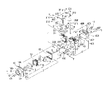
FIG. 1 is an exploded perspective view showing a camera assembly
structure according to an embodiment of the invention where an external
interface cable is led __________________________________________________
CA 02778180 2012-04-18
8
from a back face part of a housing;
FIG. 2 is a perspective view showing a part of the
camera assembly structure according to the embodiment,
where the external interface cable is led from a side
face part (upper face part/lower face part/left face
part/right face part) of the housing (an assembly
structure except a lens mount built-in module);
FIG. 3A is a side cross-sectional view showing the
camera assembly structure (assembled) shown in FIG. 1;
FIG. 3B is a perspective view showing a part of
the camera assembly structure (assembled) shown in
FIG. 1;
FIG. 4A is a side cross-sectional view showing the
camera assembly structure (assembled) shown in FIG. 2;
FIG. 4B is a perspective view showing a part of
the camera assembly structure (assembled) shown in
FIG. 2;
FIG. 5A is a perspective view showing a camera
assembly structure and a built-in state where the
external interface cable is led from a back face part
of the housing, according to the embodiment;
FIG. 5B is a perspective view showing an exterior
configuration of a camera assembly structure
(assembled) where the external interface cable is led
from the back face part of the housing, according to
the embodiment;
FIG. 6A is a perspective view showing a camera
CA 02778180 2012-04-18
9
assembly structure and a built-in state where the
external interface cable is led from an upper face part
of the housing, according to the embodiment;
FIG. 6B is a perspective view showing an exterior
configuration of a camera assembly structure
(assembled) where the external interface cable is led
from the upper face part of the housing, according to
the embodiment;
FIG. 7A is a perspective view showing a camera
assembly structure and a built-in state where the
external interface cable is led from a lower face part
of the housing, according to the embodiment;
FIG. 7B is a perspective view showing an exterior
configuration of a camera assembly structure
(assembled) where the external interface cable is led
from the lower face part of the housing, according to
the embodiment;
FIG. 8A is a perspective view showing a camera
assembly structure and a built-in state where the
external interface cable is led from a left face part
of the housing, according to the embodiment;
FIG. 8B is a perspective view showing an exterior
configuration of a camera assembly structure
(assembled) where the external interface cable is led
from the left face part of the housing, according to
the embodiment;
FIG. 9A is a perspective view showing a camera
CA 02778180 2012-04-18
assembly structure and a built-in state where the
external interface cable is led from a right face part
of the housing, according to the embodiment;
FIG. 9B is a perspective view showing an exterior
5 configuration of a camera assembly structure
(assembled) where the external interface cable is led
from the right face part of the housing, according to
the embodiment;
FIG. 10A is an exploded perspective view showing
10 for explaining an assembly procedure where the external
interface cable is led from a back face part of the
housing, according to the embodiment;
FIG. 10B is an exploded perspective view showing
for explaining the assembly procedure where the
external interface cable is led from the back face part
of the housing, according to the embodiment;
FIG. 11A is an exploded perspective view showing
for explaining the assembly procedure where the
external interface cable is led from the back face part
of the housing, according to the embodiment;
FIG. 11B is an exploded perspective view showing
for explaining the assembly procedure where the
external interface cable is led from the back face part
of the housing, according to the embodiment;
FIG. 12A is an exploded perspective view showing
for explaining the assembly procedure where the
external interface cable is led from the back face part
CA 02778180 2012-04-18
11
of the housing, according to the embodiment;
FIG. 12B is a perspective view showing an exterior
configuration of a camera assembly structure
(assembled) where the external interface cable is led
from the right face part of the housing, according to
the embodiment;
FIG. 13A is an exploded perspective view showing
for explaining an assembly procedure where the external
interface cable is led from a face part of the housing
(upper face part/lower face part/left face part/right
face part), according to the embodiment;
FIG. 13B is an exploded perspective view showing
for explaining the assembly procedure where the
external interface cable is led from the face part of
the housing (upper face part/lower face part/left face
part/right face part), according to the embodiment;
FIG. 14A is an exploded perspective view showing
for explaining the assembly procedure where the
external interface cable is led from the face part of
the housing, according to the embodiment;
FIG. 14B is an exploded perspective view showing
for explaining the assembly procedure where the
external interface cable is led from the face part of
the housing, according to the embodiment;
FIG. 15 is an exploded perspective view showing
for explaining the assembly procedure where the
external interface cable is led from the face part of
CA 02778180 2012-04-18
12
the housing, according to the embodiment;
FIG. 16 is a perspective view for schematically
explaining a POP board, according to the embodiment;
FIG. 17A is a perspective view showing a structure
of a main part of a POP board, according to the
embodiment; and
FIG. 17B is a side view showing another example
structure of the main part of the POP board, according
to the embodiment.
Description of Embodiments
Hereinafter, an embodiment of the invention will
be described with reference to the drawings.
FIGS. 1, 2, 3A, and 4A show a camera assembly
structure of a small industrial electronic imaging
camera according to an embodiment of the invention.
FIG. 1 (exploded perspective view) and FIG. 3A (side
cross-sectional view) show the assembly structure when
an external interface connector is provided at a back
face part (rear face part) of a box-type camera housing
having a hexahedral structure, to lead an external
interface cable from the back face part of the box-type
camera housing. FIG. 2 (partial exploded perspective
view) and FIG. 3A (side cross-sectional view) show an
assembly structure when an interface connector is
provided at an arbitrary side face part (any one of
upper, lower, left, and right face parts) of the box-
type camera housing, to lead an external interface
CA 02778180 2012-04-18
13
cable from the side face part of the box-type camera
housing. In the following, the camera assembly
structure shown in FIGS. 1 and 3A will be referred to
as a back cable lead assembly structure, and the camera
assembly structure shown in FIGS. 2 and 4A will be
referred to as a side cable lead assembly structure.
As shown in FIGS. 1, 2, 3A, and 4A, the small
industrial electronic imaging camera according to the
embodiment of the present invention comprises a lens
mount 10, a tri-face cover 30, a board mount frame 20,
a connector metal bracket 40, and an external
connection terminal 51. The lens mount 10 comprises an
imaging window 101 and forms a front face part of the
box-type camera housing 1 having a hexahedral
structure. The tri-face cover 30 having a rectangular
U-shaped cross-section can be attached to the lens
mount 10, with edges of the tri-face cover 30 switched
relatively to edges of the lens mount 10 around a
vertical axis parallel to an optical axis 01 of the
imaging window 101. The tri-face cover 30 forms
arbitrary three side faces or two side faces and a back
face of the camera housing 1. The board mount frame 20
comprises a board mount mechanism 205 which contains
and supports a plurality of boards in an imaging
chamber 2 formed in the camera housing 1. The board
mount frame 20 is attached to the lens mount 10 and
forms an arbitrary side face of the camera housing 1.
CA 02778180 2012-04-18
14
The connector metal bracket 40 is attached to the lens
mount 10 and thereby forms an arbitrary side face of
the camera housing 1 or a back face of the camera
housing 1. The external interface connector 50
comprises an external connection terminal 51 for
connecting an external interface cable, and is attached
with the connector metal bracket 40 with the external
connection terminal 51 exposed to outside.
The lens mount 10, the board mount frame 20, the
tri-face cover 30, and the connector metal bracket 40
attached with the external interface connector 50,
which are constitutive elements of the box-type camera
housing 1, are components forming the housing, which
are common to both the back cable lead assembly
structure and the side cable lead assembly structure.
The box-type camera housing 1 having a four-piece
structure according to the embodiment of the present
invention, in which an external interface connector can
be provided in an arbitrary face among five faces
except the front face, can be constructed by the lens
mount 10, board mount frame 20, the tri-face cover 30,
and the connector metal bracket 40 attached with the
external interface connector 50.
Between the back cable lead assembly structure
shown in FIGS. 1 and 3A and the side cable lead
assembly structure shown in FIGS. 2 and 4A, as is
apparent from comparison between the figures,
CA 02778180 2012-04-18
directions of an external connection terminal 502 led
from a connector terminal lead hole 403 are vertically
reversed to each other in relation to the connector
metal bracket 40 as shown in FIGS. 3B and 4B.
5 Accordingly, a direction of a terminal array of a
connection end surface 503 of an external connection
terminal 502 is reversed as well.
In the box-type camera housing 1 according to the
embodiment of the invention, a cable connection
10 direction of the external connection terminal 502
provided on the external interface connector 50 is
perpendicular to the optical axis 01 (i.e., a
connection end surface 503 of the external connection
terminal 502 is parallel to the optical axis 01), in
15 the back cable lead assembly structure in which the
connector metal bracket 40 forms the back face part of
the camera housing 1. In the side cable lead assembly
in which the connector metal bracket 40 forms any of
the right, left, upper, and lower face parts of the
camera housing 1, the cable connection direction of the
external connection terminal 502 is perpendicular to
the optical axis 01 (i.e., the connection end surface
503 of the external connection terminal 502 is parallel
to the optical axis 01).
In the back cable lead assembly structure in which
the connector metal bracket 40 forms the back face part
of the camera housing 1, the connector metal bracket 40
CA 02778180 2012-04-18
16
is fixed with screws to the lens mount 10 through the
board mount frame 20 and is also fixed with screws to
the lens mount 10 through the tri-face cover 30, as
shown in FIGS. 1 and 3A. In the side cable lead
assembly in which the connector metal bracket 40 forms
any of the right, left, upper, and lower face parts of
the camera housing 1, the connector metal bracket 40 is
fixed directly to the lens mount 10 and is fixed with
screws to the lens mount 10 through the tri-face cover
30 and board mount frame 20, as shown in FIGS. 2 and
4A. Screws T used for the fixing with screws are
partially omitted from the figures.
The lens mount 10 is configured to comprise a lens
frame part 102 and screw fixing pieces 104, 105, 106,
and 107. The lens frame part 102 is added with a top
mark 103 around an imaging window 101 in a face part
exposed to outside. The screw fixing pieces are
provided at corners on four edges of the back face
part, and each comprise two screw holes (threaded
holes) which are parallel to two edges perpendicular to
each other. The lens mount 10, the board mount frame
20, the tri-face cover 30, and the connector metal
bracket 40 attached with the external interface
connector 50 are fixed with screws to each other
through the eight screw holes in the fixing pieces 104,
105, 106, and 107. In this manner, the assembly
structures of the box-type camera housing 1 are formed
CA 02778180 2012-04-18
,
17
with the imaging chamber 2 formed therein. The top
mark 103 always clearly indicates up and down
directions of imaging planes (described later) of a
solid-state imaging element for the assembly
structures. The top mark 103 is cut in the lens frame
part 102.
The board mount frame 20 comprises two engaging
pieces 202 and 203, two screw fixing pieces 201 and
204, and a board fixing piece 205. The two engaging
pieces 202 and 203 each comprise a face part exposed to
outside where a nameplate is bonded, and comprise a
back face part where a screw insertion hole is cut.
Two screw fixing pieces 201 and 204 respectively
comprise screw holes (threaded holes). The board
fixing piece 205 forms the board mount mechanism. The
engaging piece 202 is provided at a corner on an edge a
in a side of an edge b, and the engaging piece 203 is
provided at a corner on an edge c in a side of the edge
b. Screw fixing holes are cut in a direction parallel
to the edge b in the engaging pieces 202 and 203. The
screw fixing piece 201 is provided at a corner on an
edge d in a side of the edge c. A screw hole in a
direction perpendicular to the edge a is cut in the
_
screw fixing piece 201, and a screw hole in a direction
perpendicular to the edge d is cut in the screw fixing
piece 204. The board fixing piece 205 is provided on
the edge a, and a screw hole is provided in a direction
CA 02778180 2012-04-18
18
parallel to the edge a.
The screw fixing piece 201 engages with a screw
fixing hole 315 in the tri-face cover 30 in the back
cable lead assembly structure, and engages with the
screw fixing hole 315 in the tri-face cover 30 in the
side cable lead assembly structure. The engaging piece
202 is fixed with screws to a screw fixing piece 107 in
the lens mount 10 in the back cable lead assembly
structure, and is fixed with screws to a screw fixing
piece 105 in the lens mount 10 in the side cable lead
assembly structure. The engaging piece 203 is fixed
with screws to a screw fixing piece 106 in the lens
mount 10 in the back cable lead assembly structure, and
is fixed with screws to a screw fixing piece 104 in the
lens mount 10 in the side cable lead assembly
structure. The screw fixing piece 204 engages with a
screw fixing hole 411 in the connector metal bracket 40
in the back cable lead assembly structure, and engages
with the screw fixing hole 315 in the tri-face cover 30
in the side cable lead assembly structure.
The tri-face cover 30 is formed of an intermediate
(or central) face part 301 and face parts 302 and 303
in two sides, to have a rectangular U-shaped cross
section. End edges of the rectangular U-shaped cross-
section at one end portion are in the same plane as
each other. Another end edge of the intermediate face
part 301 is protruded (extended) from the end edges of
CA 02778180 2012-04-18
19
the two sides. The protruded face part (extended part)
304 forms a cover of an extended part 402 (connector
container chamber 6) and a mount piece (a piece fixed
with screws to the connector metal bracket 40) of the
connector metal bracket 40.
The screw fixing hole 311 is cut at a corner of
the intermediate face part 301 of the tri-face cover 30
on one end edge in a side of the face part 303. Screw
fixing holes 312 and 313 are cut at two corners of the
intermediate face part 301 of the tri-face cover 30 on
another end edge. Of the face parts 302 and 303 in the
two sides, a screw fixing hole 314 is cut at a corner
of the face part 302 in a side of the face part 301,
and a screw fixing hole 315 is cut at an end of the
face part 303 in the side of the another end edge.
Termination ends of the face parts 302 and 303 in the
side of the one end edge in two sides of the tri-face
cover 30 form notch parts 316 and 317 which engage with
engaging pieces 202 and 203 provided on the board mount
frame 20.
The screw fixing hole 311 is fixed with a screw to
the screw fixing piece 104 in the lens mount 10 in the
back cable lead assembly structure, and is fixed with a
screw to the screw fixing piece 204 on the board mount
frame 20 in the side cable lead assembly structure.
The screw fixing holes 312 and 313 are fixed with
screws to the screw fixing pieces 406 and 407 on the
CA 02778180 2012-04-18
connector metal bracket 40. The screw fixing hole 314
is fixed with a screw to the screw fixing piece 105 on
the lens mount 10 in the back cable lead assembly
structure, and is fixed with a screw to the screw
5 fixing piece 201 on the board mount frame 20 in the
side cable lead assembly structure.
The connector metal bracket 40 comprises a mount
piece 401, and forms the connector container chamber 6
which contains a body part (connector body) 501 of the
10 external interface connector 50 in the extended part
402.
A screw fixing hole 411 is cut in the bracket
fixing piece 401. The screw fixing hole 411 is fixed
with a screw to the screw fixing piece 204 of the board
15 mount frame 20 in the back cable lead assembly
structure, and is fixed with a screw to any of the
screw fixing pieces 104, 105, 106, and 107 in the side
cable lead assembly structure. The extended part 402
extended from the bracket fixing piece 401 forms a
20 support frame part of a connector. The extended part
402 is provided with a connector terminal lead hole 403
in an extended face parallel to a mount face of the
bracket fixing piece 401, and leads the external
connection terminal 502 of the external interface
connector 50 to outside. Connector support parts 404
which engage with and support a connector body 501 are
provided in two sides of the connector terminal lead
CA 02778180 2012-04-18
,
' 21
hole 403. Screw fixing pieces 406 and 407 which fix,
with screws, the screw fixing holes 312 and 131
provided in a protruded face part 304 of the tri-face
cover 30 are provided in an extended end of the
extended part 402.
The external interface connector 50 is fixed to
the connector metal bracket 40 by a pair of clamp
screws 41 with lock terminals. The clamp screws 41
with lock terminals (terminals) each comprise a plug-
clamp lock terminal for fastening a plug (connector) to
the external connection terminal 502 when a connection
plug (connector) of an unillustrated external interface
cable is interface-connected to the external connection
terminal 502 of the external interface connector 50.
The external interface connector 50 forms a camera link
connector according to a camera link standard.
The imaging chamber 2 formed in the box-type
camera housing 1 having a four-piece structure as
described above contains a lens mount built-in module 3
which forms a sensor module, and a frame built-in
module 4 which forms a control module. A body part 501
of the external interface connector 50 is contained in
the connector container chamber 6 which communicates
with the imaging chamber 2 and is formed in the
extended part 402. The connector metal bracket 40 and
the external interface connector 50 attached to the
connector metal bracket 40 form a connector module 5.
CA 02778180 2012-04-18
22
The lens mount built-in module 3 which forms the
sensor module is comprised of a lens mount 10, an 0-
ring 11, a shim 12 for adjusting a flange back, a
solid-state imaging element 13, a device holder 14, and
a sensor board (rigid board) 15. The solid-state
imaging element 13 comprises a rectangular imaging
plane 13a, which forms an area image sensor. The
device holder 14 holds the solid-state imaging element
13. The sensor board (rigid board) 15 mounts the
solid-state imaging element 13 through the device
holder 14.
Among constitutive elements of the lens mount
built-in module 3, the solid-state imaging element 13
is a charge-coupled device (CCD) or complementary metal
oxide semiconductor (CMOS) image sensor. In the
present embodiment, the CCD is employed as the solid-
state imaging element 13, and the CCD 13 is mounted on
the sensor board 15 by the device holder 14. The CCD
13 is fixed to and supported on the sensor board 15
with its position adjusted by the shim 12 in a manner
that the rectangular imaging plane 13a is located at a
position where a flange back on the optical axis 01 is
maintained. The shim 12 for adjusting the flange back
is appropriately used upon necessity in optical
adjustment work, and is not equipped in some cases.
The flange back (FB) is determined by a distance
(flange focal length) to a focus (imaging plane 13a)
CA 02778180 2012-04-18
23
from, as a reference, an open end (flange face of a
lens) of the imaging window 101 provided on the lens
mount 10.
The lens mount built-in module 3 is configured by
fixing the sensor board 15, which mounts the CCD 13 by
the device holder 14, with screws to the lens mount 10,
with the ring 11 and shim 12 inserted therebetween and
with the device holder 14 used as a fixing/support
member.
The frame built-in module 4 which forms a control
module is comprised of the board mount frame 20, a
control board (rigid board) 21, and a power supply
board 22. The control board 21 and the power supply
board 22 are layered on each other, are physically
integrated by columnar solder balls SB (barrel-type
resin core solder balls), and are circuited and
connected to each other, forming a package-on-package
(POP) board having a double-board structure. The POP
board using the barrel-type resin core solder balls SB
will be described later with reference to FIGS. 16,
17A, and 17B.
The POP board comprised of the control board 21
and the power supply board 22 is fixed with a screw to
the board fixing piece 205, and is supported by and
fixed to the board mount frame 20, with the control
board 21 and power supply board 22 standing on a
surface of the board mount frame 20. In this manner,
CA 02778180 2012-04-18
24
the frame built-in module 4 forming the control module
is constructed.
The connector module 5 and the frame built-in
module 4 as described above are circuited to each other
to be connectable and disconnectable through a
connector by a connector-connection flexible printed
wiring board (external interface flexible printed
wiring board) 23. The frame built-in module 4 and lens
mount built-in module 3 are circuited to each other to
be connectable and disconnectable through a connector
by a sensor circuit flexible printed wiring board 25.
The external interface flexible printed wiring board 23
comprises an IC component 24 provided thereon for
signal processing. The sensor circuit flexible printed
wiring board 25 has a length which allows the frame
built-in module 4 and connector module 5 to be folded
multiple times to the lens mount built-in module 3,
pivotally about a vertical axis parallel to the optical
axis 01.
FIGS. 5A, 5B, 6A, 6B, 7A, 7B, 8A, 8B, 9A, and 9B
show built-in states of the back cable lead assembly
structure and the camera assembly structure, and
exterior configurations before and after building the
structures in the camera assembly structures described
above.
FIG. 5A shows a built-in state in which the
connector module 5 is provided on the back face (rear
CA 02778180 2012-04-18
face) part of the box-type camera housing 1. FIG. 5B
shows an exterior configuration thereof after being
built in. In this assembly structure (in the case of
an assembly structure in which an external interface
5 cable is led from the back face part), the board mount
frame 20 forms a bottom part of the camera housing 1.
FIG. 6A shows a built-in state in which the
connector module 5 is provided on the top face (rear
face) part of the box-type camera housing 1. FIG. 6B
10 shows an exterior configuration thereof after being
built in. In this assembly structure (in the case of
an assembly structure in which an external interface
cable is led from the top), the board mount frame 20
forms the bottom part of the camera housing 1, as in
15 the assembly structure shown in FIGS. SA and 5B.
FIG. 7A shows a built-in state in which the
connector module 5 is provided on a lower face part of
the box-type camera housing 1. FIG. 7B shows an
exterior configuration thereof after being built in.
20 In this assembly structure (in the case of an assembly
structure in which an external interface cable is led
from the lower face), the board mount frame 20 forms
the top part of the camera housing 1.
FIG. 8A shows a built-in state in which the
25 connector module 5 is provided on a left side face part
of the box-type camera housing 1. FIG. 8B shows an
exterior configuration thereof after being built in.
CA 02778180 2012-04-18
26
In this assembly structure (in the case of an assembly
structure in which an external interface cable is led
from a left side face), the board mount frame 20 forms
a right side face part of the camera housing 1.
FIG. 9A shows a built-in state in which the
connector module 5 is provided on a right side face
part of the box-type camera housing 1. FIG. 9B shows
an exterior configuration thereof after being built in.
In this assembly structure (in the case of an assembly
structure in which an external interface cable is led
from a right side face), the board mount frame 20 forms
a left face part of the camera housing 1.
FIGS. 10A, 10B, 11A, 11B, 12A, and 12B show an
assembly procedure for assembling the back cable lead
assembly structure described above. FIGS. 13A, 13B,
14A, 14B, 15A, and 15B show an assembly procedure for
assembling the side cable lead assembly structure.
In the assembly procedure for assembling the back
cable lead assembly structure, cushion materials C5 are
bonded to two surfaces of the IC component 24 mounted
on the external interface flexible printed wiring board
23, as shown in FIG. 10A. Thereafter, the external
connection terminal 502 of the external interface
connector 50 to which the external interface flexible
printed wiring board 23 is soldered is led to outside
of the connector container chamber 6 through the
connector terminal lead hole 403 of the connector metal
CA 02778180 2012-04-18
27
bracket 40. The external interface connector 50 is
fixed to the connector metal bracket 40 by the clamp
screws 41 with the lock terminals, thereby forming the
connector module 5. Further, as shown in FIG. 10B, the
external interface flexible printed wiring board 23 is
connected by a connector to the control board 21 of the
frame built-in module 4.
Subsequently, the external interface flexible
printed wiring board 23 to which the frame built-in
module 4 and connector module 5 are circuited and
connected is folded as shown in FIGS. 11A and 11B, and
the connector metal bracket 40 is engaged with the
board mount frame 20. Thereafter, as shown in
FIG. 12A, the lens mount built-in module 3 is built in
the frame built-in module 4. The tri-face cover 30 is
fixed with screws to the lens mount built-in module 3,
frame built-in module 4, and connector module 5, with
the cushion materials Cl, C2 inserted. In a step of
building the lens mount built-in module 3 into the
frame built-in module 4, the sensor circuit flexible
printed wiring board 25 is folded and contained between
the sensor board 15 and the control board 21, as shown
in FIGS. 3A and 5A.
In this manner, the small industrial electronic
imaging camera having the back cable lead assembly
structure as shown in FIG. 12B is constructed (see
FIG. 5B).
CA 02778180 2012-04-18
28
In the assembly procedure for assembling the side
cable lead assembly structure, as shown in FIG. 13A,
the external connection terminal 502 of the external
interface connector 50 to which the external interface
flexible printed wiring board 23 is soldered is led to
outside of the connector container chamber 6 through
the connector terminal lead hole 403. The external
interface connector 50 is fixed with the clamp screws
41 with lock terminals to the connector metal bracket
40, thereby forming the connector module 5. Between
the side cable lead assembly structure and the back
cable lead assembly structure, directions of the
external connection terminal 502 to be inserted into
the connector terminal lead hole 403 are vertically
reversed to each other in relation to the connector
terminal lead hole 403. Further, as shown in FIG. 13B,
the external interface flexible printed wiring board 23
led from the connector module 5 is connected by a
connector to the control board 21 of the frame built-in
module 4, and cushion materials C4 are bonded to the
power supply board 22.
Subsequently, the external interface flexible
printed wiring board 23, which circuits and connects
the frame built-in module 4 and connector module 5, is
folded as shown in FIGS. 14A and 143. As shown in
FIG. 15, the lens mount built-in module 3 is built in
the frame built-in module 4. The tri-face cover 30 is
CA 02778180 2012-04-18
,
,
29
fixed with screws to the lens mount built-in module 3,
frame built-in module 4, and connector module 5. In
this assembly step, depending on which of right, left,
upper, and lower side faces of the camera housing 1 the
external interface connector 50 is to be provided on,
the frame built-in module 4 is pivoted in units of 90
degrees about a vertical axis parallel to the optical
axis 01 (see an arrow direction r in the figure), to
form a desired side cable lead assembly structure. In
this case, the sensor circuit flexible printed wiring
board 25 has a length which allows the board 25 to be
folded multiple times. With the lens mount built-in
module 3 and frame built-in module 4 circuited and
connected, the cable lead direction of the camera
housing 1 can be arbitrarily changed to any of the
right, left, upper, and lower side faces.
On a surface of the board mount frame 20 forming a
face part of the camera housing 1, the control board 21
and power supply board 22 are supported to stand as the
POP board. In any of the back cable lead assembly
structure and side cable lead assembly structure, the
POP board described above is mounted in the same array
as the sensor board 15 built in the lens mount built-in
module 3 in a manner that these boards are layered on
each other. Therefore, a board mount space for the
imaging chamber 2 can be suppressed to minimum.
Further, a structure of the POP board is
CA 02778180 2012-04-18
configured to be robust against thermal deformation and
pressure deformation by using barrel-type resin core
solder balls SB, without connecting the control board
21 and power supply board 22 by a connector. In this
5 manner, a circuit connection is achieved, maintaining
the control board 21 and power supply board 22 stable
for a long period, and the boards are integrated
rigidly at a set constant gap.
The sensor board 15, control board 21, and power
10 supply board 22 can be mounted in the imaging chamber 2
of the microcamera housing 1 of an approximately 20 mm
cube by a same-array mount means for mounting the
sensor board 15 and POP board in the same array in both
of the back cable lead assembly structure and side
15 cable lead assembly structure, and by the POP board
structure using the barrel-type resin core solder balls
SB.
FIGS. 16 and 17A show the POP board structure of
the control board 21 and power supply board 22, which
20 uses the barrel-type resin core solder balls. In the
control board 21, an active circuit component P1 which
generates heat during operation is mounted on a board
face of the control board 21, which is opposed to the
power supply board 22. On a pattern forming face of
25 the power supply board 22 which is opposed to the
control board 21, barrel-type resin core solder balls
SB are arrayed on both sides of a face part opposed to
CA 02778180 2012-04-18
31
the active circuit component Pl, avoiding the surface
part facing with the active circuit component Pl. The
power supply board 22 and control board 21 are soldered
to each other by a solder re-flow processing. In this
manner, the control board 21 and power supply board 22
are integrated and circuited to each other by the
barrel-type resin core solder balls SB, with the solder
balls SB arrayed on both sides of the active circuit
component P1 mounted on the control board 21. Thus,
the POP board having a double-board structure is
manufactured. P2 shown in FIG. 17A denotes circuit
components mounted on a component mount face of the
control board 21, and P3 denotes circuit components
mounted on a component mount face of the power supply
board 22.
In the POP board having a double-board structure
configured by the control board 21 and power supply
board 22, barrel-type resin core solder balls SB are
arrayed on both sides of the active circuit component
Pl. A gap (hr) can be formed at a constant clearance
(gb) by setting a greater dimension (ga) of the barrel-
type resin core solder balls SB in a height direction
vertical to the board face than a height of the mounted
active circuit component Pl. In an actual device,
barrel-type resin core solder balls SB having ga =-
1.5 mm are used to form the gap (hr) having gb
0.3 mm. The gap (hr) contributes to forming of a waste
CA 02778180 2012-04-18
32
heat path which guides heat generated from the active
circuit component P1 to the barrel-type resin core
solder balls SB arrayed on both sides of the active
circuit component Pl.
FIG. 17B shows the POP board structure when active
circuit components each of which generates heat during
operation are mounted on the mutually opposed faces of
the control board 21 and power supply board 22. Here,
an active circuit component Pa is mounted on the
control board 21 and a circuit component Pb is mounted
on the power supply board 22. In this case, the
dimension (ga) of the barrel-type resin core solder
balls SB in the direction vertical to the board face is
set to be a greater value than a total of actual
heights of the active circuit component Pa and circuit
component Pc. A gap (hr) of a constant clearance (gd)
can be thereby formed between upper faces of the active
circuit component Pa and circuit component Pc. Pb
shown in FIG. 17B denotes circuit components mounted on
a component mount face of the control board 21, Pd
denotes circuit components mounted on a component mount
face of the power supply board 22, and gb denotes a gap
formed between the upper face of the active circuit
component Pa and the board face of the power supply
board 22. go denotes a gap formed between the upper
face of the circuit component Pc and the board face of
the control board 21.
CA 02778180 2012-04-18
33
As has been described above, according to the
embodiment of the invention, a mount face for an
external interface connector can be set and changed to
an arbitrary face (back face, right side face, left
side face, upper side face, or lower side face) among
five faces of a box-type camera housing except a front
face part (lens mount) thereof. In this manner, an
external interface cable from the camera housing can be
led in an arbitrary direction among five directions as
targets, i.e., a back leading direction parallel to an
optical axis of the camera, a right, left, upper, and
lower leading perpendicular to the optical axis of the
camera. In this manner, there is provided a small
industrial electronic imaging camera comprising a
connection mechanism for an external interface cable
with high general versatility, wherein the camera can
be easily assembled with a leading direction of the
external interface cable arbitrarily selected, in an
economically advantageous configuration.
Also, there is provided a small industrial
electronic imaging camera which can integrate camera
functions by containing, in an imaging chamber in a
camera housing, a control board for controlling a
sensor board, and a power supply board for supplying
and controlling an operation power for the sensor board
and control board, and can be expected to achieve
highly reliable circuit operation.
CA 02778180 2012-04-18
34
The present invention is not limited just to the
embodiment described above but various camera assembly
structures can be achieved by modifying constitutive
elements without deviating from the spirit of the
invention.
Reference Signs List
1_ Camera housing, 2_ Imaging chamber, 3_ Lens mount
built-in module, 4_ frame built-in module, 5_ Connector
module, 6_ Connector container chamber, 10_ Lens mount,
11_ 0-ring, 12_ Shim, 13_ Solid-state imaging device
(CCD), 14_ Device holder, 15_ Sensor board, 20_ Board
mount frame, 21_ Control board, 22_ Power supply board,
23_ External interface flexible printed wiring board,
24_ IC component, 25_ Sensor circuit flexible printed
wiring board, 30_ Tr-face cover, 40_ Connector metal
bracket, 41_ Clamp screw with lock terminal, 50_
External interface connector, 101_ Imaging window, 102_
Lens frame part, 103_ Top mark, 401_ Bracket fixing
piece, 402_ Extended part, 403_ Connector terminal lead
hole, 501_ Body part (connector body), 502_ External
connection terminal, 503_ Connection end surface, 01_
Optical axis, SB_ Columnar resin core solder ball
having a swollen center part (barrel-type resin core
solder ball)