Note : Les descriptions sont présentées dans la langue officielle dans laquelle elles ont été soumises.
CA 02779373 2015-11-16
USER INTERFACE PANEL
[0001]
BACKGROUND OF THE INVENTION
[0002] The present invention is directed to a user interface panel using
electronic sensor
technology.
BRIEF DESCRIPTION OF THE DRAWINGS
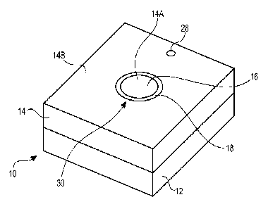
[0003] FIG. 1 is a perspective view of a user interface panel 10 including
a circuit
carrier substrate 12 and a user interface substrate 14 defining a touch
surface 16, a gap 18
surrounding touch surface 16, and an indicator 28;
[0004] FIG. 2A is a plan view of user interface substrate 14 defining a
round touch
surface 16, a gap 18 surrounding touch surface 16, and an indicator 28;
[0005] FIG. 2B is a plan view of user interface substrate 14 defining a
square touch
surface 16, a gap 18 surrounding touch surface 16, and an indicator 28;
[0006] FIG. 3A is a plan view of circuit carrier substrate 12 having a
touch sensor 20
disposed thereon, touch sensor 20 including a generally round, conductive
electrode pad 22
and a narrow, conductive electrode 24 substantially surrounding electrode pad
22;
1
CA 02779373 2012-04-27
WO 2011/063377
PCT/US2010/057734
[0007] FIG. 3B is a plan view of circuit carrier substrate 12 having a
touch sensor 20
disposed thereon, touch sensor 20 including a generally square, conductive
electrode pad 22
and a narrow, conductive electrode 24 substantially surrounding electrode pad
22;
[0008] FIG. 3C is a plan view of circuit carrier substrate 12 having a
touch sensor 20
disposed thereon, touch sensor 20 including a generally square, conductive
electrode pad 22
and a narrow, conductive electrode 24 abutting one side of electrode pad 22;
[0009] FIG. 4A is a plan view similar to FIG. 2A showing electrode pad 22
and electrode
24 in phantom;
[0010] FIG. 4B is a plan view similar to FIG. 2B showing electrode pad 22
and electrode
24 in phantom;
[0011] FIG. 5 is a cross-sectional view of user interface panel 10
including circuit carrier
substrate 12 having touch sensor 20 disposed thereon and user interface
substrate 14 defining
touch surface 16 and gap 18 surrounding touch surface 16;
[0012] FIG. 6 is a plan view of an interface panel 10 having a generally
round touch
surface 16, a generally annular gap 18, and a touch sensor 20, shown in
phantom, having a
generally square electrode 22 pad and a generally square annular electrode 24
substantially
surrounding electrode pad 22;
[0013] FIG. 7 is a perspective view of a user interface panel 10 including
a circuit carrier
substrate 12 and a user interface substrate 14 that defines a plurality of
touch surfaces 16 and
gaps 18 surrounding touch surfaces 16;
[0014] FIG. 8 is a plan view of an alternative structure for electrode pad
22;
[0015] FIG. 9 is a plan view of a portion of user interface substrate 14
defining touch
surface 16;
2
CA 02779373 2012-04-27
WO 2011/063377 PCT/US2010/057734
[0016] FIG. 10 is a plan view of a portion of user interface substrate 14
defining touch
surface 16;
[0017] FIG. 11 is a plan view of a portion of user interface substrate 14
defining touch
surface 16;
[0018] FIG. 12 is a plan view of a user interface panel 10 having an
alternate form of user
interface substrate 14; and
[0019] FIG. 13 is a plan view of a user interface panel 10 having another
alternate form of
user interface substrate 14.
DETAILED DESCRIPTION OF THE ILLUSTRATED EMBODIMENTS
[0020] FIGS. 1-11 illustrate several exemplary embodiments of a user
interface panel 10
including a circuit carrier substrate 12, a touch sensor 20 disposed on a
first surface of circuit
carrier substrate 12, and a user interface substrate 14 disposed on a second
surface of circuit
carrier substrate 12. User interface substrate 14 defines a touch surface 16
and a gap 18
surrounding touch surface 16.
[0021] Circuit carrier substrate 12 can be embodied as any rigid or
flexible substrate
suitable for carrying touch sensors, electrical circuitry, conductive traces,
and/or electrical
components. For example, circuit carrier substrate 12 can be embodied as a
rigid printed
wiring board made of FR4 material or a flexible carrier comprising a polyester
or Mylar sheet.
If embodied as a flexible carrier, circuit carrier substrate 12 preferably,
but not necessarily, is
attached to a further, rigid substrate. One skilled in the art would recognize
that circuit carrier
substrate 12 could be embodied in many other forms, as well. For example,
circuit carrier
substrate 12 could be embodied as a piece of glass, plastic, or other suitable
material.
3
CA 02779373 2012-04-27
WO 2011/063377 PCT/US2010/057734
Preferably, circuit carrier substrate 12 does not include, at least in the
proximity of touch sensor
20 as described further below, any perforations, apertures or other means
enabling liquids or
other contaminants to pass through circuit carrier substrate 12, from one side
thereof to the
other.
[0022] Touch sensor 20 includes a first electrode 22 in the form of a
conductive, inner
electrode pad and a relatively narrow, second, outer electrode 24 adjacent at
least a portion of
first sensing electrode. Preferably, second sensing electrode 24 is spaced
from and
substantially surrounds first electrode 22, as shown in FIGS. 3A and 3B. In
alternate
embodiments, second sensing electrode 24 could be spaced from and adjacent
only a portion of
first sensing electrode 22, as shown in FIG. 3C.
[0023] FIGS. 3A and 3B illustrate first electrode 22 as having a solid
geometric form. In
other embodiments, first electrode 22 could have a substantially open, for
example, annular or
grid-like, geometric form and/or second electrode 24 could partially surround
first electrode 22.
Fig. 8 illustrates a first electrode 22 having a grid-like form and a second
electrode 24
substantially surrounding first electrode 22. In alternate embodiments, second
sensing
electrode 24 could be spaced from and adjacent only a portion of first sensing
electrode 22,
rather than substantially surrounding first sensing electrode 22, as shown in
FIG. 14.
[0024] FIGS. 3A and 4A illustrate first electrode 22 as generally round and
second
electrode 24 as generally annular. FIGS. 3B and 4B illustrate first electrode
22 as generally
square and second electrode 24 as generally square annular. In other
embodiments, first
electrode 22 could have other shapes, for example, generally rectangular or
irregular, and it
could be of substantially open, rather than solid, form. In such embodiments,
second electrode
4
CA 02779373 2015-11-16
24 could be formed to substantially or partially surround first electrode 22
and have a
complementary or other shape.
[0025] First and second electrodes 22, 24 can be made of any suitable
material and
disposed on circuit carrier substrate 12 using any suitable technique, as
would be recognized
by one skilled in the art. Suitable materials include, without limitation,
copper, silver, ITO,
and other conductive and semi-conductive materials, as would be understood by
one skilled
in the art. Suitable techniques include, without limitation, plating/etching
and screen
printing, as would be understood by one skilled in the art.
[0026] Touch sensor 20 can include one or more active components, for
example,
transistors, disposed on circuit carrier substrate 12 proximate first and
second electrodes 22,
24 and coupled thereto, as described in U.S. Patent Nos. 5,594,222 and
6,310,611 assigned
to TouchSensor Technologies, LLC. Alternatively, touch sensor 20 can include
an integral
field generation and detection circuit disposed on circuit carrier substrate
12 proximate first
and second electrodes 22, 24 and coupled thereto, as described in U.S. Patent
No. 6,320,282
assigned to TouchSensor Technologies, LLC. The foregoing sensors sometimes are
referred
to as field effect sensors.
[0027] One or more electrical traces 26 can be disposed on circuit carrier
substrate 12.
Such traces can, for example, couple touch sensor 20 to one or more associated
controlled
devices, control circuits, or elements thereof, which can be located near to
or relatively far
from sensors 14. Such electrical traces can be disposed on circuit carrier
substrate 12 using
any suitable technique, as would be recognized by one skilled in the art.
CA 02779373 2012-04-27
WO 2011/063377 PCT/US2010/057734
[0028] User interface substrate 14 can be made of metal or other conductive
material. For
example, user interface substrate 14 can be embodied as a sheet of stainless
steel, copper,
aluminum, or other metal. Alternatively, user interface substrate 14 could be
embodied as a
plastic, glass or other substrate having a surface which is plated, coated, or
otherwise partially
or completely covered with a metal, for example, stainless steel, copper or
aluminum, or other
conductive material. Preferably, such surface is oriented outwardly so as to
be visible to and/or
touchable by a user. In either embodiment, the outward facing surface of user
interface
substrate 14 could bear a protective coating, for example, a lacquer coating.
Such a coating
could protect the surface from the environment, thereby inhibiting corrosion
and simplify
cleaning thereof. The coating could, but need not, act as an insulator.
Preferably, the coating
would be transparent so that the metal or conductive surface of user interface
substrate 14 is
visible there through.
[0029] User interface substrate 14 can be joined to circuit carrier
substrate 12 using any
suitable technique. For example, user interface substrate 14 can be joined to
circuit carrier
substrate 12 using adhesives, mechanical fasteners, and otherwise, as would be
recognized by
one skilled in the art. Preferably, user interface substrate 14 is joined to
circuit carrier substrate
12 so as to minimize or eliminate any air gap between the two, at least in the
proximity of first
sensing electrode 22 and second sensing electrode 24 and the electric fields
generated about
them, as discussed further below.
[0030] User interface substrate 14 is shown in FIG. 5 as being disposed on
a surface of
circuit carrier substrate 12 opposite the surface on which touch sensors 20
and other circuitry
and circuit components are located. In other embodiments, user interface
substrate 14 can be
disposed on the same side of circuit carrier substrate 12 as touch sensors 20
and/or other
6
CA 02779373 2012-04-27
WO 2011/063377 PCT/US2010/057734
conductive circuitry and/or circuit components, provided that some form of
electrical insulation
is provided between conductive portions of user interface substrate 14 and
such electrical
components. Such insulation could be embodied as a discrete insulating layer
or a portion of
user interface substrate 14 having suitable qualities as an electrical
insulator. For example, user
interface substrate 14 could be embodied as a plastic substrate with a
metalized user interface
surface, with the plastic portion acting as an insulator between the metalized
surface and such
electrical components.
[0031] User interface substrate 14 (or, in embodiments wherein user
interface substrate 14
is a non-conductive substrate with a metal or other conductive coating or
overlay, the
conductive surface thereof) includes a center portion 14A and a surrounding
portion 14B that
together define gap 18 between center portion 14A and surrounding portion 14B.
In essence,
surrounding portion 14B defines an aperture 30 in user interface substrate 14
or the conductive
portion thereof, part of which is occupied by center portion 14A. Aperture 30
and center
portion 14A are illustrated as being circular, but can take other shapes as
well. For example,
aperture 30 and center portion 14A can have generally rectangular, round, or
other regular or
irregular shapes. Aperture 30 and center portion 14A can, but need not, have
complementary
shapes. Consequently, gap 18 could, but need not, have a uniform width. The
exposed surface
of center portion 14A defines touch surface 16.
[0032] FIGS. 1, 2A, 2B, 4A, 4B, 6 and 7 illustrate center portion 14A as
having a generally
solid geometric form. In other embodiments, center portion 14A could have a
more open
geometric form. For example, as shown in FIGS. 9-11, center portion 14A could
include one
or more apertures or perforations 32 therein. Apertures 32 could have any
desired shape, and
could be provided for decorative and/or functional purposes. For example, as
shown in FIG.
7
CA 02779373 2012-04-27
WO 2011/063377 PCT/US2010/057734
11, apertures 32 could form text representing the function controlled by the
corresponding
touch sensor. Apertures 32 could form other text, as well. Backlighting could
be provided to
illuminate apertures 32 independently from gap 18 to further identify the
location of the
corresponding touch sensor, to indicate the status of a corresponding
controlled device, or
otherwise. For example, in the FIG. 11 embodiment, apertures 32 could be
backlit at a first
intensity or in a first color to identify the location of the corresponding
touch sensor and be
backlit at a second intensity or in a second color to indicate that the
corresponding controlled
device is in the "ON" state.
[0033] Center portion 14A overlies at least a portion of first electrode 22
of touch sensor
20. In the embodiments illustrated in FIGS. 4A and 4B (which are not drawn to
scale), center
portion 14A completely overlies first electrode 22. In the embodiment
illustrated in FIG. 6,
center portion 14A overlies most of first electrode 22. In other embodiments,
center portion
14a could overlie half or less of first electrode 22.
[0034] In the foregoing embodiments, center portion 14A does not overlie
second electrode
24 or the area between first electrode 22 and second electrode 24. In other
embodiments,
center portion 14A could overlie a relatively small portion of second
electrode 24 and the area
between first electrode 22 and second electrode 24. In further embodiments,
center portion
14A could overlie a larger portion, or substantially all, of second electrode
24.
[0035] In the embodiments illustrated in FIGS. 4A and 4B, surrounding
portion 14B
surrounds second electrode 24 such that no portion of surrounding portion 14B
overlies second
electrode 24. In some embodiments, for example, the embodiment illustrated in
FIG. 6,
surrounding portion 14B can overlie a relatively small portion of second
electrode 24. In other
embodiments, surrounding portion 14B could overlie more or substantially all
of second
8
CA 02779373 2012-04-27
WO 2011/063377 PCT/US2010/057734
electrode 24. Preferably, surrounding portion 14B would not overlie any
portion of first
electrode 22.
[0036] Aperture 30, center portion 14B, and gap 18 can, but need not, have
shapes
complementary to those of touch sensor 20, first electrode 22, and second
electrode 24,
respectively. For example, FIGS. 2A, 3A and 4A illustrate embodiments wherein
first
electrode 22 and second electrode 24 have generally round and annular shapes,
respectively,
which are complementary to the generally round and annular shapes of center
portion 14A and
gap 18, respectively. Also, FIGS. 2B, 3B and 4B illustrate embodiments wherein
first
electrode 22 and second electrode 24 have generally square and square annular
shapes,
respectively, which are complementary to the generally square and square
annular shapes of
center portion 14A and gap 18. FIG. 6, on the other hand, illustrates an
embodiment wherein
first electrode 22 and second electrode 24 have generally square and square
annular shapes,
respectively, which are not complementary to the generally round and annular
shapes of center
portion 14A and gap 18.
[0037] As suggested above, gap 18 can, but need not, completely overlie
second electrode
24 such that the entirety of second electrode 24 would be visible through gap
18 but for any
intervening structure, for example, circuit carrier substrate 12 on which
second electrode 24 is
disposed. For example, in the embodiments illustrated in FIGS. 2A, 3A and 4A,
and in FIGS.
2B, 3B and 4B, gap 18 completely overlies second electrode 24. On the other
hand, in the
embodiment shown in FIG. 6, gap 18 does not completely overlie second
electrode 24. In
further embodiments, other portions or even the entirety of second electrode
24 could be
obscured by center portion 14A or surrounding portion 14B of user interface
substrate 14 (or
9
CA 02779373 2012-04-27
WO 2011/063377 PCT/US2010/057734
the metal or otherwise conductive surface thereof). For example, center
portion 14A or
surrounding portion 14B could overlie the entirety of second electrode 24.
[0038] In the illustrated embodiments, gap 18 completely overlies second
electrode 24
where center portion 14A, gap 18, first electrode 22 and second electrode 24
have
complementary shapes, and gap 18 does not completely overlie second electrode
24 where gap
18, first electrode 22 and second electrode 24 do not have complementary
shapes. In other
embodiments wherein gap 18, first electrode 22 and second electrode 24 have
complementary
shapes, gap 18 could only partially overlie second electrode 24. In further
embodiments where
two or more of gap 18, first electrode 22 and second electrode do not have
complementary
shapes, gap 18 could completely overlie second electrode 24. In still other
embodiments, gap
18 could overlie no portion of second electrode 24.
[0039] User interface 10 can, but need not, include an indicator to
indicate, for example, the
status of touch sensor 20 or the status of a controlled device coupled to
touch sensor 20. Such
an indicator can be embodied as an aperture 28 in user interface substrate 14
and any suitable
means for backlighting aperture 28, for example a lamp, LED, or other suitable
light source,
with or without a suitable reflector, as would be recognized by one skilled in
the art.
[0040] User interface 10 can, but need not, include means for illuminating
gap 18. For
example, a lamp, LED, or other suitable light source, with or without a
suitable reflector, can
be used to backlight gap 18, as would be recognized by one skilled in the art.
Such lighting
structures and/or associated power and control circuitry could be located on a
side of circuit
carrier substrate 12 away from user interface substrate 14. Alternatively,
such lighting
structures and/or associated power and control circuitry could be located on a
separate substrate
attached to or otherwise associated with a side of circuit carrier substrate
12 away from user
CA 02779373 2012-04-27
WO 2011/063377
PCT/US2010/057734
interface substrate 14. In such embodiments, at least relevant portions of
circuit carrier
substrate 12 would need to be sufficiently transparent or translucent to allow
light to pass
toward gap 18.
[0041] In
other embodiments, front-lighting could be provided using light pipe structure
located between circuit carrier substrate 12 and the user interface substrate
14 and one or more
associated light sources, for example, lamps or LEDs. In embodiments wherein
user interface
substrate 14 is a plastic, glass, or other substrate plated, coated or
otherwise covered with a
metal or other conductive material, the substrate material itself could be
used to conduct light
provided by a light source. For example, an LED could protrude into user
interface substrate
14 from circuit carrier substrate 12 or elsewhere, thereby providing light to
illuminate
transparent or translucent portions of user interface substrate 14.
[0042] FIGS.
1-6 illustrate user interface panels 10 having a single touch sensor 20 and
touch surface 16. In other embodiments, a user interface panel 10 can include
more than one
touch sensor 20 and touch surface 16. FIG. 7 illustrates a user interface
panel 10 having four
touch sensors 20 and touch surfaces 16. In other embodiments, a user interface
panel 10 could
have more or fewer than four touch sensors 20 and touch surfaces 16.
[0043] In
operation, a field generation circuit associated with touch sensor 20
generates
electric fields about first and second electrodes 22, 24. At least a portion
of the electric field
generated about first electrode 22 couples with center portion 14A. At least a
portion of the
electric field generated about second electrode 24 penetrates user interface
substrate 14 through
gap 18. The electric field generated about second electrode 24 tends to
preclude the electric
field generated about first electrode 22 from coupling to surrounding portion
14B.
11
CA 02779373 2012-04-27
WO 2011/063377 PCT/US2010/057734
[0044] A detection circuit associated with touch sensor 20 can detect
disturbances to the
foregoing electric fields resulting from the proximity of a stimulus, for
example, a finger or
other conductive object, to touch surface 16 and/or gap 18, and can
distinguish whether such
stimulus is proximate touch surface 16, gap 18, or both, based on disturbances
to the electric
fields caused by such stimulus. The detection circuit can be configured to
output a signal (or
lack thereof) indicative of a touch to touch surface 16 when a stimulus is
proximate only touch
surface 16. The field detection circuit also can be configured to output a
signal (or lack
thereof) indicative of no touch to touch surface 16 when no stimulus is
present proximate touch
surface 16, when a stimulus is simultaneously present proximate touch surface
16 and gap 18 or
when a stimulus is present proximate gap 18 but not touch surface 16.
[0045] In alternative embodiments, second electrode 24 could be omitted. In
such
embodiments, first electrode 22 preferably, but not necessarily, is fully
contained underneath
center portion 14A such that gap 18 precludes or limits coupling of the
electric field generated
about first electrode 22 to surrounding portion 14B. In such embodiments,
touch sensor 20
could be configured to output a signal (or lack thereof) indicative of a touch
to touch surface 16
when a stimulus is present proximate touch surface 16, regardless of whether
the stimulus also
is present proximate gap 18, and to output a signal (or lack thereof)
indicative of no touch to
touch surface 16 when a stimulus is not present proximate touch surface 16.
[0046] In other alternative embodiments, center portion 14A could be
omitted. In such
embodiments, touch surface 16 is defined by the structure underlying omitted
center portion
14A, as shown in FIG. 13. This structure could be, for example, an exposed
surface of circuit
carrier substrate 12 or, where user interface substrate 14 is embodied as a
non-conductive
substrate bearing a conductive coating, a portion of the non-conductive
substrate 14.
12
CA 02779373 2012-04-27
WO 2011/063377 PCT/US2010/057734
[0047] In such embodiments, both first electrode 22 and second electrode 24
preferably lie
within the confines of aperture 30 such that the electric fields generated
about first electrode 22
and second electrode 24, or portions thereof, penetrate user interface
substrate 14 through
aperture 30. The detection circuit detects disturbances to the electric fields
caused by a
stimulus in proximity thereto. The detection circuit could be configured to
output a signal (or
lack thereof) indicative of a touch to touch surface 16 when a stimulus is
proximate only the
portion of touch surface 16 overlying first electrode 22. The field detection
circuit also can be
configured to output a signal (or lack thereof) indicative of no touch to
touch surface 16 when
no stimulus is present proximate touch surface 16, when a stimulus is
simultaneously present
proximate the portion of touch surface 16 overlying first electrode 22 and
second electrode 24,
or when a stimulus is present proximate the portion of touch surface 16
overlying second
electrode 24 but not the portion of touch surface 16 overlying first electrode
22.
[0048] Alternatively, surrounding portion 14B could overlie some portion or
all of second
electrode 24, or it could overlie all of second electrode 24 and a portion of
first electrode 22. In
such embodiments, at least a portion of the electric field generated about
first electrode 22
would penetrate user interface surface 14 through aperture 30 and at least a
portion of the
electric field generated about second electrode 24 could couple to surrounding
portion 14B. In
such embodiments, the detection circuit could be configured to output a signal
(or lack thereof)
indicative of a touch to touch surface 16 when a stimulus is proximate only
touch surface 16
and to output a signal (or lack thereof) indicative of no touch to touch
surface 16 when no
stimulus is present proximate touch surface 16, when a stimulus is
simultaneously present
proximate touch surface 16 and neighboring portions of surrounding portion
14B, or when a
13
CA 02779373 2012-04-27
WO 2011/063377 PCT/US2010/057734
stimulus is present proximate neighboring portions of surrounding portion 14B
but not
proximate touch surface 16.
[0049] In further embodiments, surrounding portion 14B could be omitted. In
such
embodiments, center portion 14A overlies some or all of first electrode 22 and
could further
overlie all or some of second electrode 24. One such embodiment is shown in
FIG. 12. The
principles of operation for such embodiments are similar to those described
above in
connection with embodiments including both center portion 14A and surrounding
portion 14B,
except that portions of the electric field generated about outer electrode 24
simply extend
around and past the periphery of center portion 14A, rather than penetrating
user interface
substrate 14 through gap 18 (which gap would not exist in such embodiments due
to the
omission of surrounding portion 14B).
[0050] The foregoing descriptions and drawings set forth certain exemplary
embodiments
of the invention, but are not intended to limit the scope thereof. One skilled
in the art would
recognize that the exemplary embodiments could be modified without departing
from the scope
of the invention as claimed below.
14