Note : Les descriptions sont présentées dans la langue officielle dans laquelle elles ont été soumises.
CA 02780747 2016-07-07
EXTREMELY STRETCHABLE ELECTRONICS
[0001] (This paragraph intentionally left blank.)
FIELD OF THE INVENTION
[0002] The present invention relates to systems, apparatuses, and methods
utilizing
expandable or stretchable integrated circuitry, and more particularly to
extremely stretchable
integrated circuitry.
BACKGROUND OF THE INVENTION
[0003] The field of stretchable electronics continues to grow due to the
demand of high
performance and mechanically unconstrained applications of the future.
However, stretchable
electronics have been thus far limited in stretchability. This has limited the
ability of stretchable
electronics to accommodate applications that require more extreme
stretchability. Therefore a
need exists for extremely stretchable electronics.
1
CA 02780747 2012-05-11
WO 2010/056857 PCT/US2009/064199
SUMMARY OF THE INVENTION
[0004] This invention is for extremely stretchable electrical interconnects
and methods of
making the same. In embodiments, the invention comprises a method of making
stretchable
electronics, which in some embodiments can be out of high quality single
crystal semiconductor
materials or other semiconductor materials, that are typically rigid. For
example, single crystal
semiconductor materials are brittle and cannot typically withstand strains of
greater than about
+1- 2%. This invention describes a method of electronics that are capable of
stretching and
compressing while withstanding high translational strains, such as in the
range of -100,000% to
+100,000%, and/or high rotational strains, such as to an extent greater than
180 , while
maintaining electrical performance found in their unstrained state.
[0005] In embodiments, the stretching and compressing may be accomplished
by fabricating
integrated circuits (ICs) out of thin membrane single crystal semiconductors,
which are formed
into "islands" that arc mechanically and electrically connected by
"interconnects," and
transferring said ICs onto an elastomeric substrate capable of stretching and
compressing. The
islands are regions of non-stretchable/compressible ICs, while the
interconnects are regions of
material formed in a way to be highly stretchable/compressible. The underlying
elastomeric
substrate is much more compliant than the islands, so that minimal strain is
transferred into the
islands while the majority of the strain is transferred to the interconnects,
which only contain
electrical connections and not ICs. Each interconnect attaches one island to
another island, and
is capable of accommodating strain between the two aforementioned islands,
including
translation, rotation, or a combination of translation with rotation of one
island relative to
another. Even though the interconnects may be made of a rigid material, they
act like weak
springs rather than rigid plates or beams. This configuration thereby allows
for the making of
extremely stretchable electronics.
[0006] These and other systems, methods, objects, features, and advantages
of the present
invention will be apparent to those skilled in the art from the following
detailed description of
2
the preferred embodiment and the drawings.
BRIEF DESCRIPTION OF THE DRAWINGS
[0007] The invention and the following detailed description of certain
embodiments thereof
may be understood by reference to the following figures:
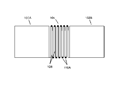
100081 Figure 1 depicts an overhead view of an embodiment of the present
invention
showing two device islands connected edge-to-edge by a monolithically formed
extremely
stretchable interconnect, prior to being stretched.
[00091 Figure 2 depicts an overhead view of an embodiment of the present
invention
showing two device islands connected edge-to-edge by two extremely stretchable
interconnects.
[00101 Figure 3 depicts an overhead view of an embodiment of the present
invention
showing two device islands connected edge-to-edge by three extremely
stretchable
interconnects; in this case, the long bars of the interconnects are rotated by
900 which allows
them to be longer than if they were not rotated.
[0011] Figure 4 depicts four device islands arranged in a square matrix in
an embodiment of
the present invention, with each edge connected by an extremely stretchable
interconnect to its
nearest neighbors island edge, and the interconnects are formed so as to
maximize the amount of
chip area that is used for either an island or interconnect.
[0012] Figure 5 depicts the case of Figure 1, with the short bars widened
for extra
mechanical strength at those locations.
[0013] Figure 6 depicts embodiments of the present invention, where (a) is
a side view of
device islands and extremely stretchable interconnects transferred onto an
elastomeric substrate.
In this case, the substrate has been molded to have posts that are of the same
area as the device
islands (note that in embodiments these could be smaller or larger than the
device islands). The
height "h" of the molded post regions may range from, but is not limited to,
about 1-1000 um.
3
CA 2780747 2019-11-28
CA 02780747 2012-05-11
WO 2010/056857 PCT/US2009/064199
The interconnects are located in between these regions as shown. (b) Side view
as before, with a
similarly shaped elastomeric superstrate to serve as an encapsulation layer
protecting the devices
from direct mechanical contact.
[0014] Figure 7 depicts a side view of a two-layer PDMS substrate in an
embodiment of the
present invention comprising silicon device islands adhered to top layer, free-
standing
interconnects, and square wave ripples in the lower layer PDMS to promote
increased stretching
through the substrate.
[0015] Figure 8 depicts an embodiment of the present invention with a side
view of two
layers of cured photoresist (SU-8 50 and SU-8 2002) used to make the two-layer
PDMS
substrate described in Figure 7.
[0016] Figure 9 depicts an embodiment of the present invention with a side
view of a two-
layer PDMS substrate consisting of sinusoidal waves in the lower layer of PDMS
to promote
increased stretching through the substrate.
[0017] While the invention has been described in connection with certain
preferred
embodiments, other embodiments would be understood by one of ordinary skill in
the art and
are encompassed herein.
[0018] All documents referenced herein are hereby incorporated by
reference.
DETAILED DESCRIPTION OF THE INVENTION
[0019] The present invention accomplishes extremely stretchable electronics
by forming the
electronics on discrete islands 102 of silicon.
[0020] With reference to the present invention, the term "stretchable", and
roots and
derivations thereof, when used to modify circuitry or components thereof is
meant to encompass
circuitry that comprises components having soft or elastic properties capable
of being made
longer or wider without tearing or breaking, and it is also meant to encompass
circuitry having
components (whether or not the components themselves are individually
stretchable as stated
4
CA 02780747 2012-05-11
WO 2010/056857 PCT/US2009/064199
above) that are configured in such a way so as to accommodate and remain
functional when
applied to a stretchable, inflatable, or otherwise expandable surface. The
term "expandable",
and roots and derivations thereof, when used to modify circuitry or components
thereof is also
meant to have the meaning ascribed above. Thus, "stretch" and "expand", and
all derivations
thereof, may be used interchangeably when referring to the present invention.
100211 In embodiments, the discrete islands mention above are discrete
operative (in
embodiments, arranged in a "device island" arrangement) and are themselves
capable of
performing the functionality described herein, or portions thereof. In
embodiments, such
functionality of the operative devices can include integrated circuits,
physical sensors (e.g.
temperature, pH, light, radiation etc), biological and/or chemical sensors,
amplifiers, AID and
D/A converters, optical collectors, electro-mechanical transducers, piezo-
electric actuators, light
emitting electronics which include LEDs, and combinations thereof. The purpose
and advantage
of using standard ICs (in embodiments, CMOS, on single crystal silicon) is to
have and use high
quality, high performance, and high functioning circuit components that are
also already
commonly mass-produced with well known processes, and which provide a range of
functionality and generation of data far superior to that produced by a
passive means.
[0022] In an example, the discrete islands 102 may range from about, but
not limited to, 10-
100 gm in size measured on an edge or by diameter, and connecting said islands
102A-B with
one or more extremely stretchable interconnects 104. The novel geometry of the
interconnects
104 is what makes them extremely compliant. Each interconnect 104 is patterned
and etched so
that its structural form has width and thickness dimensions that may be of
comparable size (such
as their ratio or inverse ratio not exceeding about a factor of 10); and may
be preferably equal in
size. In embodiments, the dimensions may not be greater than about 5um (e.g.
where both
dimensions are about 1 um or less). The interconnect 104 may be formed in a
boustrophedonic
style such that it effectively comprises long bars 108 and short bars 110 as
shown in Figure 1.
This unique geometry minimizes the stresses that are produced in the
interconnect 104 when
CA 02780747 2012-05-11
WO 2010/056857 PCT/US2009/064199
subsequently stretched because it has the effective form of a wire, and
behaves very differently
than interconnect form factors having one dimension greatly exceeding the
other two (for
example plates). Plate type structures primarily relieve stress only about a
single axis via
buckling, and withstand only a slight amount of shear stress before cracking.
This invention may
relieve stress about all three axes, including shears and any other stress.
100231 In addition, because the interconnect 104 may be formed out of rigid
materials, after
being stretched it may have a restorative force which helps prevent its wire-
like form from
getting tangled or knotted when re-compressing to the unstretched state.
Another advantage of
the boustrophedonic geometry is that it minimizes the initial separation
distance between the
islands 102A-B. This is illustrated in Figure 1. One or more interconnects 104
may be formed in
various ways, as shown in Figures 2-4. The parts of the interconnect 104 where
the majority of
stresses build up during stretching may be the short linking bars To minimize
cracking here, the
short linking bars 110A may be made several micrometers wider than the longer
bars 108, as
shown in Figure 5.
[0024] In embodiments, the connection point of the interconnect 104 to the
device island
102 may be anywhere along the device island edge, or may be at a point on the
surface of the
device island 102 (in which case the interconnect may be located just above
the plane of the
device island).
[0025] In embodiments, device islands 102 may be made on any suitable
material substrate,
provided that a top membrane layer of said substrate that contains the ICs can
be freed from the
bulk of the substrate and transfer printed onto an elastomeric substrate.
[0026] In the present invention, the interconnects 104 (as described
herein) may be formed
either monolithically (i.e., out of the same semiconductor material as the
device islands) or may
be formed out of another material. In one non-limiting example embodiment, the
stretchable
electronics are fabricated on a silicon-on-insulator (S01) wafer, having a 1
ium thick top silicon
layer and a lium thick buried oxide layer. Devices are formed on the top
silicon wafer, and
6
CA 02780747 2012-05-11
WO 2010/056857 PCT/US2009/064199
arranged into a square pattern of islands 102A-D and interconnects 104 of the
general form
shown in Figure 4, in which the islands 102 are 100 gm on an edge, and the
interconnects 104
are 1 gm wide, and the space between each long bar is 1 gm, and the
interconnects 104
comprise 10 long bars 108, all about 100 gm long. The islands 102 and
interconnects 104 are
formed in an etching step which removes the excess silicon. The islands 102
and interconnects
104 are coated with a 1 um layer of polyimide that is patterned to only cover
the islands 102 and
interconnects 104. Next, the islands 102 and interconnects 104 are released in
an HF etch which
undercuts the underlying buried oxide. After drying, the islands 102 and
interconnects 104 are
transfer printed with a Polydimethylsiloxane (PDMS) stamp onto an elastomeric
substrate 602.
After being picked up by the transfer stamp, and prior to being placed onto
the elastomeric
substrate 602, the backsides of the islands 102 may be coated with a layer of
polyimide
(patterned to only cover the islands 102 and interconnects 104), and an
additional layer of
evaporated 3 nm chromium and 30 nm silicon dioxide selectively over the island
regions to
improve adhesion to the elastomeric substrate 602 at those locations, and not
along the
interconnects 102. The elastomeric substrate 602 may be PDMS or another highly
compliant
material. The elastomeric substrate 602 may additionally be molded or etched
into the shape
shown in Figure 6A-B, to further increase selective adhesion in the device
island region but not
the interconnect region, and to reduce the amount of material strain in the
elastomeric substrate
602 that is transferred to the device islands 102. In this example, the
interconnects may
accommodate stretching the device islands apart by approximately up to 800 gm.
In addition,
the interconnects 104 of this example may be capable of accommodating lateral
shear
displacements of about 800 gm. In general, they may be capable of
accommodating any relative
displacement of the two islands such that they remain approximately within 800
gm of each
other. In addition, the interconnects 104 may accommodate corkscrew type
rotations of one
island relative to another about any of the three axes of rotation. This
feature may be limited
only by the interconnects becoming entangled within each other. In any
practical application, the
7
CA 02780747 2012-05-11
WO 2010/056857 PCT/US2009/064199
completed stretchable device may not be so severely rotated, and the
interconnect may easily
accommodate rotations of up to 1800. It is noted that by increasing the number
of long bars 108
used in the interconnect 104, or by increasing the length of the long bars
108, the interconnect
may be able to accommodate even larger displacement strains. In embodiments,
there may be
no practical upper limit to the amount of displacement enabled through the
present invention.
100271 In another embodiment the elastomeric substrate 602 may comprise two
layers
separated by a height. The top "contact" layer contacts the device island 102
as in the
embodiment illustrated in Figure 6. In addition, figure 7 shows the bottom
layer 702 may be a
"wavy" layer containing ripples or square waves molded into the substrate 602
during elastomer
fabrication. These square waves enable additional stretching, whose extent
depends on the
amplitude and wavelength of the waves pattern-molded in the elastomer 602.
Figure 7 shows
one non-limiting layout and topology of an elastomeric substrate 602 relative
to the position of
the interconnects 104 and device islands 102A-B. In an example, a two layer
molded substrate
can be fabricated using two step process consisting of two types of negative
photoresist (SU-8
50 and SU-8 2002; Microchem Corporation). The negative resists can be spin-
coated on a
transfer silicon wafer with spin speeds of 3000 rpm. The SU-8 50 layer can be
spun on the
wafer, and subsequently cured with UV radiation. Once the SU-8 50 layer has
hardened, the SU-
8 2002 can be spun and cured with a photo-mask and an alignment tool. In this
example, the
thickness of the SU-8 50 and SU-8 2002 are 40-50 gm 708 and 2-10 gm 704,
respectively. The
40-50 gm thick regions of SU-8 50 contain ripples 702 of SU-8 2002 (in this
instance in the
form of square waves) on their surfaces. Upon curing of the SU-8 2002 layer,
liquid PDMS can
be poured over the SU-8 patterns to form a substrate in the shape of the SU-8
molds 802, as
shown in Figure 8. The amplitude of the ripples in the SU-8 mold 802 can be
varied by changing
the spin speed used for spinning the thin layer of SU-8 2002. In this
configuration, the
interconnects 104 are free-standing. The entire substrate-device configuration
can be immersed
8
CA 02780747 2012-05-11
WO 2010/056857 PCT/US2009/064199
in non-cured elastomer (fluid layer) layer followed by a cured layer of PDMS
to encapsulate the
fluid and devices.
[0028] In another embodiment, the PDMS in the lower layer may be designed
with periodic
sinusoidal ripples 702B. In embodiments, this ripple configuration may be
achieved by bonding
Si nanoribbons on the surface of pre-strained PDMS in a uniform parallel
pattern. The release of
the prestrain in the PDMS substrate generates sinusoidal waves along the thin
Si-nanoribbons
(caused by buckling) and the surface of the PDMS substrate. The amplitude and
wavelength of
these waves 702B may depend on the extent of uniaxial pre-strain exerted on
the PDMS and on
the mechanical properties of the Si-nanoribbons. The wavy surface on the PDMS
may be used
as a transfer mold. Two-part liquid plastic solution can be poured over the
wavy PDMS
substrate and cured at room temperature over time (-2 hrs). Once the plastic
hardens, the plastic
substrate can be peeled away from the PDMS. This new plastic transfer
substrate with wavy
surface features can be used to produce more PDMS substrates containing wave
features. The
wavy PDMS may serve as the lower layer of PDMS as in the previous embodiment.
To produce
a two layer PDMS structure, a top layer of PDMS can be plasma bonded to this
lower layer of
PDMS using oxygen plasma surface activation to produce the substrate
illustrated in Figure 9.
[0029] In another embodiment, the PDMS transfer stamp is stretched after
the islands 102A-
B and interconnects 104 are picked up. A subsequent transfer to another
elastomeric substrate
602 may place these pre-stretched devices in a configuration, which allows the
new elastomeric
substrate to undergo compression. The devices may be able to accommodate that
compression
because the interconnects are pre-stretched.
[0030] In another embodiment, the interconnects 104 are not made out of the
same material
as the device islands 102. In this case, the islands 102A-B are completely
isolated from each
other by etching, with no interconnects in between. In an example, a layer of
polyimide may
then be deposited, contact vias etched to various locations on the surface of
the device island
102, and then metal interconnects 104 deposited and patterned into a
boustrophedonic pattern,
9
CA 02780747 2012-05-11
WO 2010/056857 PCT/US2009/064199
followed by another layer of polyimide. Both layers of polyimide may now be
patterned and
etched to leave a small border around the interconnects 104 (thereby fully
encapsulating the
interconnects). These interconnects may have the advantage that they are
already fully
encapsulated in polyimide and will not adhere as well to the elastomeric
substrate as the device
islands will. The other advantage is that these interconnects may not be
limited to only
connecting along the edge of an island. The contact via may be etched anywhere
on the surface
of the island 102, including near the center. This may allow for easier
connections to devices,
more connections than possible only along an edge, increased strain
compliance, decreased
strain at the contact vias, and multiple layers of interconnects made with
polymer passivation
layers in between, allowing even more interconnects, or allowing one device
island 102A to
connect to a non-neighboring device island 102B.
[0031] In another embodiment of the invention, the device islands 102 are
fabricated and
transfer printed onto the elastomeric substrate 602, or substrate comprising a
polymeric release
layer and polymeric non-release layer. After transfer printing, the
interconnects 104 are formed
as described above, which may be possible because they do not require any high
temperature
processing, and then in the latter case, the release layer is etched and the
devices that are on the
non-release layer, are transfer printed onto another elastomeric substrate
602. In the former case,
the islands 102 may be transferred onto the elastomeric substrate using pick
and place
technology so that islands 102 that are initially fabricated very close to
each other are spread
apart when they are transfer printed. This allows the interconnects 104 to be
fabricated in a
pattern that resembles their stretched configuration (if desired), to allow
compression.
[0032] In embodiments, the present invention may comprise a stretchable
electrical
interconnect 104, including an electrical interconnect 104 for connecting two
electrical contacts
102A-B (e.g. device islands 102A-B), where the electrical interconnect 104 may
be arranged
boustrophedonicially to define rungs 108 (i.e. long bars 108) between the
contacts 102A-B, and
where the rungs 108 may be substantially parallel with one another and where a
plurality of
CA 02780747 2012-05-11
WO 2010/056857 PCT/US2009/064199
rungs 108 may have substantially the same length and displacement
therebetween. In addition,
the ratio of the length of the plurality of rungs 108 and the displacement
between the plurality of
rungs 108 may be large, such as at least 10:1, 100:1, 1000:1, and the like.
The electrical
integrity of the electrical interconnect 104 may be maintained as stretched,
such as to
displacements that are increased to 1000%, 10000%, 100000%, and the like
during stretching.
In embodiments, the rungs 108 may be substantially perpendicular to the
contacts 102A-B, the
interconnection 104 may have a trace width and/or inter-rung spacing ranging
between 0.1-10
microns. In embodiments, the two electrical contacts 102A-B may be located on
an elastomeric
substrate 602, the electrical contacts 102A-B may be bonded to the substrate
602 and the
interconnection 104 not bonded to the substrate 602, the electrical contacts
102A-B may be
semiconductor circuits, metal contacts, and the like.
[0033] In embodiments, the present invention may comprise a stretchable
electrical
interconnect 104, including an electrical interconnect 104 for connecting two
electrical contacts
102A-B, where the electrical interconnect 104 is arranged boustrophedonicially
to define rungs
108 between the contacts 102A-B, and where the interconnect 104 maintains
electrical
conductivity and electrical integrity when a displacement between the contacts
102A-B is
increased, such as by 1000%, 10000%, 100000%, and the like.
[0034] In embodiments, the present invention may electrically interconnect
two electrical
contacts 102A-B with a stretchable interconnection 104 that has the ability to
twist between the
two electrical contacts 102A-B by up to approximately 180 degrees while
maintaining electrical
integrity of the stretchable interconnection 104.
[0035] In embodiments, the present invention may be a device including a
body having a
stretchable surface (e.g. an elastomeric substrate 602), and a stretchable
electronic circuit
including (i) a first discrete operative device 102A, (ii) a second discrete
operative device 102B,
and (iii) a stretchable interconnect 104 connecting the first discrete
operative device 102A to the
second discrete operative device102B, where the interconnect 104 may have a
substantially
11
CA 02780747 2012-05-11
WO 2010/056857
PCT/US2009/064199
boustrophedonic pattern and be able to maintain electrical conductivity when
stretched, such as
up to 1000%, 10000%, 100000%, and the like. The stretchable electronic circuit
may be
affixed to the stretchable surface of the body. In embodiments, the connection
may be to a metal
contact, to a semiconductor device, and the like. The first discrete operative
device 102A, the
second discrete operative device 102B, and the stretchable interconnect 104
may all be made
from the same material, and that material may be a semiconductor material.
[0036] In
embodiments, the present invention may attach at least two isolated electronic
components (which in embodiments may be discrete operative devices) 102A-B to
an
elastomeric substrate 602, and arrange an electrical interconnection 104
between the
components 102A-B in a boustrophedonic pattern interconnecting the two
isolated electronic
components 102A-B with the electrical interconnection 104. The elastomeric
substrate 602 may
then be stretched such that components 102A-B separate relative to one
another, where the
electrical interconnection 104 maintains substantially identical electrical
performance
characteristics that the electrical interconnection 104 had in a pre-stretched
form. In
embodiments, the stretching may be a translational stretching, where the
separation between the
isolated electronic components 102A-B increases by a percent as a result of
the stretching, such
as 10%, 100%, 1000%, 10000%, 100000%, and the like. The stretching may be a
rotational
stretching, where the rotation may be greater than a certain rotation angle,
such as 90 , 180 ,
270 , 360 , and the like, where the stretching may be in all three axes. In
embodiments, the
electrical interconnection 104 may be made from semiconducitve material. The
electrical
interconnection 104 may be made from the same semiconductor material as the
isolated
electronic components 102A-B, fabricated at the same time as the isolated
electronic
components 102A-B, and the like. The semiconductor material may be a single
crystal
semiconductor material. The electrical interconnection 104 may made of a
different material
than the isolated electronic components 102A-B, such as a metal. In
embodiments, the
interconnect material 104 may be loosely bound to the elastomeric substrate
602, not connected
12
CA 02780747 2016-07-07
at all, raised above the surface of the elastomeric substrate 602, and the
like. In embodiments,
the at least two isolated semiconductor circuits may be fabricated on an upper
surface 604 of the
elastomeric substrate 602 separated by a lower surface 608 of the elastomeric
substrate 602, and
the electrical interconnection 104 may be fabricated at the level of the upper
surface 604 of the
elastomeric substrate 602. In this way, the electrical interconnection 104 may
have no direct
contact with the lower level 608, and thereby be substantially free from
adhesion to the lower
level 608 during stretching. In addition, the lower surface 608 of the
elastomeric substrate 602
may include a wavy form 702, where the wavy form 704 may allow the elastomeric
substrate
602 to expand during stretching.
[0037] While the invention has been described in connection with certain
preferred
embodiments, other embodiments would be understood by one of ordinary skill in
the art and
are encompassed herein.
13