Note : Les descriptions sont présentées dans la langue officielle dans laquelle elles ont été soumises.
CA 02781043 2012-05-15
WO 2011/060353 PCT/US2010/056694
LATTICE-MISMATCHED CORE-SHELL QUANTUM DOTS
FIELD
The disclosure relates to lattice-mismatched core-shell quantum dots (QDs). In
certain
embodiments, the lattice-mismatched core-shell QDs are used in methods for
photovoltaic or
photoconduction applications. They are also useful for multicolor molecular,
cellular, and in
vivo imaging.
BACKGROUND
Nanometer scale particles made up of metals typically found in semiconductor
materials are generally referred to as quantum dots (QDs). Quantum dots of the
same
material, but of different sizes, can emit light of different colors. Surface
modification of
QDs with organic polymers allows one to tailor their properties and
incorporate the particles
into larger materials. QDs are currently used in numerous electronic and
biological
applications.
Quantum dots that display properties of Type-II band semiconductor materials
are
described in Kim et al., J. Am. Chem. Soc 125, 11466 -11467 (2003). See also
U.S. Patent
No. 7,390,568. Type-II QDs are expected to have useful properties because of
the spatial
separations of electron charge carriers. Type-II structures can allow access
to wavelengths
that would otherwise not be available with a single material. In addition, the
separation of
charges in the lowest excited states of type-II nanocrystals makes these
materials more
suitable in photovoltaic or photoconduction applications. Thus, there is a
need to identify
improved Type-II QDs.
SUMMARY
The disclosure relates to lattice-mismatched core-shell quantum dots (QDs). In
certain
embodiments, the disclosure relates to lattice-mismatched QDs formed by
epitaxial deposition
of a compressive shell, e.g., ZnS, ZnSe, ZnTe, CdS or CdSe, onto a soft core,
e.g., CdTe or
the core has a bulk modulus of less than about 52, 51, 50, 54, 53, 52, 51, 50,
49, 48, 47, 46,
45, 44, or 43 GPa.
1
CA 02781043 2012-05-15
WO 2011/060353 PCT/US2010/056694
In certain embodiments, the lattice-mismatched quantum dots comprise a core
and a
compressive shell wherein the lattice mismatches are greater than about 7.5,
8.0, 8.5, 9.0, 9.5,
10.0, 10.5, 11.0, or 11.5%. In certain embodiments, the core has a lattice
constant greater
than about 0.5, 0.6, 0.7, 0.8, or 0.9 angstroms than the epitaxial deposited
compressive shell.
In certain embodiments, core material is CdTe and a lattice constant for the
compressive shell
is less than about 6.0, 5.9, 5.8, 5.7, or 5.6 angstroms.
In certain embodiments, the disclosure relates to lattice-mismatched core-
shell
quantum dots comprising a XTe core coated with a compressive shell wherein X
is Cd or Hg
wherein the core and shell is not CdTe/CdSe. Typically, the core is CdTe and
the compressive
shell comprises ZnS, ZnSe and/or CdS. In certain embodiments, the core
diameter is about
1.8, 2.0, 2.2, 2.5, 2.8, 3.0, 3.5, or 4.0 nm or the core diameter is less than
about 2.0, 2.5, 3.0,
3.5, 4.0 4.5, or 5.0 nm. In certain embodiments, the compressive shell has two
or more
monolayers of ZnS, ZnSe, ZnTe, CdS or CdSe or one or more monolayers of ZnO,
ZnS,
ZnSe, ZnTe, CdO, CdS, CdSe, CdTe, MgO, MgS, MgSe, MgTe, HgO, HgS, HgSe, HgTe,
AN, AlP, AlAs, AlSb, GaN, GaP, GaAs, GaSh, InN, InP, InAs, InSb, T1N, T1P,
T1As, T1Sb,
T1Sb, Pbs, PbSe, PbTe, or mixtures thereof. In certain embodiments, the
thickness of the
compressive shell is more than 1.8, 2.0, 2.2, 2.5, 2.8, 3.0, 3.5, 4.0, 5.0,
6.0, 7.0, 8.0, 9.0, or
10.0 nm.
In certain embodiments, the QDs have a polymer over the compressive shell with
carboxylic acid groups, monomers with thiol groups, and monomers with amino
groups. In
certain embodiments, the polymer does not contain polyethylene glycol
monomers. In certain
embodiments, the quantum dots disclosed herein are contained in a polymer or
glass matrix.
In certain embodiments, the QDs have a biological material conjugated to the
compressive shell such as a nucleic acid, polypeptide, cell, antibody,
epitope, protein,
inhibitor, receptor, or receptor substrate. In certain embodiments, the
lattice-mismatched
core-shell QDs are used in methods for multicolor molecular, cellular, and in
vivo imaging.
In certain embodiments, the disclosure relates to photovoltaic cells and
devices
comprising quantum dots provided herein. In certain embodiments, the
disclosure relates to
light-emitting diode comprising quantum dots as provided herein. In certain
embodiments,
the disclosure relates to a laser comprising QDs disclosed herein.
2
CA 02781043 2012-05-15
WO 2011/060353 PCT/US2010/056694
BRIEF DESCRIPTION OF THE FIGURES
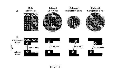
Figure 1 illustrates band energy changes in quantum dots induced by lattice
strain. a,
Lattice strain of ordinary and strained (CdTe)ZnSe nanocrystals. b, Valence
and conduction
band energy levels for the corresponding structures in a. The wavy arrows and
their colors
indicate band-edge fluorescence emission and their approximate wavelengths.
The horizontal
band lengths correspond to the thicknesses of the core and the shell. Relaxed
nanostructures
form standard type-I heterojunctions but are converted to type-II behavior
when the core is
`squeezed' and the shell is `stretched' by the strain from heteroepitaxial
growth. The impact
of strain is calculated using the model-solid theory and a continuum
elasticity model.
Figure 2 shows data on optical properties of strain-tuned QDs. a,b, Absorption
(left)
and fluorescence (right) spectra of (CdTe)ZnSe QDs with 1.8-nm (a) and 6.2-nm
(b) CdTe
cores, capped with different thicknesses of ZnSe. c, Strain-tunable spectral
ranges for
different CdTe core sizes, as measured by the fluorescence emission peaks with
0 - 5 ML of
shell growth. d, Time-resolved fluorescence decay curves of 3.8-nm CdTe cores
capped with
ZnSe shells of different thicknesses. The excited state lifetimes were
calculated to be 18.4
(core), 35.5 (1.5 ML), 59.8 (3.0 ML) and 115.0 ns (6.0 ML).
Figure 3 illustrates comparison of emission wavelengths and quantum yields for
different (core)shell and multilayered structures. a, Emission wavelengths of
3.8-nm CdTe
cores capped with CdSe (purple), ZnSe (red) or ZnTe (green), or one monolayer
of CdSe
followed by ZnSe (CdSe/ZnSe; black), or one monolayer of ZnTe followed by ZnSe
(ZnTe/ZnSe; blue). b, Quantum yields of a 3.8-nm CdTe core capped with 1-5 ML
CdSe
(purple) or ZnSe (red), or a 3.8-nm CdSe core capped with 1 - 5 ML ZnS
(brown). c, Bulk
band structures for the materials in a. d, Quantum-confined and strained band
structures
calculated using model-solid theory and a continuum elasticity model.
Figure 4 shows powder X-ray diffraction (XRD) and transmission electron
microscopy (TEM) data of strain-tunable QDs. a, XRD patterns for 3.8-nm CdTe
and
(CdTe)ZnSe QDs with 2, 6 or 9 ML of shell. Bulk diffraction peaks for zinc
blende (ZB)
ZnSe (top) and ZB CdTe (bottom) are indexed. b, TEM of 3.8-nm CdTe QDs (top
left) and
(CdTe)ZnSe QDs with 2 (top right), 6 (bottom left) or 9 (bottom right) ML of
shell. c,
HRTEMs with fast-Fourier transforms of 3.8-nm CdTe QDs (top) and (CdTe)ZnSe
QDs with
3
CA 02781043 2012-05-15
WO 2011/060353 PCT/US2010/056694
6 ML of shell (bottom). d, HRTEM of (CdTe)ZnSe QDs with 6 ML shell. Scale
bars: b, 20
nm; c, 5 nm; d, 5 nm.
Figure 5 shows continuum elasticity simulation data for high-strain (CdTe)ZnSe
QDs.
a, Left: strain distribution in a 3.8-nm CdTe nanocrystal coated with a 6 ML
ZnSe shell,
modeled as concentric spheres (solid black line) or concentric cylinders
(dashed red line).
Strain in the core is isotropically compressive, but strain in the shell is
tangentially tensile (top
line) and radially compressive (bottom line). Right: calculated lattice
constants corresponding
to spherical and cylindrical strain profiles, compared to the experimental
lattice constants
(blue dashed line). b, Coherent versus incoherent crystal growth as a function
of core size and
shell thickness.
Figure 6 shows data comparing optical tunability and fluorescence quantum
yields for
CdTe cores coated with different shell materials and thicknesses. (A) Emission
wavelengths
of 3.8 nm CdTe cores capped with ZnSe, CdS, or ZnS as a function of shell
thickness. (B)
Fluorescence quantum yields of the same QDs plotted as a function of shell
thickness.
Figure 7 illustrates the preparation of a polymer ligand coating over typical
QDs
disclosed herein. Typically one first exchanges the native ligands with
thioglycerol. These
polar monovalent ligands are then replaced with the multidentate ligand.
Stable, compactly
coated QDs are produced after heating (60-70 C) for 1-2 hours in DMSO under
inert
conditions.
DETAILED DESCRIPTION
Strain manifests itself uniquely in colloids because the epitaxial layer and
its substrate
can strain each other synergistically (i.e., interactive straining) and alter
their respective
properties. Experimental and theoretical calculations reveal that much higher
strain can be
tolerated in small nanocrystals than their bulk counterparts. Small
nanocrystals (less than 5
nm) have a high surface area to volume ratio and highly curved surfaces,
allowing the stress
from a lattice-mismatched epitaxial shell to be distributed over a large
fraction of the
constituent atoms. For larger nanocrystals and bulk substrates, the total
number of atoms is
larger, and the epitaxial stress is imposed on a surface that contains a
smaller fraction of the
4
CA 02781043 2012-05-15
WO 2011/060353 PCT/US2010/056694
constituent atoms, favoring the formation of strain-relaxing crystalline
defects rather than
homogeneous strain.
Heteroepitaxial strain within coreshell QDs can be used to alter the optical
properties
of these nanocrystals. In particular, epitaxial growth of a compressive shell
material (ZnS,
ZnSe, ZnTe, CdS or CdSe) on a small and soft nanocrystalline core (CdTe)
dramatically
changes the conduction energy band. The lattice strain can control the
locations of charge
carriers, modulate the excited state lifetimes, tune the absorption and
emission spectra across
a broad wavelength range, and minimize the spectral overlap between absorption
and
emission. These results are different from the small spectral shifts (5 - 7
nm) observed by
Chen et al., for CdSe QDs, which are likely not caused by lattice strain but
arise from the
continuous growth of CdSe cores (not CdS shells) under their experimental
conditions. Chen
et al., Nano Lett. 3, 799 - 803 (2003). Strain-tunable QDs have uses in solar
energy
conversion, multicolor biomedical imaging, and super-resolution optical
microscopy based on
stimulated emission depletion.
Lattice strain in colloidal nanocrystals
Lattice strain can induce significant bandgap energy changes when a shell
material is
coherently grown on a small and compressible nanocrystalline core. See Fig. 1.
In the bulk
state, hetero-structures of CdTe and ZnSe have valence and conduction bands
that are aligned
to localize both the electrons and holes in CdTe (type-I behavior). On the
nanometer scale,
however, epitaxial growth of a ZnSe shell strongly compresses a CdTe
nanocrystal because
the lattice parameter of ZnSe (5.668 A) is considerably smaller than that of
CdTe (6.482
A). For zinc blende II - VI and III - V semiconductors, the electronic energy
gap
increases with applied compressive force, and decreases under tensile strain.
The conduction
band shifts to a larger degree than the valence band and therefore the
compressive
deformation of CdTe induced by shell growth increases the energy of the
conduction band. At
the same time, the shell material is under tensile strain, resulting in a
decrease in its
conduction band energy. These two strain effects work in a concerted fashion
(that is, double
straining) to alter the energy band offsets, converting standard type-I QDs
into type-II
heterostructures, resulting in a spatial separation of the electrons and
holes. As the shell grows
in thickness, the core conduction band energy rises due to increased
compressive strain from
5
CA 02781043 2012-05-15
WO 2011/060353 PCT/US2010/056694
the shell, while the shell's conduction band energy decreases due to a
reduction in quantum
confinement.
Properties of strain-tuned nanocrystals
With increasing epitaxial shell growth of ZnSe on CdTe, the optical absorption
and
fluorescence emission spectra are dramatically shifted towards longer
wavelengths (lower
energies) (Fig. 2a). Small spectral changes are also observed in type-I QDs
when a finite
potential well of the shell allows tunneling of the electron and hole between
the core and the
shell. In the case of (CdTe)ZnSe, however, additional shell growth continues
to shift the
absorption band-edge and the emission maximum, beyond the band-edge energy of
bulk CdTe
(1.50 eV) and ZnSe (2.82 eV) (see Fig. 2a). Several lines of evidence suggest
that this redshift
is due to a transformation to type-II band alignment: (i) a gradual reduction
of distinct optical
absorption features; (ii) a decrease in the band-edge oscillator strength, and
(iii) a significant
increase in excited state lifetimes (Fig. 2d). These changes are caused by
spatial separation of
holes into the core and electrons into the shell, resulting in a decrease in
the electron - hole
overlap integral. Colloidal type-II quantum dots such as (CdTe)CdSe can
achieve charge
carrier separation through the selection of specific materials with staggered
band offsets for
the core and shell. See Kim et al., J. Am. Chem. Soc. 125, 11466 - 11467
(2003). Type-II
band alignments allow spatially indirect recombination at energies lower than
the bulk
bandgap energies of either of the individual semiconductors.
The largest spectral shifts are observed with very small cores, such as 1.8-nm
CdTe,
allowing tuning from the green to the near- infrared spectra. In contrast,
larger CdTe cores
cannot be effectively compressed through epitaxy, and their emission spectra
are much less
tunable by lattice strain. The strain-tunable spectral ranges are shown in
Fig. 2c for differently
sized CdTe cores. It is remarkable that QDs with small cores can be tuned to
emit beyond the
spectral ranges of large dots, at both the blue and red sides of the emission
spectra. This novel
phenomenon has not been observed for other types of quantum dots. Depending on
the core
size and shell thickness, these QDs can be tuned to emit between 500 and 1,050
nm with a
quantum efficiency between 25 and 60%. The fluorescence peak width is
consistently
between 40 and 90 nm (full-width at half-maximum, FWHM) in the near infrared
(700 - 900
nm), a `clear window' well suited for biomedical imaging applications.
6
CA 02781043 2012-05-15
WO 2011/060353 PCT/US2010/056694
An interesting finding is that the strain-induced spectral changes are gradual
and do
not exhibit an abrupt transformation as might be expected for a switch from
type-I to type-II.
For core sizes less than 4 nm in diameter, our data indicate that the
transition to type-II
behavior is `complete' after capping with 2 - 3 monolayers (ML) of shell
material, as defined
by the complete disappearance of the first exciton absorption peak. Between 0
and 2 - 3 ML,
however, the behavior of these QDs lies between type-I and type-II. Here, one
of the charge
carriers is strongly confined to one region of the nano- crystal (in our case,
the hole is
confined to the core), whereas the other charge carrier (the electron) is
weakly confined, being
largely delocalized across the entire nanocrystal.
Strain in multilayered structures
To further understand the separation of electrons and holes in these strained
nanostructures, systematic capping experiments were carried out in which
interim shell layers
are used to provide specific energy barriers to either the hole or the
electron (Fig. 3). Capping
CdTe with a CdSe shell is known to generate type-II QDs with the electron
located in the
shell, due to the lower conduction band energy level of CdSe compared to CdTe.
In contrast,
capping CdTe with a ZnTe shell or an interim layer of ZnTe provides a large
barrier to
electron diffusion out of the QD core, but little impediment to hole diffusion
out of the core.
Capping CdTe with CdSe yields a type-II QD with a substantial decrease of the
bandgap,
whereas ZnTe capping only slightly changes the band gap. By using one
monolayer of these
materials as a barrier to hole or electron diffusion, overgrowth of ZnSe leads
to a type-II
structure only when grown with the CdSe interim layer. Little redshift is
observed for QDs
with an interim layer of ZnTe, confirming that electron diffusion into the
shell is important for
the strain-induced type-II structure to function. Hole confinement to the core
is also
supported by the high quantum efficiency of these (core)shell QDs, as surface
hole traps are
more detrimental to the optical properties of QDs than are electron traps.
It is remarkable that the highly strained (CdTe)ZnSe heterostructures (14.4%
lattice
mismatch) are able to maintain excellent photoluminescence properties. The
high quantum
yield may be attributable to the high crystallinity of the initial CdTe cores
(quantum yield up
to 80%), and the homogeneity of shell growth at high temperatures (shell
growth was
incomplete and non-uniform below 200 Q. Also, the lattice compressibility is
considerably
7
CA 02781043 2012-05-15
WO 2011/060353 PCT/US2010/056694
higher for CdTe (bulk modulus Bu = 42.4 GPa) and ZnSe (Bu = 62.4 GPa)
(considered to be
softer because of their lower modulus values) than the commonly used QD
materials CdSe
(Bu = 53.1 GPa) and ZnS (Bu = 77.1 GPa). Thus, the ability of CdTe and ZnSe to
elastically
compress when subjected to a large stress, rather than relaxing to form defect
trap sites,
allows these QDs to maintain their excellent spectral properties. These QDs
maintain a high
quantum yield after 2 ML of shell growth (Fig. 3b), unlike similarly strained
(CdSe)ZnS QDs
(12% lattice mismatch), which reach a peak in quantum yield after roughly 1.5
ML of shell
growth. This difference is likely due to the inability of the less elastic
CdSe and ZnS to
withstand strain without forming defects. Using the softer CdTe core, growing
both CdS and
ZnS shells (11.4% and 19.8% lattice mismatches, respectively) produces QDs in
which a high
quantum yield is maintained even after 3 ML of shell growth.
The concept of strain-induced defect formation has been the predominant
paradigm for
understanding the photoluminescence efficiency of (core)shell QDs, but this
concept does not
account for the low quantum efficiencies of type-II QDs. Xie et al., reported
that type-II
(ZnTe)CdSe QDs have a quantum yield of 15 - 20%, which decreases after growth
of
1.5ML, despite a lattice mismatch of only 0.6%. Adv. Mater. 17, 2741 - 2745
(2005).
Figure 3b shows data suggesting that type-II (CdTe)CdSe QDs (7.1 % lattice
mismatch) reach
a peak in fluorescence efficiency after only 1ML of shell growth, whereas
highly strained
(CdTe)ZnS QDs (19.8% lattice mismatch) reach a peak fluorescence efficiency
after 2.5
- 3 ML of shell growth (see Fig. 6). Thus, (CdTe)ZnS and (CdTe)ZnSe QDs are
more
desirable than (CdTe)CdSe QDs if they have a sufficiently thick shell to red
or infrared-shift
the fluorescence and maintain adequate quantum yields resulting in light
emission with high
quantum yields (60%) across a broad spectrum of visible and near-infrared
wavelengths (500
to 1,050 nm).
The separation of charge carriers in type-II QDs can result in a decreased
probability
of radiative recombination, and the extended excited-state lifetimes may
increase the
probability of nonradiative recombination events. In addition, one of the
charge carriers in
type-II QDs is confined to the shell region, and this carrier thus has an
increased probability
of being trapped in a surface defect site, a major factor governing the
photoluminescence
efficiency of QDs.
8
CA 02781043 2012-05-15
WO 2011/060353 PCT/US2010/056694
Structural characterization
Powder X-ray diffraction (XRD) data (Fig. 4a) shows that certain QDs grow
homogeneously as uniform crystalline domains. The CdTe cores show a zinc-
blende crystal
structure, which shifts to smaller bond lengths with shell growth. After 6 ML
(monolayers) of
shell growth, the lattice constant has shrunk by 5.1 % relative to zinc blende
CdTe, indicating
an expansion of the ZnSe shell lattice by 8.5% compared to bulk. Further
increasing the shell
thickness to 9 ML nearly doubles the total nanocrystal volume, but only
slightly changes the
lattice parameters. The diffraction peaks become narrower due to the larger
crystalline
domains produced, with no evidence of pure ZnSe or CdTe domains. Combined with
the
quasi-spherical morphology of these particles observed in transmission
electron microscopy
(TEM) images (Fig. 4b), these data suggest that crystal growth is coherent and
homogeneous,
despite the large strain between the core and the shell materials. The XRD
spectra show
patterns of a hexagonal lattice with shell growth, indicated by splitting of
the (111) reflection
and the development of a peak between the (220) and (311) reflections.
However, simulations
of the diffraction patterns of these structures reveal that these observations
are not indicative
of a phase change. Instead, these changes reflect the polymorphic nature of II
- VI materials,
which are commonly found to be poly- types of wurtzite (hexagonal) and zinc
blende (cubic)
phases in bulk and as nanostructures. This polytypism manifests itself in
stacking faults in the
[I I I] zinc blende direction, which can be prevalent even in highly
crystalline materials due to
the minute energy difference between these two structures. Our structural
simulation data
demonstrate that all of the (core)shell nanocrystals characterized in Fig. 4
are pre- dominantly
zinc blende, with 30 - 40% of the (111) lattice planes stacked in the
hexagonal
geometry. Therefore, the increasing hexagonal nature of the diffraction
patterns is caused
solely by the narrowing of the diffraction peaks with coherent shell growth,
which reveals the
underlying cubic - hexagonal polytypism that is obscured by the wide
diffraction peaks of
small cores.
High-resolution TEM data (Fig. 4c,d) further reveal the coherent crystallinity
of these
QDs, with lattice planes extending throughout the entire nanocrystal. Lattice
warping and
electron-density differences were also observed for strained core - shell
structures.
However, other than low-energy stacking faults, no major crystalline defects
are observed,
consistent with the high quantum yield and band-edge emission observed
throughout shell
9
CA 02781043 2012-05-15
WO 2011/060353 PCT/US2010/056694
growth. Nearly all QDs with shells larger than 2 ML were identified to be
oriented with the
zinc blende (111) plane parallel to the TEM grid. This anisotropy is in
agreement with XRD
patterns and simulations of samples with thick shells (Fig. 4a), showing
narrower and more
intense peaks for the nanocrystal reflections perpendicular to the [111] axis.
This preferential
growth is attributed to the anisotropy of the underlying zinc blende CdTe
cores, which are
found to be slightly elongated in the [I I I] direction (Fig. 4c). The
prevalence of wurtzite
stacking faults in this direction adds a fundamental degree of anisotropy in
the underlying
crystalline lattice. Importantly, the lattice mismatch between the wurtzite
structures of the
core and shell materials is slightly larger in the a-direction compared to the
c-direction, and
the compressibility of wurtzite II - VI materials is higher in directions
perpendicular to the c-
axis. This suggests that shell growth may be favored to propagate in the
radial direction,
outward along the cylindrically shaped QDs. This mode of shell growth
contrasts with that
observed for most CdSe nanocrystals, which typically favor growth in the c-
direction of
wurtzite structures, commonly attributed to the high reactivity of the c-
terminal facet and
closer lattice match in this direction.
CdTe is the most compressible of all the II - VI and III - V materials except
for
mercury telluride, and its deformation potential is also high. This means that
the lattice of
CdTe is readily compressed, and upon compression, its electronic energy bands
shift to a
large degree. ZnSe also has a high deformation potential but has a much higher
bulk modulus;
its role as a less deformable, highly mismatched shell material is likely
important in
generating the unique optical properties reported. In comparison, core-shell
QDs with better
lattice matching (such as (CdTe)CdS and (CdSe)CdS) exhibit considerably less
spectral
shifting due to the reduced lattice strain and lower deformation potential
values. Furthermore,
nearly all (core)shell nanocrystals and other types of nano-heterostructures
are subject to
varying degrees of lattice strain due to structural mismatches.
Continuum elasticity modeling
To gain further insight into the mechanism of strain tuning, a continuum
elasticity
model for coherently grown epitaxial ZnSe shells on spherical CdTe cores was
implemented
(Fig. 5). With radial compression from the shell, the core is found to be
under isotropic,
compressive strain. The shell lattice is under tensile strain in the tan-
gential directions
CA 02781043 2012-05-15
WO 2011/060353 PCT/US2010/056694
surrounding the core, and compressively strained in the radial direction. The
strain in the shell
decays with increasing distance from the interface, but does not decay fully
to zero. This
result demonstrates that thick shells are unable to compress the core to more
than a critical
value, leaving a significant amount of elastic strain in the shell. Based on
the lattice constants
experimentally observed from XRD and TEM, the compression of the core should
be much
larger. This discrepancy is most likely due to the nonspherical growth in the
shell occurring
perpendicular to the [111] direction causing the heterostructure to more
closely resemble
concentric cylinders rather than concentric spheres. As shown in Fig. 5a,
modeling this
system as cylinders redistributes much of the strain to the shell, and more
strongly correlates
with the experimentally observed lattice parameters. Using this theoretically
derived lattice
deformation, we have used the model-solid theory to calculate the band offsets
and bandgaps
of the various (core)shell structures. The bandgaps of these structures at
various stages of
shell epitaxial growth were predicted. In addition, the continuum elasticity
model can be used
to predict the shell thickness for which the formation of a dislocation loop
is energetically
more favorable than coherent, epitaxial growth. Figure 5b depicts this
thickness for different
core sizes, demonstrating that CdTe QDs with a diameter less than about 3.5 nm
can tolerate
strained, coherent growth of ZnSe shells of essentially any thickness.
For these modeling calculations, bulk material parameters are used because no
general
trends have emerged regarding the dependence of material properties on
particle size.
Compressibility typically changes with grain size, most commonly showing a
softening effect
with decreasing size. In other instances, their compressibility values are
found to be
unchanged in nanoparticles compared to the bulk. For II - VI semiconductors,
it has been
reported that CdS QDs have similar compressibilities compared to the bulk,
whereas CdSe
QDs are more compressible than the bulk material. Quantum confinement by
itself may
induce structural modifications in semiconductor nanocrystals, and these
nanocrystals may be
subject to compressive or tensile forces depending on the nature of their
passivating ligands.
For the strain-tunable QDs disclosed herein, the elasticities of nanoscale
ZnSe and CdTe have
not been determined as a function of particle size. If the elasticities of the
core and shell
materials decreased evenly, the total elastic strain energy in these dots
would be reduced. This
energy reduction is not expected to alter crystalline deformation or lead to
major net changes
in our bandgap calculations. To further examine the case in which only one of
the materials
11
CA 02781043 2012-05-15
WO 2011/060353 PCT/US2010/056694
becomes more elastic, a theoretical model was implemented using smaller
elastic moduli (for
example, 20% smaller than bulk) for either the core or shell materials. This
softening effect
marginally modifies the magnitude of the strain-induced band shifting (by less
than 3%). The
observed crystalline polytypism may slightly affect the calculated bandgaps.
Wei and
colleagues calculated a bandgap 1.50 eV for zinc blende CdTe and a bandgap of
1.547 eV for
wurtzite. For ZnSe, experimental data of the bandgaps also reveal a very small
difference of
2.82 eV for zinc blende and 2.85 eV for wurtzite.
Electronic devices
In certain embodiments, the disclosure relates to electronic devices
comprising
quantum dots disclosed herein. In certain embodiments, visual displays utilize
light emitting
diodes that contain quantum dots disclosed herein. Materials comprising the
quantum dots
are position between an anode and a cathode. Charge-carriers-electrons and
holes-flow
into the junction from electrodes with different voltages. When an electron
meets a hole, it
falls into a lower energy level, and releases energy in the form of a photon.
In certain embodiments, the disclosure relates to a film comprising quantum
dots that
is placed adjacent to a light emitting diode. The light emitting diode
produces light that is
absorbed by the quantum dot causing the quantum dot to emit light, e.g.,
fluoresce.
In certain embodiments, a system comprises a transparent film comprising
quantum
dots, and light emission layer, between a hole-transporter layer (HTL) and an
electron-
transport layer (ETL).
Organic electroluminescent materials are typically in favor of injection and
transport
of holes rather than electrons. Thus, the electron-hole recombination
generally occurs near the
cathode. In order to prevent the produced excitons or holes from approaching
cathode, a hole-
blocking layer plays dual roles in blocking holes moving towards the cathode
and transporting
the electrons to the emitting QD layer. Tris-Aluminium (A1g3), bathocuproine
(BCP), and
TAZ are typically used hole-blocking materials.
In certain embodiments, a device comprises a metal cathode, e.g., Au and Ag, a
electron transporting layer (ETL), e.g., ZnO:SnO2 (ratio 1:3), a light
emission layer
comprising the quantum dots disclosed herein, energy barrier layer, e.g.,Si02,
and a hole
12
CA 02781043 2012-05-15
WO 2011/060353 PCT/US2010/056694
transporting layer (HTL), e.g., p-silicon. Resistivity of p-type silicon may
be about 10-100
ohm cm. The emission may be observed through the top metal cathode.
The array of quantum dots may be manufactured by self-assembly in process
known
as spin-casting; a solution of quantum dots in an organic material is poured
into a substrate,
which is then set spinning to spread the solution evenly.
Contact printing process for forming QD thin film is generally described in
Kim et al.,
(2008) Nano Letters 8: 4513-4517. The overall process of contact printing
typically
comprises providing a polydimethylsiloxane (PDMS) molded stamp; coating the
top side the
PDMS stamp with a thing film of parylene-c, a chemical-vapor deposited (CVD)
aromatic
organic polymer; inking the parylene-c coated stamp is via spin-casting of a
solution of
colloidal QDs suspended in an organic solvent; and contact printing the formed
QD
monolayer transformed on to the substrate after the solvent evaporates.
In certain embodiment, the disclosure relates to devices comprising an
electrode such
as indium tin oxide coated with p-paraphenylene vinylene and a film comprising
quantum
dots disclosed herein. The quantum dots may be held together with multidentate
ligands such
as an alkyl dithio, hexane dithiol and held to the surface of the electrode.
See Colvin et al.,
Nature 1994, 370, 354, hereby incorporated by reference.
In certain embodiments, the disclosure relates to light emitting diodes
comprising
films of conjugated polymers such as poly[2-methoxy-5 -(2-ethylhexyloxy)- 1,4-
phenylenevinylene] (MEH-PPV) and or poly[(9,9-dihexylfluorenyl-2,7-diyl)-co-
(1,4-{benzo-
[2,1',3]thiadiazole})] (F6BT) and quantum dots disclosed herein. See Tessler
et al., Science
2002, 295, 1506, hereby incorporated by reference.
In certain embodiments, the disclosure relates to light emitting diodes
comprising
quantum dots disclosed herein coated with a layer of trioctylphosphine oxide
(TOPO) and/or
trioctylphosphine (TOP). The coated quantum dots can be arranged between
electrodes, e.g.,
indium tin oxide (ITO) coated on a glass substrate, and adjacent to a hole-
transporting
material such as a N,N'-diphenyl-N,N'-bis(3-methylphenyl)-(1,1'-biphenyl)-4,4'-
diamine
(TPD) layer. See Coe et al., Nature 2002, 420, 800, hereby incorporated by
reference.
Opposite the TPD layer the quantum dot layer may be adjacent to a film of tris-
(8-
hydroxyquinoline)aluminium (A1g3) in contact with a cathode or optionally a
layer of 3-(4-
biphenylyl)-4-phenyl-5 -t-butylphenyl- 1,2,4-triazole (TAZ) introduced between
the A1g3
13
CA 02781043 2012-05-15
WO 2011/060353 PCT/US2010/056694
layer. In other embodiments, the quantum dots are in a layer on top of a layer
of a conducting
polymer such as poly (3,4-ethylenedioxy thiophene):polystyrenesulfonate. See
Hikmet et al.,
J. Appl. Phys. 2003, 93, 3509, hereby incorporated by reference.
Solar energy conversion
In certain embodiments, the disclosure relates to quantum dot solar cells,
e.g., solar
cells with a coating of nanocrystals. A thin film of nanocrystals is obtained
by spin-coating.
Quantum dot based photovoltaic cells typically utilized dye-sensitised
colloidal Ti02 films.
In certain embodiments, the solar cell comprises a pair of electrodes wherein
a layer of
quantum dots disclosed herein is between the electrodes, typically contained
in a polymer
film, e.g., poly (3-hexylthiophene). One electrode may be an indium tin oxide
substrate
optionally coated with poly(ethylene dioxythiophene) doped with polystyrene
sulfonic acid
(PEDOT:PSS, a conducting polymer). See Huynh et al., Nature 2002, 295, 2425,
hereby
incorporated by reference.
In certain embodiments, the solar cell comprises Ti02 film adjacent to quantum
dots
disclosed herein and a hole transport layer of the conjugated polymer poly(9,9-
dioctyl-
fluorene-co-N-(4-butylenphenyl)diphenylamine). The cells are typically
prepared on
fluorinated tin oxide (FTO) coated glass following a layer-by-layer growth
using aqueous
solutions of the polycations, poly(ethyleneimine) (PEI), poly (diallyl
dimethylammonium
chloride) (PDDA), negatively charged Ti02 nanoparticles in basic solution, and
negatively
charged quantum dots disclosed herein. See Kniprath et al., Thin Solid Films.
518 (1), 295-
298 (2009), hereby incorporated by reference.
Biological applications
Quantum dots can be used in any biological applications where traditional
organic
dyes are utilized. QDs are typically superior to traditional organic dyes
because of brightness
(owing to the high extinction co-efficient combined with a comparable quantum
yield to
fluorescent dyes) and stability (allowing much less photobleaching).
The photostability of quantum dots allows the acquisition of many consecutive
focal-
plane images that can be reconstructed into a high-resolution three-
dimensional image.
Another application of quantum dot probes is the real-time tracking of
molecules and cells
14
CA 02781043 2012-05-15
WO 2011/060353 PCT/US2010/056694
over extended periods of time. Antibodies, streptavidin, peptides, nucleic
acid aptamers, or
small-molecule ligands can be used to target quantum dots to specific proteins
on cells.
In certain embodiments, the disclosure relates to the use of quantum dots
disclosed
herein for in vitro imaging of pre-labeled cells, e.g., imaging single-cell
migration in real time
for embryonic cells, cancer cells, stem cells, and lymphocytes. For example,
quantum dots
disclosed herein may be use for tumor targeting under in vivo conditions by
active targeting
and passive targeting. In the case of active targeting, quantum dots are
functionalized with
tumor-specific binding sites to selectively bind to tumor cells or the tumor
microenvironment.
Passive targeting utilizes the enhanced vascular permeability of blood vessels
in cancer tissue
for the delivery of quantum dot probes. Tumors typically have a more permeable
endothelium than normal tissue allowing the leakage of small nanoparticles
into the cancer
tissue interstitium. Moreover, tumor cells lack an effective lymphatic
drainage system, which
leads to subsequent nanoparticle-accumulation.
The surface of quantum dots disclosed herein may be tailored to interact with
the
biological sample through electrostatic and hydrogen-bonding interactions or
through specific
ligand-receptor interactions such as avidin-biotin interactions. In certain
embodiments, the
quantum dots disclosed herein are coated with a layer of silica, e.g., coating
them with 3-
(trihydroxylsilyl) propyl methylphosphonate, in order to make them water
soluble or
methoxysilylpropyl urea and acetate for bind to cellular nuclei. In other
embodiments, biotin
is covalently bound to the surface of the quantum dots. See Bruchez et al.,
Science 1998, 281,
2013 hereby incorporated by reference.
Conjugating biological material to quantum dots can be accomplished by a
variety of
methods. The biological materials may recognize a specific analyte such as a
protein, nucleic
acid, or virus. Mercaptoacetic acid may be use as a ligand for solubilization
and covalent
protein attachment. When reacted with ZnS-capped QDs, the mercapto group binds
to a Zn
atom, and the polar carboxylic acid group renders the QDs water-soluble. The
free carboxyl
group is available for covalent coupling to various biomolecules (such as
proteins, peptides,
and nucleic acids) by cross-linking to reactive amine groups. See Chan & Nie,
Science 1998,
281, 2016, hereby incorporated by reference.
In certain embodiments, the quantum dots disclosed herein are coated with
biological
molecules by utilizing electrostatic attractions between negatively charged
lipoic acid and
CA 02781043 2012-05-15
WO 2011/060353 PCT/US2010/056694
biologically engineered bifunctional recombinant (chimeric) proteins
comprising positively
charged attachment domains (containing a leucine zipper) genetically fused
with desired
biologically relevant domains. See Mattoussi el al., J. Am. Chem. Soc. 2000,
122, 12142
hereby incorporated by reference.
In certain embodiments, the disclosure relates to quantum dots disclosed
herein coated
with ligands. In certain embodiment, the ligands are multidentate polymers.
Polymer ligands
minimize the hydrodynamic size of QDs, provided colloidal stability and
prevent
photobleaching. In certain embodiments, the disclosure relates to polymer
ligands that
contain a mixed composition of thiol (-SH) and amine (-NH2) groups grafted to
a linear
polymer. See Smith & Nie, J Am Chem Soc. (2008) 130(34): 11278-11279, hereby
incorporated by reference. Representative amphiphilic polymers are disclosed
in Smith et al.
Phys. Chem. Chem. Phys 2006;8:3895-3903; Pons et al., J. Phys. Chem. B
2006;110:20308-
20316, and Pellegrino et al., Nano Lett 2004;4:703-303, all hereby
incorporated by
reference.
In certain embodiments, the ligands are conjugated to a biological molecule or
targeting molecule which can be a nucleic acid, polypeptide, cell, antibody,
epitope, protein,
inhibitor, receptor, or receptor substrate. The nucleic acid molecule may be a
probe that
hybridizes to a known polymorphic sequence that provides a specific genotype.
The
polypeptide may target a desired cell marker, i.e., receptor of a protein that
is displayed on the
surface of a cell that indicates the cell type. They may be dendritic cell
markers, endothelial
cell markers, B cell markers, T cell markers, natural killer cell markers,
cancer cell markers,
plasma cell markers, or hemapoietic cell markers.
Quantum dots disclosed herein may be cross-linked to biomolecules such
antibodies,
oligonucleotides, or small molecule ligands to render them specific to
biological targets. See
Smith et al., Adv. Drug Deliv. Rev. 60, 1226 - 1240 (2008), hereby
incorporated by
reference. This may be accomplished using standard bioconjugation protocols,
such as the
coupling of maleimide-activated QDs to the thiols of reduced antibodies. The
surfaces of
QDs may be modified with bio-inert, hydrophilic molecules such as polyethylene
glycol, to
eliminate possible nonspecific binding, or to decrease the rate of clearance
from the
bloodstream following intravenous injection. QDs disclosed herein may emit
fluorescence
without an external source of excitation when conjugated to enzymes that
catalyze
16
CA 02781043 2012-05-15
WO 2011/060353 PCT/US2010/056694
bioluminescent reactions, due to bioluminescence resonance energy transfer
(BRET). See So
et al., Nat. Biotechnol. 24 (2006), pp. 339-343, hereby incorporated by
reference.
In certain embodiments, quantum dots disclosed herein are cross-linked to
small
molecule ligands, inhibitors, peptides, or aptamers can bind with high
specificity to many
different cellular receptors and targets. See Lidke et al., Nat. Biotechnol.
22 (2004), pp. 198-
203, hereby incorporated by reference.
In certain embodiments, the quantum dots disclosed herein can be use in
sensors for
detection of specific nucleic acid sequences. By mixing a single stranded
nucleic acid to be
detected with (a) an acceptor fluorophores conjugated to a nucleic acid
fragment
complementary to one end of the target and (b) a biotinylated nucleic acid
fragment
complementary to the opposite end of the target nucleic acid, these
nucleotides hybridize to
yield a biotin-nucleic acid-fluorophore conjugate. Upon mixing this conjugate
with quantum
dots disclosed herein fluorescence is quenched via nonradiative energy
transfer to the
fluorophore conjugate. This dye acceptor then becomes fluorescent,
specifically and
quantitatively indicating the presence of the target nucleic acid. See Zhang
et al., Nat. Mater.
4 (2005), pp. 826-831, hereby incorporated by reference.
Terms
The "bulk modulus" refers to a material's resistance to uniform compression,
i.e., the
pressure increase needed to cause a given relative decrease in volume with a
base unit is the
pascal. In the case of a nanoparticle core it refers to the bulk modulus of
the core material as
determined in larger dimensions e.g., millimeter dimensions. One can measure
the bulk
modulus using powder diffraction under applied pressure or by other methods
known in the
art. See, e.g., Al-Douri et al., Physica B: Condensed Matter, 322, (1-2),
2002, 179-182.
A "lattice constant" or "lattice parameter" refers to the constant distance
between unit
cells in a crystal lattice. Lattices in three dimensions generally have three
lattice constants,
referred to as a, b, and c. In the case of cubic crystal structures, all of
the constants are equal.
Similarly, in hexagonal crystal structures, the a and b constants are equal.
Unless otherwise
proved the "lattice constant" refers to the average lattice constant in three
dimensions. Lattice
constants are typically on the order of several angstroms (i.e. tenths of a
nanometer). Lattice
17
CA 02781043 2012-05-15
WO 2011/060353 PCT/US2010/056694
constants or mismatches can be determined using techniques such as X-ray
diffraction or with
an atomic force microscope. Some lattice constants are provided in the table
below.
Element or Crystal Lattice Constant
Compound Type Name Structure at 300 K (A)
C Element Carbon (Diamond) DIAMOND 3.56683
Ge Element Germanium Diamond 5.64613
Si Element Silicon Diamond 5.43095
Sn Element Grey Tin Diamond 6.48920
SiC IV-IV Silicon carbide Wurtzite a=3.086;
c= 15.117
AlAs III-V Aluminum arsenide Zincblende 5.6605
AlP III-V Aluminum phosphide Zincblende 5.4510
AlSb III-V Aluminum antimonide Zincblende 6.1355
BN III-V Boron nitride Zincblende 3.6150
BP III-V Boron phosphide Zincblende 4.5380
GaAs III-V Gallium arsenide Zincblende 5.6533
GaN III-V Gallium nitride Wurtzite a=3.189;
c=5.185
GaP III-V Gallium phosphide Zincblende 5.4512
GaSb III-V Gallium antimonide Zincblende 6.0959
InAs III-V Indium arsenide Zincblende 6.0584
InP III-V Indium phosphide Zincblende 5.8686
InSb III-V Indium antimonide Zincblende 6.4794
CdS II-VI Cadmium sulfide Zincblende 5.8320
CdS II-VI Cadmium sulfide Wurtzite a=4.160;
c=6.756
CdSe II-VI Cadmium selenide Zincblende 6.050
CdTe II-VI Cadmium telluride Zincblende 6.482
ZnO II-VI Zinc oxide Rock Salt 4.580
ZnS II-VI Zinc sulfide Zincblende 5.420
ZnS II-VI Zinc sulfide Wurtzite a=3.82; c=6.26
PbS IV-VI Lead sulfide Rock Salt 5.9362
PbTe IV-VI Lead telluride Rock Salt 6.4620
18
CA 02781043 2012-05-15
WO 2011/060353 PCT/US2010/056694
EXPERIMENTAL
Example 1: Synthesis of CdTe cores.
(Core)shell QDs were prepared by using a two-step organometallic approach in a
high-temperature coordinating solvent. CdTe cores of various sizes (1.8 - 6.2
nm) were
synthesized by swiftly injecting a room-temperature solution of
trioctylphosphine (TOP)-
telluride (0.1 mmol in 5 ml octadecene) into a hot (300 C) solution of cadmium
oxide (0.2
mmol), tetradecylphosphonic acid (0.44 mmol), hexadecylamine (5.7 mmol) and
octadecene
(10 ml total). The growth temperature was set to 265 C and the final size of
the CdTe QD core
was controlled by varying the growth time, and by slow injection of additional
precursors if
larger sizes were desired. After cooling to room temperature, the luminescent
nanoparticles
(quantum efficiency 40-80%) were diluted in hexane, centrifuged to remove the
insoluble
cadmium precursor, purified by means of repeated hexane - methanol
extractions, and finally
centrifuged again to remove potential nanocrystal aggregates.
Example 2: Shell growth.
A modified version of the successive ion layer adsorption and reaction (SILAR)
procedure, originally described by Peng et al., was used J. Am. Chem. Soc.
119, 7019 - 7029
(1997). Specifically, at the initial capping temperature (TML1), a solution
was injected
containing a cation precursor (0.1 M diethylzinc or dimethylcadmium dissolved
in TOP),
containing the amount of precursor required to constitute a 0.25 ML shell.
After 10 min,
which was experimentally determined to be a sufficient amount of time to
prevent
homogeneous nucleation of the shell material, the anion precursor was injected
(0.1 M
sulphur, selenium or tellurium, dissolved in TOP). After this second
injection, shell growth
was allowed to proceed for a period of time dependent on the initial growth
temperature and
the shell composition. For example, for the growth of ZnSe on CdTe, the
following reaction
times were used: 4 h for 150 8C, 2 h for 170 8C and 30 min for 210 - 225 8C.
For other shell
materials, however, it was found that the shell growth rate was strongly
dependent on the
reactivity of the precursors. Both diethylzinc and dimethylcadmium were highly
reactive at all
of the temperatures used in this work. These reactions were limited by the
deposition rate of
the chalcogen. Generally, tellurium and selenium reacted efficiently at low
temperatures (for
example, 2 h reaction time at 170 C), but initial growth of CdS and ZnS
required extended
19
CA 02781043 2012-05-15
WO 2011/060353 PCT/US2010/056694
times, up to 8 h before completion on 1.8-nm cores at 140 C. After the first
two injections at
TML1, a second pair of injections was performed to grow 1 ML of total shell on
the cores,
using the same reaction time for the first 0.5 ML.
Once this thin layer of shell material was deposited on the QDs, indicated by
spectral
redshifting, the temperature threshold of these QDs towards ripening was
significantly
enhanced. This is due to a combination of the increase in overall size of the
nanocrystals, the
greater bond strength and thermal stability of the shell materials used in
this study (CdS,
CdSe, ZnSe, ZnS and ZnTe) compared to the cores (CdTe), as well as the greater
strength of
bonding of the amine and phosphine ligands to the shell material, compared to
CdTe. After
the deposition of just 1 ML, the temperature of the reaction could therefore
be increased
drastically without optical signs of ripening. In this manner, the growth
temperature was
increased to a point at which the reaction was much more efficient, and
shorter reaction times
could be used to complete shell growth. The deposition of ZnSe on CdTe was
optimized for
all of the sizes tested, but the deposition of the other shell materials (ZnS,
ZnTe, CdS and
CdSe) was optimized for 3.8-nm QD cores. For this procedure, 0.25 ML
increments were
used so that the surface stoichiometry of anions and cations would be similar
for each 0.5 ML
shell growth cycle. When performed with 0.5 ML increments, like the SILAR
procedure
originally described by Peng et al., there was a significant decrease in
quantum yield after
each anion injection, thus obscuring the relative changes in fluorescence
quantum yield,
which is in accord with previous findings. The important experimental
parameters for the
synthesis of strain-tunable QDs are summarized in the Table 1, and shell
thickness data is
provided in Table 2.
Table 1
CdTe core [QC] TO\rf TMML9 TÃ1L TML34 TML-5-e T L7-3
Size p q }ry
1.8 nn 28 pM 15000 14011C 1900C 225CC 25D'C n.Ca.
3.8 nm 6.0 l.N 170' C 1.500C 225 C 2250C 250 C 2.6000
5.2 nm 4.0 p M 210"C 190 C 225 C 220' C 250 C n.a.
6.2 nm 3.0 pM 230 C 22511C 225 `C 225"C 2501:'C n.a.
CA 02781043 2012-05-15
WO 2011/060353 PCT/US2010/056694
Table 2
Shell d;_ (nm) dT-LS (nrm) d-r C (nrn) di j (11M)
thickness (r) relaxed strained relaxed strained
6 (core) n.a. 3.75 n. a. n.a. n.a. n a.
2 ML 595 4.66 4.74 5.04 4.22 4.60
6 ML 3671 7.37 6.85 7.31 7.08 7.79
9 ML 6446 10.51 8.50 9.20 9.71 10.91
Example 3: Nanocrystal characterization.
Steady-state fluorescence spectra were obtained using a spectrofluorometer
(Photon
Technology International). A xenon lamp was used for excitation, a
photomultiplier tube was
used as a detector for the spectral range 400 - 800 nm, and an InGaAs detector
for the range
800 - 1,700 nm. The spectrometer slit widths were typically operated at 4 nm.
Quantum yield
measurements were performed by comparison to Atto dyes (520, 565, 610 or 680)
dissolved
in ethanol, accounting for differences in solvent refractive index. Absorption
spectra were
measured on a Shimadzu spectrophotometer with 1-nm slit widths. Time-resolved
fluorescence decay spectra were obtained with excitation from a 478-nm pulsed
diode laser. A
spectrometer was used to resolve the peak emission wavelength, detected using
a
photomultiplier tube. TEM images were obtained with a Hitachi H-7500 TEM, and
high-
resolution imaging was performed on a Hitachi H-9500. X-ray diffraction
spectra were
measured using a Bruker SMART 1000 CCD/Hi-Star dual-detector diffractometer,
with a
cobalt X-ray source.
Example 4: Simulation of X-ray diffraction spectra.
Methods to simulate the X-ray diffraction spectra of small nanocrystals using
the
Debye equation have been previously described in detail. See Bawendi, et al.,
J. Chem. Phys.
91, 7282-7290 (1989). Briefly, 20 zinc blende crystal lattice structures were
constructed with
randomly distributed wurtzite stacking faults in the [I I I] direction with a
specific frequency
(0 - 100%). Atoms were removed from these structures that fell outside a
specific nanocrystal
shape and size. Core CdTe QDs were simulated as about 850 atom hexagonal
cylinders, and
(core)shell structures were simulated by extending the lattices of these cores
using zinc and
selenium atoms. The Debye equation was then solved for these structures using
the DISCUS
21
CA 02781043 2012-05-15
WO 2011/060353 PCT/US2010/056694
software package. The spectra were averaged to simulate a distribution of
stacking faults.
Only ten spectra were averaged for the 6 and 9 ML samples due to the long
processing times
required for such large structures. Thermal effects were incorporated through
Debye-Waller
factors; however, it should be noted that strain would be expected to have an
effect on thermal
fluctuations of atoms, but in ways that are not immediately predictable. No
surface relaxations
were incorporated in the simulations. For comparison with experimental data,
the
backgrounds of experimental spectra were first conservatively subtracted.
Example 5: Polymer synthesis.
HO .,O
. IC
2. P. 410-f , Id 1 :1 it ' le
M.
F
Polyacrylic acid (PAA, MW 1773), N-hydroxysuccinimide (NHS), N,N'-
diisopropylcarbodiimide (DIC), cysteamine, (3-mercaptoethanol (BME), 1-
thioglycerol,
dimethylsulfoxide (DMSO), dimethylformamide (DMF), cadmium oxide, tellurium,
dioctylether (DOE), 5,5'-dithiobis(2-nitrobenzoic acid) (Ellman's reagent),
glycine, L-
cysteine, acetone, chloroform, methanol, hexane, and piperidine were purchased
from Sigma.
N-Fmocethylenediamine (Fmoc-EDA) was purchased from ABD Bioquest.
Tetradecylphosphonic acid (TDPA) was obtained from Alfa Aesar. Oleylamine was
from
Acros Organics, trioctylphosphine (TOP) was from Strem, and fluorescamine was
purchased
from Invitrogen.PAA (1 g, 13.9 mmol carboxylic acids) was mixed with 25 mL
DMSO in a
150 mL three-necked flask. After stirring for 24 hours at 35 C, freshly
prepared anhydrous
solutions of cysteamine (187 mg, 2.43 mmol) and Fmoc-EDA (686 mg, 2.43 mmol),
each
dissolved in 6 mL DMSO, were added. The solution was protected from light and
bubbled
with argon for 30 minutes at 35 C. After the addition of an anhydrous solution
of NHS (1.12
mg, 9.71 mmol) in 6 mL DMSO, DIC (736 mg, 5.83 mmol) was slowly added over the
course
of 40 minutes during vigorous stirring. Bubbling was continued for 30 minutes,
and then the
22
CA 02781043 2012-05-15
WO 2011/060353 PCT/US2010/056694
reaction was allowed to proceed for 7 days at 40 C in the dark. Piperidine (18
mL) was then
added, and the solution was stirred for four hours to deprotect the primary
amines. BME (501
mg, 6.41 mmol) was added to quench the reaction, and the solution was stirred
for 2 hours at
40 C, then cooled to room temperature and filtered. The mixture was condensed
to -4 mL at
45 C under vacuum (-40 Pa), and the polymer was precipitated with the addition
of a 2:1
mixture of ice-cold acetone: chloroform, and isolated via centrifugation. The
polymer was
dissolved in -5 mL anhydrous DMF, filtered, and precipitated again with
acetone-chloroform.
This process was repeated three times, and the polymer was finally washed with
acetone,
dried under vacuum, and stored under argon. This modified polymer was a white
powder,
soluble in water, DMSO, DMF, or methanol, but insoluble in acetone, unlike
PAA. If stored
under air, this polymer darkened and became yellow-brown over the course of a
few weeks,
and also became increasingly difficult to dissolve in various solvents.
Example 6: Synthesis of CdTe nanocrystals.
CdO (25.7 mg, 0.2 mmol), TDPA (122 mg, 0.44 mmol), and DOE (2 mL) were added
to a three-necked flask and heated to 250 C under argon until complete
dissolution of CdO.
After cooling to room temperature, oleylamine (1 g, 3.74 mmol) and 6.5 mL DOE
were
added. The solution was heated to reflux under vacuum (-20 Pa, -65 C) for 1
hour and then
heated to 300 C under argon flow. A second solution, containing tellurium
(12.76 mg, 0.1
mmol), TOP (2 mL), and DOE (3 mL), was injected into the cadmium precursor
solution, and
the growth temperature was set to 265 C. Using this method, highly
monodipserse
nanocrystals could be grown between 2.5 and 3.5 nm diameter after reaction
times between
20 seconds and 10 minutes. To grow larger nanocrystals, additional cadmium and
tellurium
precursors were sequentially injected dropwise into the reaction solution,
starting at 4 minutes
after the first injection. After reaching the desired size, the reaction
mixture was cooled to
room temperature, diluted with 85 mL hexane, and centrifuged to remove most of
the excess
cadmium precursor. The QDs were isolated using at least six hexane-methanol
extractions.
On the final extraction, the QDs were condensed to - 1 mL through the addition
of methanol.
These QDs were then diluted to -20 mL with chloroform, bubbled with argon for
30 minutes
and stored at 4 C in the dark. QD size was determined from its known
correlation with the
first exciton peak wavelength, and verified via TEM.
23
CA 02781043 2012-05-15
WO 2011/060353 PCT/US2010/056694
Example 7: Ligand exchange with 1-thioglycerol.
Purified CdTe QDs (2.5 nm) in chloroform (7 mL, -150 uM) were added to a three-
necked Ligand exchange with 1-thioglycerol flask connected to a Schlenk line.
Under intense
stirring, neat 1-thioglycerol was added dropwise until the first visible sign
of flocculation.
Then 4 mL of DMSO was added dropwise. An excess of 1-thioglycerol (3 mL) was
then
added, and chloroform was removed under vacuum at 25 C. After stirring for an
additional 2
hours at 25 C under argon, the QDs were precipitated with the addition of an
ice-cold mixture
of acetone: chloroform (1:1, 193 mL total). Following centrifugation, the
pellet was washed
with acetone and dried under vacuum.
Example 8: Coating quantum dots with the multidentate polymer ligand.
Two techniques were used to coat 1-thioglycerol QDs with the modified polymer,
as
depicted in Figure 7. In the first method, CdTe QDs coated with 1-thioglycerol
were
suspended in basic water (50 mM sodium hydroxide), centrifuged at 7000g for 10
minutes,
and then filtered to remove aggregated nanocrystals. Various amounts of
polymer dissolved in
basic water were added to the QDs, which were then gently mixed. Using this
method,
addition of an excess of ligand resulted in complete precipitation of the QD
over the course of
several hours. In the second method, QDs coated with 1-thioglycerol were
suspended in
DMSO and centrifuged at 7000g for 10 minutes to remove possible nanocrystal
aggregates.
The nanocrystals were diluted to -5-20 M for smaller sizes (2.5-3.5 nm), or -
2-5 M for
larger nanocrystals. The QDs were then degassed extensively at room
temperature and
charged with argon. An anhydrous DMSO solution of the polymer (-5 mg/mL) was
added
under vigorous stirring. The solution was then heated to 60 C for 90 minutes
for smaller QDs
(2.5-3.5 nm), or 70-75 C for 120 minutes for larger nanocrystals. In the
absence of the
polymer, the nanocrystals aggregated and precipitated from solution during
heating. Indeed,
the multidentate polymer greatly enhances the thermal stability of these
nanocrystals, as there
was no evidence of Ostwald ripening of 2.5 nm cores up to -130 C. After
cooling the QDs to
room temperature, ice-cold aqueous sodium hydroxide (50 mM, twice the volume
of DMSO)
was slowly added, and the solution was stirred for 2 hours. The QDs were then
extensively
24
CA 02781043 2012-05-15
WO 2011/060353 PCT/US2010/056694
dialyzed against basic water for 2-3 days using 25 kDa molecular weight cutoff
dialysis
tubing (Spectra/Por).