Note : Les descriptions sont présentées dans la langue officielle dans laquelle elles ont été soumises.
CA 02784801 2016-04-27
- 1 -
METHOD FOR PRODUCING A COMPONENT THAT CAN BE
ACTIVATED TO EMIT LIGHT
The invention relates to a process to manufacture a component that can be
activated to emit
light whereby the light emission is done by electroluminescence (EL).
First it should be explained that electroluminescence means the characteristic
of certain
materials or material combinations in which light is emitted in the visible
range in response to
an electrical alternating current. From practical applications,
electroluminescent films are
known in which the electroluminescent material is excited to light up by an
electrical
alternating field in a special condenser configuration. Such
electroluminescent films are often
also called luminescent films, light films, or condenser luminescent films. In
technical
applications they serve to convert electrical energy into light.
Furthermore, in practical applications there is the need for lighting or
backlighting components
with any surface/topography. Only by way of example, reference is made to
instrument panel
indicators in the front of a passenger car, operating knobs, pushbuttons and
other elements such
as information panels, etc.
The above-referenced electroluminescent films are excellent for use in
components which need
to be lit or backlit or made transparent provided these components have a
simple geometry. The
electroluminescent films are only of limited use in complicated structures,
particularly in three-
dimensional heavily structured surfaces. Only by way of example, reference is
made to IMD
CA 02784801 2012-06-18
- 2 -
technology (In Mould Decoration, cp. DE 197 17 740 C2), whereby films and,
e.g.,
electroluminescent films are injected to the backside of the carrier to
produce molds by injection
molding technology. Heavily structured surfaces, particularly miniaturized
components with
electroluminescent surfaces, however, cannot be produced by applying this
known process.
In particular, the lighting of classic speedometer needles thus far was done
by light-guiding
systems whereby it is necessary to couple the light into the turning or rather
oscillating/swiveling
speedometer needle: This is technically cost-intensive. Still, this technology
is mainly realized
thus far.
The purpose of the invention at hand is to specify a process to produce a
component that can be
activated to emit light by which the light is emitted through
electroluminescence (EL). The
process according to the invention shall allow covering nearly any structural
surfaces and
particularly very tiny or delicate components with electroluminescent layers,
which allows
lighting the surface of any functional elements, the interior of the material
or the rear of the
material/component.
According to the invention, initially a carrier is produced or provided,
whereby the carrier has
and includes essentially the form of the component and its mechanical and
electrical interfaces. In
this context, it is essential that the carrier is a type of blank for the
component to be produced,
namely a blank that does not yet possess the electroluminescent
characteristic. Mechanical
== CA 02784801 2012-06-18
-3 -
interfaces, e.g., in the form of an integral coupling element, can be an
integral part of the carrier.
Electrical interfaces can also be provided from the start or would be realized
on the surface at an
appropriate position during the production process.
In reference to the process according to the invention, it is of great
significance that the carrier
will be equipped with the functional layers of EL lighting, whereby at least
one of the functional
layers, namely the light-emitting layer or layers will be realized through the
tampon printing
process in whole or at least in part. The electrical interfaces¨also in the
area of the functional
layers¨are integrated into the print process so that the print technology
process of the light-
emitting layer/layers creates at the same time an electric contact. Subsequent
contacting, which
usually requires a significant constructive or process-technological time and
effort, is
unnecessary.
After the functional layers of the EL lighting are realized, a transparent or
translucent cover is
applied to the EL layers, which serves on the one hand as moisture protection
and on the other
hand as electrical and mechanical encapsulation. Therefore, with the
application of the final
cover, the component that can be activated to emit light, e.g., a speedometer
needle is completed.
As specified above, at least the light-emitting layer is realized by way of
tampon print. This is an
indirect printing process which works according to the so-called gravure
printing principle. The
pad takes on the color according to the outside contour of the cavity of the
printing plate and
CA 02784801 2012-06-18
=
- 4 -
reproduces it during imprinting on a component with any surface. These can be
restricted or
sequential areas and they can have various shapes¨also sequentially
restricted.
While it has been recognized that the tampon printing process, which thus far
has been normally
used to apply print on plastic objects mostly in the advertising material
industry, is particularly
suitable to realize a light-emitting layer within the scope of EL lighting; in
particular, because
this process imprints the color also on three-dimensional surfaces or into
deeper-lying areas. In
addition, during the use of the tampon printing process it is of great
importance that the color is
transferred to the respective carrier at nearly 100% because of the technology
underlying the
tampon printing process. This already allows reducing the production costs
significantly. It is also
conceivable to print several layers whereby the result is lighter and darker
light emissions.
The carrier may have nearly any topology on the surface. In general, the
material may be rigid or
flexible, e.g., in the form of an MID or metal-containing flexible plastics.
The electroluminescent
layer can be applied to structured surfaces using the tampon printing process,
whereby the carrier
can be equipped already beforehand with the electrical connections. Therefore,
contacting and
insulation between the various EL layers can be applied at the same time the
EL layer is applied,
whereby the insulating layers can be applied or generated in any way desired.
In addition to the
printing process, the contact surface can also be realized without any effort
with the injection
mold technology.
CA 02784801 2012-06-18
- 5 -
The electrical connections or the electrodes of the EL functional layers can
be generated in
various ways, e.g., by injection mold technology and/or print technology. In
this context, it is
conceivable to realize the electrical connections on and/or in the carrier. By
overprinting or
coating the connections, these can be coupled electrically or insulated
depending on the used
material. In addition, mask-like coatings or layers can be generated on the
electrical
connections/electrodes.
The light-emitting layer/layers is/are imprinted in the form of word and/or
picture information as
needed. The tampon printing process allows realization of structured surfaces
along the surface
profiles and strictly delineated areas with and without light-emitting layers.
The variety of
information which can be produced in this manner is limitless. In particular,
the light-emitting
layer may be formed on various levels, e.g., in a manner that any
interruptions and repeat
electrical connections are possible through direct imprinting of electrical
connections.
Everywhere where it is necessary, the insulating intermediate areas or
intermediate layers can
also be generated with printing or injection mold technology.
The functional layers are also imprinted by inserting insulators to generate
the full function of the
EL functional layers.
At this point, it should be mentioned that the process according to the
invention uses the tampon
printing process to generate at least the light-emitting layer/layers. In
general, it is conceivable
CA 02784801 2012-06-18
- 6 -
that additional functional layers, also light-emitting layers, can be
generated with the tampon
printing process as well as the injection mold process, lacquering technology,
etc. The same
applies to the insulators which are imperative for the construction of the EL
functional layers.
Furthermore it should be pointed out here that EL lighting, the use of EL
functional layers defines
any design of such functional layers to generate so-called EL lamps. It is not
considered
necessary to describe the precise design or the actual wiring because these
are well-known from
numerous reference works. Only as an example, additional reference should be
made to DE 102
34 125 Al, whereby the EL functional layers are provided in form of an EL
film.
The EL functional layers but at least the light-emitting layer encapsulating
cover can be produced
with the so-called 2K reaction process, whereby the CCM process (Clear Coat
Moldering) is
especially suitable. With this process, a sort of macro-encapsulating of the
EL functional layers is
possible, whereby the outer contour of the component can be covered or even a
shape can be
realized. The material used here can be transparent so that it can be lit
through an underneath EL
lamp generated by EL functional layers. In addition, it is conceivable to
color the material of the
cover or encapsulation. This allows generating a color filter in a perfect
manner.
It is also conceivable to cover the EL functional layers with a translucent
lacquer, whereby a so-
called laser lacquer can be used. A laser is used to literally burn the laser
lacquer so that any type
CA 02784801 2016-04-27
- 7 -
of light geometries, and therefore the overall contour of the lighted area on
the surface of the
component, can be created.
The enclosure¨however it can be generated¨can be applied to the outline and/or
reprocessed
in relation to the surface. Finally, it is even possible to process the outer
contour. This measure
or these measures are also suitable to generate any type of surface
structures, whereby in these
cases the EL functional layers may lay underneath.
Furthermore, it should be noted that the carrier can comprise or include any
number of
electronic components; in particular, in highly miniaturized form. In addition
it is conceivable
to assign the carrier its own power source/a source of voltage, e.g., by using
the solar voltaic
layers to create practically a self-sustaining component. In particular, it is
conceivable that any
number of functional elements are or will be included in the carrier, e.g.,
through vacuum
casting technology. There no limits in this case either.
According to one embodiment, there is provided a method to manufacture a
component that
can be activated to emit light whereby the light emission is done by
electroluminescence (EL),
the method comprising the following steps: providing and producing a carrier
in the form of the
component and its mechanical and electrical interfaces, wherein the carrier, a
connecting pin,
and an insulation collectively define contains a single electrical and
mechanical coupling
medium that connects the component both mechanically and electrically;
printing the carrier
with one or more functional layers of EL lighting, whereby: at least one of
the one or more
functional layers is generated with a tampon printing process; and the
electrical interfaces are
integrated into the print; and generating at least one of a transparent or
translucent cover as
protection from moisture and for electrical and mechanical encapsulation,
wherein the cover is
applied via a 2K reaction process such as a Clear Coat Molding (CCM) process.
In connection with the explanation of the preferred implementation examples of
the invention
based on the drawing, the generally preferred arrangements and advancements of
the teaching
are explained. The drawing illustrates in
CA 02784801 2012-06-18
- 8 -
Fig. 1 a schematic view of the basic design of an implementation example
of a
component with the EL functional layers necessary for light emission in
accordance with the invention, in
Fig. 2 a schematic view of the exemplary design of a component that
includes a so-called
EL lamp with mechanical and electrical interface, and in
Fig. 3 in a flowchart, schematically, possible process steps to produce a
component that
can be activated to emit light.
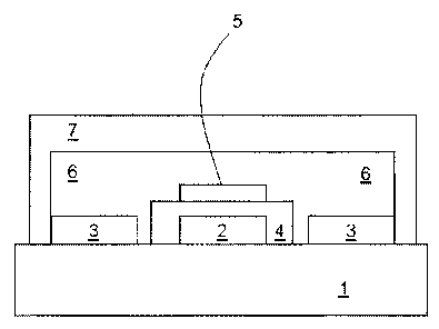
Fig. 1 shows an implementation example of a component produced according to
the invention
process, which includes an EL lamp to be activated to emit light.
The design shown in Fig. 1 demonstrates that the component includes initially
a carrier 1. This
can be any plastic substrate. The precise form is immaterial.
On carrier 1, a rear electrode 2 is applied. Furthermore, a ground wire 3 is
provided. These are
the electrical connections of the component.
The rear electrode 2 is covered by a dielectric 4. In addition, the dielectric
4 insulates the rear
electrode 2 from the ground wire 3.
An electroluminescent layer 5 is applied with the tampon printing method to
the dielectric 4. The
electroluminescent layer 5 is covered by a conductive lacquer 6 which is at
the same time the
CA 02784801 2012-06-18
=
- 9 -
electric contact for the ground wire 3. All functional layers of the EL
lighting can be imprinted.
Furthermore, the entire arrangement is covered by a sealing encapsulation 7,
which has the effect
of a macro-encapsulation namely for moisture protection and for electrical and
mechanical
encapsulation of the entire structure.
Fig. 2 shows in a schematic view another component, which is produced
according to the
invention, namely also with an integrated EL lamp.
The carrier 1 includes the electrical and mechanical coupling medium 8,
whereby contacting is
suggested by an AC voltage source 9. Between the carrier element 1 and an
electrically
conductive connection pin 10, an insulation 11 made of plastic is planned.
Therefore, it is
possible to connect the component shown in Fig. 2 both mechanically and
electrically, namely
due to the electrical/mechanical coupling medium 8 provided there.
The EL lamp of the component shown in Fig. 2 is similarly constructed as the
EL lamp of the
component shown in Fig. 1. The rear electrode 2 is formed by connecting pin
10. On top is the
dielectric 4, which covers connecting pin 10 together with insulation 11. The
EL layer 5 is
applied to dielectric 4, which in turn is covered by the conductive lacquer 6.
A color coat 12 is applied to the conductive lacquer 6 in the implementation
example selected in
Fig. 2. It serves as color filter in reference to the light emission from EL
layer 5.
CA 02784801 2012-06-18
- 10 -
The entire arrangement is CCM-overmolded, whereby the exterior shape of the
component is
more or less defined according to the specified original form. Transparent
material is used for the
CCM overmold 13.
Lacquer 14, which prevents light from shining through, is applied to the
surface of the entire
component. In turn lacquer 14 is recessed partially and with any type of
structure/shape, namely
with at least one viewing window 15 through which light can be emitted. The
"lit" area and
therefore the information to be provided can be defined as desired through the
shape of viewing
window 15.
Fig. 3 shows in a process diagram the realization of the process according to
the invention with
alternative process steps. Fig. 3 is self-explanatory due to the description.
Therefore, it is, e.g., conceivable that the carrier is inserted into a tool
holder, whereby the carrier
can include the mechanical and electrical coupling medium.
In a next step, the individual functional layers are imprinted e.g., using the
tampon printing
process onto the two-dimensional or three-dimensional electrical contact
surfaces of the carrier or
the substrate. Afterwards or at the same time, it is possible to refine the
carrier according to the
already explained IMD technology, whereby it is conceivable that the carrier
is equipped with
electrical components.
After the EL lamp is realized, a macro-encapsulation is possible, which is
pluggable, convertible
or can be overmolded or cast, e.g., according to the CCM process. However, it
is also
CA 02784801 2012-06-18
,
,
- 11 -
conceivable to cover the entire arrangement with a prefabricated housing.
Subsequently, a translucent cover can be realized on the printed carrier or
substrate. It is
advantageous to seal the cut surface between the printed carrier/substrate and
the encapsulation.
Such a seal can be produced through gluing, hot stamping, ultrasonic welding,
etc. Subsequently,
the component can be lacquered or again imprinted or lasered.
As an alternative, the component with the EL layers is lacquered/lasered and
subsequently insert-
molded according to CCM or first insert-molded according to CCM and
subsequently
lacquered/lasered. The result is a component that is activated to emit light
in accordance with the
description to Fig. 1 and Fig. 2.
At this point, it should be noted that the process mentioned before
illustrates the idea of the
invention only schematically. Numerous additional process steps are
conceivable; in particular to
refine the process.
In reference to the teaching in accordance with the invention, it should be re-
explained that any
desired components, which include EL functional layers, can be produced
according to the
process of the invention. These can be any desired display and operating
elements with integrated
EL lighting. In particular, it is conceivable to realize miniaturized, movable
components, which
allow rotational and linear movements, according to the process of the
invention.
The EL components in question here can have information/symbols of highest
position precision,
CA 02784801 2012-06-18
- 12 -
which is extremely difficult to realize when applying the IMD process. A
simplified production
can be realized with a minimum number of components.
In the process according to the invention, the shape of the EL component and
in particular the
desired light-emitting surface can be freely defined in form and size. There
are almost no
limitations in terms of electrical and optical or light-technological
requirements.
The process according to the invention allows producing a simple, safe, and
temperature change
and corrosion-resistant contacting between electrical connection of a voltage
source and the
electrodes of the EL lamp.
The enclosing macro-encapsulation extends the lifespan of the component, e.g.,
by the
application of transparent molding. In addition, the EL pigments in the light-
emitting layer are
preserved during the production process. An improved UV protection of the EL
pigments can be
realized by coloring the overmolding material or the molding material.
The EL component, which can be produced with the process according to the
invention and
which satisfies the specifications and standard decors of the automotive
industry, is of special
significance. A day and night design is easily created.
For example, the component which can be activated to emit light could be a
speedometer needle,
the structure of which is characterized by few parts. Such a speedometer
needle could be
especially a substitute for thus far known light guiding systems by printing
the EL lamp directly
onto the blank. Therefore, it allows a highly simplified structure and a
rationalized, process-safe
CA 02784801 2012-06-18
=
- 13 -
and cost-efficient production. In particular, such EL indicators are superior
to standard
components in their function.
To be precise, perfect illumination or lighting can be realized over the
entire lit area and the
entire length of the speedometer needle. The process according to the
invention can also meet
mechanical requirements; in particular in reference to a jerk-free movement of
the speedometer
needle. The weight distribution can be defined nearly freely.
Finally, it should be noted that the above-explained implementation examples
serve only the
exemplary explanation of the claimed teaching; however, this is not limited to
these
implementation examples.
CA 02784801 2012-06-18
- 14 -
Reference list
1 Carrier
2 Rear electrode
3 Ground wire
4 Dielectric
Electroluminescent layer (EL layer)
6 Conductive lacquer
7 Encapsulation
8 Electrical/mechanical coupling medium
9 AC voltage source
Connection pin
11 Insulation
12 Color coat
13 Overmolding
14 Lacquer
Viewing window