Note : Les descriptions sont présentées dans la langue officielle dans laquelle elles ont été soumises.
CA 02789087 2012-08-03
1
CHIPLESS PASSIVE RFID TAG
Field of the invention
The present invention relates to a tag capable of
storing data remotely readable by an adapted read terminal. The
invention more specifically aims at a technology of remote iden-
tification by electromagnetic waves, currently called RFID, for
"Radio Frequency Identification", in the art. Devices operating
at frequencies ranging between 10 MHz and 10 THz are more
specifically considered herein.
Discussion of prior art
Data exchange systems in RFID technology are currently
used to recognize and/or to identify, at small or medium
distance, all types of objects bearing an adapted tag.
Figure 1 very schematically illustrates a remote iden-
tification system in RFID technology, comprising a read terminal
1 and an identification tag (TAG) 3. Read terminal 1 especially
comprises an antenna, coupled to a radio wave transceiver
device. Tag 3 contains identification data and is capable, when
placed close to the read terminal, of receiving the signal
transmitted by the read terminal and of specifically interfering
with this signal according to its identification data. This
interaction is detected by read terminal 1, which can deduce the
tag identification data therefrom.
CA 02789087 2012-08-03
2
There mainly exist two types of RFID tags, that is,
tags comprising an integrated electronic circuit, called chip
tags, and tags comprising no integrated electronic circuit,
generally called chipless tags in the art.
RFID chip tags generally comprise an antenna, an elec-
tronic circuit, a memory for storing an identification code, and
a transponder for receiving the signal transmitted by the read
terminal and for transmitting as a response, in a determined
frequency band, a modulated signal containing the identification
code stored in the memory. Some RFID chip tags, called active
tags, comprise a battery for powering the chip. In other RFID
tags, called passive tags, part of the power carried by the
radio waves transmitted by the read terminal is used to power
the chip. Passive tags have the advantage of requiring no inter-
nal power supply.
Due to the presence of electronic circuits in RFID
chip tags, such tags have a non-negligible cost. The forming of
chipless tags has been provided to decrease this cost. RFID
chipless tags are considered herein.
Figure 2 is a perspective view schematically showing
an example of chipless RFID tag 21. Tag 21 is formed from a die-
lectric substrate 23, for example, having the shape of a rectan-
gular wafer of 18 x 35 mm, with a thickness of approximately 1
mm. The rear surface of substrate 23 is covered with a metal
ground plane 25. On the upper surface side of substrate 23 are
formed separate parallel conductive strips, five strips 27a to
27e in the present example. Strips 27a to 27e differ from one
another by their dimensions (length and/or width) and by their
surface areas.
Tag 21 forms a structure with resonant elements capa-
ble of interfering with a radio signal transmitted by an RFID
read terminal (not shown). Each conductive strip 27a to 27e
behaves as a resonant LC-type circuit, capable of retransmitting
a specific electromagnetic wave that can then be detected by the
read terminal. Inductance L especially depends on the length of
the conductive strip. Capacitance C corresponds to the capaci-
CA 02789087 2012-08-03
3
tance formed between the conductive strip and ground plane 25,
and especially depends on the conductive strip surface area and
on the thickness of the substrate as well as on its dielectric
properties. Thus, each conductive strip 27a to 27e determines,
by its geometry, a resonance frequency of tag 21. In this exam-
ple, each strip 27a to 27e defines a specific resonance fre-
quency ranging between 5 and 6 GHz.
In operation, the read terminal transmits a radio sig-
nal having a spectrum comprising all the resonance frequencies
of the tags that it is likely to read. If tag 21 is close to the
read terminal, the read terminal detects a peak (and/or a
trough) of the signal at the resonance frequencies determined by
strips 27a to 27e, which translates as the appearing of five
different lines in the power spectrum of the radio signal. The
positions of these five strips in the spectrum enable the read
terminal to uniquely identify tag 21.
Chipless RFID tags are passive by nature since they
require no electric power supply.
Although the tags described in relation with Figure 2
are less expensive to manufacture than chip tags, their cost
however remains non negligible. This is especially due to the
fact that the support substrate used to form the tag should
comprise a ground plane and have a specific thickness and well-
defined dielectric properties.
It would be desirable to have tags of very low cost,
which can especially be used as disposable identification
devices, for example, in food packaging.
Further, the data storage capacity per surface area
unit of chipless tags of the type described in relation with
Figure 2 is relatively low. In the example of Figure 2, a tag of
18 x 35 mm, operating at frequencies approximately ranging from
5 to 6 GHz, only enables to store a five-bit code. It should be
noted that by increasing the operating frequency range, the tag
size can be decreased. It would however be desirable to have
chipless RFID cards having a greater storage capacity per
surface area unit, for a given operating frequency range.
CA 02789087 2012-08-03
4
Summary
Thus, an object of an embodiment of the present inven-
tion is to provide a chipless RFID tag at least partly overcom-
ing some of the disadvantages of conventional chipless RFID
tags.
An object of an embodiment of the present invention is
to provide such a tag which is less expensive and easier to
manufacture than conventional chipless RFID tags.
An object of an embodiment of the present invention is
to provide such a tag that can be easily formed on any type of
support, for example, by simple printing or screen printing of
conductive tracks on a single surface of any type of package
(for example, made of cardboard or paper).
An object of an embodiment of the present invention is
to provide such a tag enabling to store more data per surface
area unit than conventional chipless RFID tags.
Thus, an embodiment of the present invention provides
a chipless RFID tag comprising a plurality of separate parallel
conductive strips formed on a dielectric support, wherein
conductive bridges interconnect neighboring conductive strips,
the conductive bridges delimiting, between the conductive
strips, portions of dielectric strips of different lengths, each
dielectric strip portion determining a resonance frequency of
the tag, the resonance frequencies of the tag altogether defin-
ing an identification code.
According to an embodiment of the present invention, a
dielectric strip, not shorted by a conductive bridge, is
arranged between each pair of neighboring conductive strips
interconnected by a conductive bridge.
According to an embodiment of the present invention,
all neighboring conductive strips are interconnected by conduc-
tive bridges.
According to an embodiment of the present invention,
the width of a conductive strip comprised between two neighbor-
ing dielectric strips is at least equal to three times the width
of the adjacent conductive strips.
CA 02789087 2012-08-03
According to an embodiment of the present invention,
the conductive strips are U-shaped in top view.
According to an embodiment of the present invention,
the conductive strips have the shape of portions of circles in
5 top view.
According to an embodiment of the present invention,
the conductive strips are rectilinear, pairs of neighboring
strips having the same length and pairs of neighboring strips
having different lengths.
According to an embodiment of the present invention,
the portions of dielectric strips all have the same width.
Another embodiment of the present invention provides a
method for coding data readable by an electromagnetic wave
transceiver, comprising the steps of: forming a plurality of
separate parallel conductive strips on a dielectric support;
forming conductive bridges interconnecting neighboring conduc-
tive strips, so that the conductive bridges delimit, between the
conductive strips, portions of dielectric strips of different
lengths, each dielectric strip portion determining a resonance
frequency; and associating with each resonance frequency a
portion of the data.
Brief description of the drawings
The foregoing and other objects, features and ad-
vantages of the present invention will be discussed in detail in
the following non-limiting description of specific embodiments
in connection with the accompanying drawings, among which:
Figure 1, previously described, very schematically
illustrates a remote identification system in RFID technology;
Figure 2, previously described, is a perspective view
schematically showing a chipless RFID tag;
Figure 3 is a top view schematically showing an embod-
iment of a chipless RFID tag;
Figure 4 is a top view schematically showing another
embodiment of a chipless RFID tag;
Figure 5 is a top view schematically showing another
embodiment of a chipless RFID tag;
CA 02789087 2012-08-03
6
Figure 6 schematically shows the power spectrum of the
electromagnetic signal seen by a read terminal in the presence
of the tag of Figure 5;
Figure 7 is a top view schematically showing three
alternative embodiments of the tag of Figure 5;
Figure 8 schematically shows the superposition of the
power spectrums of the electromagnetic signal seen by a read
terminal in the presence of each of the tags of Figure 7;
Figure 9 schematically shows another embodiment of a
chipless RFID tag; and
Figure 10 schematically shows another embodiment of a
chipless RFID tag.
Detailed description
For clarity, the same elements have been designated
with the same reference numerals in the different drawings and,
further, the various drawings are not to scale.
Figure 3 is a top view schematically showing an embod-
iment of a chipless RFID tag 31. Tag 31 is formed on a dielec-
tric support 33 and supports conductive patterns on a single one
of its two surfaces. Four separate parallel rectilinear conduc-
tive strips 35a to 35d are formed on this surface. Strips 35a to
35d are identical, aligned along a direction perpendicular to
the strips, and spaced apart from one another by a same step.
Thus, conductive strips 35a to 35d delimit three identical
rectilinear dielectric strips 37a to 37c. Conductive bridges
interconnect neighboring conductive strips to delimit, between
the conductive strips, portions of dielectric strips of differ-
ent lengths. In this example, two conductive bridges 38a and 38b
respectively interconnect neighboring left-hand conductive
strips 35a and 35b and neighboring right-hand conductive strips
35c and 35d. Thus, each of the left-hand and right-hand dielec-
tric strips, respectively 37a and 37c, is divided into two por-
tions of dielectric strips. The tag thus comprises four portions
of dielectric strips of different lengths 39a to 39d. Central
dielectric strip 37b thus is not shorted by a conductive bridge.
CA 02789087 2012-08-03
7
Tag 31 forms a structure with resonant elements capa-
ble of interfering with an electromagnetic signal transmitted by
an RFID read terminal (not shown). Each dielectric strip portion
39a to 39d is mainly surrounded with a U-shaped conductive path.
Thus, each dielectric strip portion 39a to 39d defines an LC-
type resonant circuit capable of retransmitting a specific elec-
tromagnetic wave which can then be detected by the read termi-
nal. Inductance L especially depends on the length of the U-
shaped conductive path, and thus on the length of the dielectric
strip portion. The two parallel branches of the U-shaped conduc-
tive path, separated by the dielectric strip portion, form
capacitance C. Thus, each dielectric strip portion 39a to 39d
determines, by its length, a resonance frequency of tag 31. The
resonance frequencies of the tag altogether define an identifi-
cation code. The tag identifier is thus especially determined by
the length and/or the position of conductive bridges 38a and
38b.
According to an example of an RFID tag forming method,
tags comprising the basic pattern created by the parallel
conductive strips may be formed at a large scale, and the final
user may be given the possibility of forming the conductive
bridges by himself, for example, by printing with a conductive
ink. An advantage of such a method is that it enables the final
user to customize the identifiers of its tags.
Central dielectric strip 37b, non-shorted by a conduc-
tive bridge, has the function of avoiding stray coupling phenom-
ena between resonant regions of the tag. Thus, a modification of
the length of a dielectric strip portion causes a modification
of the resonance frequency associated with this strip portion,
but has no influence upon the resonance frequencies associated
with the other strip portions.
Figure 4 is a top view schematically showing another
embodiment of a chipless RFID tag 41. Tag 41 is formed on a
dielectric support 43. On one surface of support 43 are formed
three separate parallel rectilinear conductive strips 45a to
45c. Strips 45a to 45c are spaced apart from one another by a
CA 02789087 2012-08-03
8
same step. Thus, conductive strips 45a to 45c delimit three
identical rectilinear dielectric strips 47a and 47b. Conductive
bridges interconnect the neighboring conductive strips to
delimit, between the conductive strips, portions of dielectric
strips of different lengths. In this example, two conductive
bridges 48a and 48b respectively interconnect neighboring
conductive strips 45a and 45b and neighboring conductive strips
45b and 45c. Thus, each of dielectric strips 47a and 47b is
divided into two portions of dielectric strips of different
lengths. The tag thus comprises four portions of dielectric
strips of different lengths 49a to 49d. Unlike tag 31 of Figure
3, tag 41 does not comprise a central dielectric strip not
shorted by a conductive bridge. Central conductive strip 45b is
provided to have a sufficient length, to avoid stray coupling
phenomena between resonant slots of the tag. As an example,
central strip 45b has a width at least equal to three times the
width of lateral strips 45a, 45c.
An advantage of RFID tags of the type described in
relation with Figures 3 and 4 is that they are easier to manu-
facture than tags of the type described in relation with Figure
2. Indeed, unlike tag 21 of Figure 2, tags 31 and 41 of Figures
3 and 4 comprise no ground plane. Tags 31 and 41 may be formed,
by deposition or by printing with a conductive ink, on a single
surface of any dielectric support. Tags may in particular be
formed directly on the objects which are desired to be tagged,
for example, on food packagings.
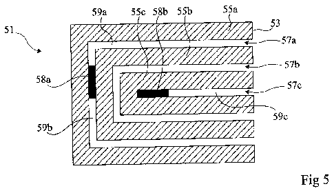
Figure 5 is a top view schematically showing a
preferred alternative embodiment of a chipless RFID tag 51. Tag
51 is formed on a dielectric support 53. One surface of support
53 supports separate parallel conductive strips in the shape of
interleaved Us. In this example, the tag comprises three conduc-
tive strips 55a to 55c, strips 55a and 55c respectively being
the outer strip and the inner strip of the pattern. The strips
are spaced apart from one another by a same step. The two paral-
lel branches of the U formed by inner strip 55c are spaced apart
by a distance equal to the step separating strips 55a to 55c
CA 02789087 2012-08-03
9
from one another. Thus, conductive strips 55a to 55c delimit two
U-shaped dielectric strips, 57a and 57b, and a rectilinear
dielectric strip 57c, between the parallel branches of the U
formed by strip 55c. Conductive bridges 58a and 58b are formed
on outer and inner dielectric strips, respectively 57a and 57c,
thus delimiting three dielectric strip portions 59a to 59c of
different lengths. To avoid stray coupling phenomena between
resonant regions of the tag, central dielectric strip 57b is not
shorted by a conductive bridge.
Tag 51 forms a structure with resonant elements capa-
ble of interfering with an electromagnetic signal transmitted by
an RFID read terminal (not shown). As in the case of the RFID
tags described in relation with Figures 3 and 4, each dielectric
strip portion 59a to 59c determines, by its length, a resonance
frequency of the tag. The tag resonance frequencies altogether
define an identification code.
Figure 6 schematically shows the spectrum of the elec-
tromagnetic signal seen by a read terminal in the presence of
tag 51 of Figure 5. The spectrum comprises three lines 59a to
59c, respectively at frequencies on the order of 2.6 GHz, 2.2
GHz, and 4.4 GHz, respectively corresponding to the resonance
frequencies linked to the dielectric strip portions having the
same reference numerals. The shorter the length of a dielectric
strip portion, the higher the associated resonance frequency.
The read terminal can detect the presence of lines in the signal
spectrum and determine the tag identification code. It should be
noted that the spectrum peaks may also be used to code the iden-
tifier associated with the tag.
Figure 7, substantially identical to Figure 5, sche-
matically shows tag 51 for three different identification codes.
The three codes correspond to three different lengths 58a1,
58a2, 58a3 of conductive bridge 58a, thus affecting the length
of dielectric strip portion 59a, as shown in dotted lines in the
drawing. Dielectric strip portions 59b and 59c have the same
length for the three codes.
CA 02789087 2012-08-03
Figure 8 schematically shows the superposition of the
power spectrums of the electromagnetic signal seen by a read
terminal in the presence of each of the tags of Figure 7. When
the length of dielectric strip portion 59a varies, the position
5 of the corresponding strip 59a in the strip also varies. The
spectrum superposition thus comprises three different strips
59al, 59a2, and 59a3, corresponding to the three different
lengths of dielectric strip portion 59a. According to an
advantage of the present invention, a length modification of one
10 of the dielectric strip portions has no influence upon the
resonance frequencies associated with the other dielectric strip
portions. Indeed, the spectrum superposition comprises a single
line 59b corresponding to the resonance frequency linked to
dielectric strip portion 59b and a single line 59c corresponding
to the resonance frequency linked to dielectric strip portion
59c. As mentioned hereabove, the spectrum peaks may also be used
to code the identifier associated with the tag.
It may be provided to associate one or several bits of
an identification code with each dielectric strip portion. As an
example, in the case of tag 51 (Figures 5 and 7), it may be
provided to associate three bits of an identification code with
each dielectric strip portion 59a to 59c. Each portion 59a to
59c may then take one of eight different lengths corresponding
to eight different resonance frequencies. It will of course be
ascertained that there is no overlapping between resonance
frequency ranges associated with different dielectric strip
portions.
Figure 9 schematically shows another alternative
embodiment of a chipless RFID tag 91. Tag 91 is similar to tag
51 of Figure 5, except for the fact that the parallel conductive
strips have the shape of concentric circle portions. The tag has
substantially the same operating principle as tag 51.
An advantage of chipless RFID tags, U-shaped or in
circle portions, of the type described in relation with Figures
5 and 9, is that they enable to store more data per surface area
unit than tags of the type described in relation with Figure 2.
CA 02789087 2012-08-03
11
As an example, tag 51 of Figure 5 enables to store a nine-bit
identification code (three bits per dielectric strip portion) on
a 17.5 x 15-mm rectangular surface, for an operating frequency
range from 2 to 5 GHz. The tag surface area can be strongly
decreased by using higher identification frequencies.
Figure 10 is a top view schematically showing another
alternative embodiment of a chipless RFID tag 101. Tag 101 is
formed on a dielectric support 103. A surface of support 103 has
parallel rectilinear conductive strips 105a to 105f formed
thereon. Strips 105a to 105f have the same width and are spaced
apart from one another by a same step. Pairs of neighboring
strips have the same length. In the shown example, neighboring
strips 105a and 105b have a first length, the next neighboring
strips 105c and 105d have a second length greater than the first
length, and the next neighboring strips 105e and 105f have a
third length greater than the second length. Thus, conductive
strips lO5a to 105d delimit three rectilinear dielectric strips
of different lengths 107a to 107c, respectively between conduc-
tive strips 105a and 105b, 105c and 105d, and 105e and 105f.
Conductive bridges 108a to 108c are formed, each at one end of
one of dielectric strips 107a to 107c, interconnecting conduc-
tive strips of same length. Actually, the configuration of
Figure 10 is similar to the configuration of Figure 3, with the
difference that parallel conductive strips have different
lengths and that the conductive bridges are formed at the end of
the dielectric strips. Each dielectric strip defines a resonant
circuit determining a resonance frequency of tag 101. The reso-
nance frequencies of the tag altogether define an identification
code.
It may be provided to associate with each dielectric
strip 107a to 107c a bit of an identification code or, as in the
example described in relation with Figure 7, several bits of an
identification code.
Specific embodiments of the present invention have
been described. Various alterations, modifications, and improve-
ments will readily occur to those skilled in the art.
CA 02789087 2012-08-03
12
In particular, chipless RFID tag patterns comprising
three or four parallel conductive strips have been described
hereabove in relation with Figures 3, 4, 5, 9, and 10. The
present invention is not limited to these specific examples.
Patterns comprising a larger number of conductive strips may
especially be provided.
Further, the possibility of associating three bits of
an identification code to each dielectric strip portion has been
mentioned. The present invention is not limited to this specific
case. It may especially be provided to associate a larger number
of bits with each dielectric strip portion. However, this will
decrease the interval, in the electromagnetic signal spectrum,
between two resonance lines corresponding to two different
lengths of a same dielectric strip portion. A sufficiently
sensitive read terminal should thus be provided.
Further, RFID tags 51, 91, and 101, described in
relation with Figures 5, 9, and 10, comprise dielectric strips
not shorted by conductive bridges to avoid stray coupling
phenomena between the resonant regions of the tag. The present
invention is not limited to this specific case. It may be
provided to use all dielectric strips for the identification
code storage, as in the case of tag 41 of Figure 4. It will then
be ascertained to provide a sufficient distance between two
dielectric strips to avoid stray coupling phenomena.
Further, in chipless RFID tags described in relation
with Figures 3, 4, 5, 9, and 10, all the dielectric strips
delimited by parallel conductive strips have the same width. The
present invention is not limited to this specific case. One may
in particular have dielectric strips of different lengths on a
same tag. Similarly, the parallel conductive strips may have
different widths.
Further, although one of the advantages of chipless
RFID tags provided hereabove is the possibility of doing away
with any conductive ground plane, one may also, for certain
uses, and especially in a metal environment, use patterns of the
CA 02789087 2012-08-03
13
type described in relation with Figures 3, 4, 5, 9, and 10 in
combination with a ground plane.