Note : Les descriptions sont présentées dans la langue officielle dans laquelle elles ont été soumises.
E 1 09 17
WO 2011/116816 PCT/EP2010/053784
1
A voltage source converter and a method for fault handling
thereof
TECHNICAL FIELD
The present invention relates to a voltage source converter having a
plurality of cell modules connected in series, each cell module
comprising a converter unit having an ac-side and a dc-side, and the
voltage source converter comprises a control unit adapted to control the
converter units. The present invention further relates to a method for
fault handling of a cell module in a voltage source converter.
BACKGROUND OF THE INVENTION
Within flexible alternating current transmission systems (FACTS) a
plurality of control apparatus are known. One such FACTS apparatus is
a static compensator (STATCOM). A STATCOM comprises a voltage
source converter (VSC) having an ac-side connected to a high voltage
transmission line or a medium voltage distribution line in an electrical
power system and a dc-side connected to a temporary electric power
storage means such as capacitors. The STATCOM transforms a dc-
voltage on its dc-side into an ac-voltage on its ac-side and can from the
power system be seen as a voltage source with variable amplitude and
phase angle. The STATCOM can supply reactive power to, or absorb
reactive power from, the transmission line or distribution line
independently of the voltage of the line.
In one type of multilevel VSC each phase includes a plurality of single
phase full-bridge converters connected in series. These single phase
full-bridge converters are sometimes referred to as chain-link cells and
are in the following denoted cell modules. In figure 1 the cell module 6
E 1 09 17
WO 2011/116816 PCT/EP2010/053784
2
includes four valves 1-4, each valve including a transistor switch, such
as an insulated gate bipolar transistor (IGBT). It is noted that other
semiconductor switching devices could be used, for example gate turn-
off thyristors (GTO) or integrated gate commutated thyristors (IGCT). A
free-wheeling diode, also denoted anti-parallel diode, is connected in
parallel with each transistor switch and conducts in the opposite
direction of the switch. The valves 1-4 are connected in an H-bridge
arrangement with a capacitor unit 5. The cell module further includes a
valve controller 11 adapted to control the valves in order to transform
a dc-voltage on its dc-side into an ac-voltage on its ac-side.
In comparison with a conventional two-level or three-level VSC,
smoother ac current and ac-voltage waveforms are possible to obtain
with lower switching frequency and minimal filtering. Each phase of the
multilevel VSC includes a number of series-connected cell modules and
a line inductor connected in series with the cell modules for current
control and filtering purposes. The number of cell modules is
proportional to the ac-voltage level of the transmission line or
distribution line to which it is connected. Consequently, the VSC can
include a large number of cell modules in series. In figure 2 is shown one
phase of such a multilevel converter connected to the high voltage
transmission line or medium voltage distribution line 7 in an electrical
power system. The phases of the VSC can be connected in a delta-
arrangement as well as in a wye-arrangement. In this example the
phase includes four cell modules 6 connected in series with a line
inductor 8. Each cell module 6 in figure 2 includes a capacitor unit 5 and
a plurality of electrical valves. The VSC includes a control unit
configured to control the valves according to a switching pattern, for
example by using a suitable pulse width modulation (PWM) technique,
in order to transform the dc-voltage on its dc-side into an ac-voltage on
its ac-side. Each valve is switched on and off a number of times during
a fundamental frequency cycle of the ac system. By controlling the
E 1 09 17
WO 2011/116816 PCT/EP2010/053784
3
timing of the switching within such fundamental frequency cycles, the
cell modules provide a desired ac-voltage, being the sum of the ac-
voltages of each cell module.
As a large number of cells may be used in series to achieve the ac-
voltage level of the transmission line or distribution line, a failure in a
single cell module could lead to a necessitated shut-down of the entire
VCS if no measures is taken. Consequently, to provide high reliability
and availability of the VSC, some type of bypass arrangement is used to
be able to continue operation of the VSC. A number of redundant cell
modules are provided to replace failed cell modules. If the system is
kept operational for the duration of a service interval, the failed
modules can be replaced during a scheduled maintenance.
To be able to bypass a faulty cell module, it is necessary to provide zero
voltage across the ac terminals of the cell. This can be achieved by
using a very fast mechanical switch, a solid-state switch or a
combination of both to allow for low power losses.
One example of a converter including a series connection of cell
modules and a short circuit device is disclosed in WO-2008/125494
where each cell module of the converter is associated with a short
circuit device, e.g. a vacuum switching tube, for short circuiting the cell
module. The short circuit device enables safe bridging of a defective cell
module.
A problem with mentioned solutions for bypassing failed cell modules is
the interruption of the load current i.e the delay between the failure of
the cell module and the bypass performed by the switch. When a cell
module fails and goes into an open circuit the load current is interrupted
which in combination with a high circuit loop inductance will result in a
E 1 09 17
WO 2011/116816 PCT/EP2010/053784
4
high voltage across the cell module and extreme energy development
which could destroy adjacent equipment.
SUMMARY OF THE INVENTION
It is an object of the invention to provide a voltage source converter
which overcome or at least alleviate the above-mentioned problems.
According to one aspect of the invention this object is achieved by a
modular energy storage device as defined in claim 1.
The voltage source converter having a plurality of cell modules
connected in series, each cell module comprising a converter unit
having an ac-side and a dc-side, and the voltage source converter
comprises a control unit adapted to control the converter units is
characterised in that at least one of the cell modules comprises a
second redundant converter unit having an ac-side which is connected
in parallel with the ac-side of the first converter unit and the control
unit is configured to synchronously control the first and the second
converter units.
The at least one cell module is formed with two identical converter
units, the ac-side of the first converter unit being connected in parallel
with the ac-side of the second redundant converter unit. Since the first
and second converter units are controlled synchronously with the same
control signals the load current will not be interrupted in case of a
failure in one of the first and second converter units and consequently
the failure does not result in a high voltage and extreme energy
development in the cell module. As a result the failed cell module will
not run a risk of destroying any adjacent equipment or jeopardizing the
continuing operation of the voltage source converter.
E 1 09 17
WO 2011/116816 PCT/EP2010/053784
In an embodiment of the invention each of the first and second
converter units includes a plurality of electrical valves and the control
unit is configured to control the valves according to a first switching
pattern during normal operation of the converter units and according to
5 a second switching pattern, having a lower switching frequency than the
first switching pattern, upon detecting a failure in one of the first and
second converter units.
Each of the first and second converter units includes a dc link capacitor
bank and a plurality of electrical valves. During the normal operation
the control unit controls the valves according to a first switching
pattern, for example by using a suitable PWM technique, in order to
transform a dc-voltage on the dc-side of the first and second converter
units into an ac-voltage on the ac-side of the first and second converter
units. Each valve is switched on and off a number of times during a
fundamental frequency cycle of the ac transmission line or distribution
line to which the voltage source converter is connected. By controlling
the timing of the switchings within said fundamental frequency cycles,
the total number of converter units will provide a desired ac-voltage of
the voltage source converter being the sum of the ac-voltages of each
cell module. During the normal operation the load current through the
voltage source converter will be uniformly, or close to uniformly, shared
between the first and second converter units, respectively.
The first and second converter units are designed with an overloading
capacity implying that each of the first and second converter units are
able to take over the current from its corresponding parallel-connected
converter unit in case of a failure in said converter unit as long as
thermal or electrical limits of the converter units are not exceeded. To
avoid excessive temperatures of the converter units, the control unit
can control the healthy, non-failed, converter unit according to the
second switching pattern with the lower switching frequency. Since the
E 1 09 17
WO 2011/116816 PCT/EP2010/053784
6
switching losses will be reduced, the moment in time when the
converter unit reaches its thermal limit will be delayed. This extra time
can be used by the control unit to identify which type of failure that has
occurred and analyse the possibility to take counteractions. There is
also a possibility that the failure is of a temporary nature which will give
an opportunity to resume the first switching pattern. This is an
advantage as the voltage source converter only has a limited number of
redundant cell modules to replace failed cell modules.
According to an embodiment of the invention the second switching
pattern is designed to control the valves to provide zero or close to zero
output voltage at the ac-side of each of the first and second converter
units. The zero output voltage can be achieved by controlling the
electrical valves of the first and second converter unit such that
forward-biased electrical valves of the first and second converter units
are switched on. Besides the zero output voltage this switching pattern
will result in a switching frequency which is equal to the fundamental
frequency of the ac transmission line or distribution line as opposed to
the first switching pattern where each valve is switched on and off a
number of times during the fundamental frequency cycle. The
advantages with this embodiment is the same as described in the
paragraph above but since the cell module provides zero or close to
zero output voltage at its ac-side, the cell module will not contribute to
the total output voltage of the voltage source converter. However, since
the switching losses is reduced to an absolute minimum the thermal
limit will be delayed to a maximum extent.
According to an embodiment of the invention the at least one cell
module further includes a bypass switch configured to bypass the cell
module upon receiving a triggering signal from the control unit.
E 1 09 17
WO 2011/116816 PCT/EP2010/053784
7
With the failure of one of the first and second converter units another
failure in the still healthy converter unit would jeopardize the
functionality of the entire voltage source converter. To avoid an
emergency shut-down of the voltage source converter, the bypass
switch is provided to bypass the load current and accordingly to ensure
a possibility to continue operation of the voltage source converter.
However, the bypass switch can be a simple mechanical closing switch
with no special requirements on speed of operation etc. owing to the
second redundant converter unit and its overloading capacity which will
ensure a maintained current path for the load current. Once the bypass
switch has been closed it will not be opened again. A mechanical bypass
switch has the advantage of low conduction losses, however
semiconductor switches such as IGBTs and MOSFETs can be used.
According to an embodiment of the invention the control unit includes a
fault detecting unit adapted to detect the presence of a failure in one of
the converter units and upon detecting that the failure has disappeared
the control unit is configured to control the valves according to the first
switching pattern. The fault detecting unit will detect the presence of a
fault based on information provided by available sensors included in the
control unit. If the failure disappears the control unit has a possibility to
resume the first switching pattern as long as the cell is not bypassed by
the bypass switch. This is an advantage since the number of redundant
cell modules is limited and there is a need for a certain number of cell
modules in operation to maintain the desired voltage level.
According to an embodiment of the invention the control unit is adapted
to generate said triggering signal to the bypass switch at a certain time
after the occurrence of a failure has been detected in any of the first
and second converter units. The load current through the still healthy
converter unit will increase after the occurrence of the failure and thus
the temperature will also increase. If said healthy converter unit
E 1 09 17
WO 2011/116816 PCT/EP2010/053784
8
exceeds its thermal limit there is a risk of a failure also in the still
healthy converter unit. On the other hand, it is an advantage to delay
the activation of the bypass switch as long as possible for reasons
mentioned above. A convenient way to accomplish such a delay is by
generating the triggering signal to the bypass switch a certain time
after the occurrence of the failure has been detected.
According to an embodiment of the invention the control unit is adapted
to generate said triggering signal to the bypass switch when the
temperature of the at least one cell module exceeds a threshold value.
By measuring the temperature of the cell module, the optimal delay of
the bypass activation switch can be more accurately determined.
According to an embodiment of the invention the voltage source
converter includes a fault detecting unit further including a dc-voltage
monitoring module adapted to continuously monitor the dc-voltage
across each of the first and second converter units and the fault
detecting module is adapted to compare the dc-voltages across the first
and second converter units and on basis thereon detect a failure in one
of the converter units.
The dc-voltages across each of the first and second converter units are
normally equal. A divergence of said dc-voltages from each other
indicates that a failure has occurred in one of the first and second
converter units. Said fault detecting module enables a faster indication
of a failure which gives the control unit extra time for analysis and
counteractions. However, it is possible that the tolerances of the
electrical ratings of the devices included in the first and second
converter units (valves, dc link capacitors etc) are such that the dc-
voltage of one of the first and second converter units differs enough
from the dc-voltage of the other parallel-connected converter unit to
indicate a failure. In one embodiment this problem is solved by the
E 1 09 17
WO 2011/116816 PCT/EP2010/053784
9
control unit by delaying the control signal to one of the first and second
converter units for up to 5 has to compensate for said tolerances and
make the dc-voltages equal or at least close to equal. Due to the very
short delay in relation to the switching frequency of the valves, the first
and second converter units can be considered as substantially
synchronously controlled. By the expression "substantially
synchronously controlled" is meant that the control signal to one of the
first or second converter unit in some situations could be slightly
delayed for a maximum of 5 has for reasons mentioned above.
According to an embodiment of the invention said at least one cell
module includes a heat sink and the first and second converter units are
thermally connected to the heat sink. Each of the first and second
converter units are preferably mounted on a base plate which in turn is
mounted on each side of the heat sink. The heat sink could be cooled
with water or forced air. The use of a common heat sink for both the
converter units will reduce the cost.
According to an embodiment of the invention the heat sink is arranged
to use forced air or deionized water as a cooling medium.
According to an embodiment of the invention said at least one cell
module is provided with a connection terminal for connection to the
next cell module in the series, and the ac-side of each of the first and
second converter units comprises an inductor in the converter unit and
connected between the ac-side of the converter unit and the connection
terminal of the cell module.
A line inductor is needed in each phase in series with the voltage source
converter for current control and filtering purposes. In this embodiment
each converter unit have a distributed inductor integrated which is also
E 1 09 17
WO 2011/116816 PCT/EP2010/053784
beneficial for parallel connected converter units in order to avoid
circulating currents between the first and second converter units due to
differences in the operation of said converter units. The integrated
inductor is preferably designed so that the need for a common line
5 inductor is eliminated completely which will reduce the cost.
According to a second aspect of the invention the object of the
invention is achieved by a method for fault handling of a cell module in
a voltage source converter as defined in claim 12.
The method for fault handling of a cell module in a voltage source
converter having a plurality of cell modules connected in series, each
cell module comprising a converter unit having an ac-side and a dc-
side, where at least one of the cell modules comprises a second
redundant converter unit having an ac-side which is connected in
parallel with the ac-side of the first converter unit is characterised by
the method steps:
- synchronously controlling the first and the second converter units,
- continuously monitoring a dc-voltage across each of the first and
second converter units of the at least one cell module,
- continuously comparing the dc-voltages across the first and second
converter units, and
- detecting a failure in one of the converter units on the basis of the
differences between the dc-voltages across the first and second
converter units.
The dc-voltages across each of the first and second converter units are
normally equal. A divergence of said dc-voltages from each other
indicates that a failure has occurred in one of the first and second
converter units. The method to continuously comparing the dc-voltages
across the first and second converter units and detecting a failure in
one of the converter units on the basis of the differences between the
E 1 09 17
WO 2011/116816 PCT/EP2010/053784
11
dc-voltages across the first and second converter units enables a faster
indication of the failure which gives the control unit extra time for
analysis and counteractions.
According to an embodiment of the invention the control unit is
configured to control one of the converter units with a delay, shorter
than 5 has, in order to keep the dc voltages across the first and second
converter unit equal or close to equal.
According to an embodiment of the invention each of the first and
second converter unit comprise a plurality of electrical valves and the
method further includes the method steps:
- controlling the valves according to a first switching pattern during
normal operation of the converter units, and
- controlling the valves according to a second switching pattern having
a lower switching frequency than the first switching pattern upon
detecting a failure in one of the first and second converter units.
Since the switching losses will be reduced, the moment in time when
the converter unit reaches its thermal limit will be delayed. This extra
time can be used by the control unit to identify which type of failure
that has occurred and analyse the possibility to take counteractions.
According to an embodiment of the invention the second switching
pattern is designed to control the valves to provide zero or close to zero
output voltage at the ac-side of each of the first and second converter
units. The advantages with this embodiment is the same as described in
the paragraph above but since the cell module provides zero or close to
zero output voltage at its ac-side, the cell module will not contribute to
the total output voltage of the voltage source converter. However, since
the switching losses are reduced to an absolute minimum the thermal
limit will be delayed to a maximum extent.
E 1 09 17
WO 2011/116816 PCT/EP2010/053784
12
According to an embodiment of the invention the method further
includes the method step:
- detecting the presence of a failure in one of the converter units and
upon detecting that the failure has disappeared controlling the valves
according to the first switching pattern.
There is a possibility that the failure is of a temporary nature which will
give the control unit an opportunity to resume the first switching
pattern. This is an advantage as the voltage source converter only has a
limited number of redundant cell modules to replace failed cell modules.
According to an embodiment of the invention the at least one cell
module further includes a bypass switch configured to bypass the cell
module upon receiving a triggering signal and the method further
includes the method step:
- generating said triggering signal to the bypass switch at a certain time
after the occurrence of a failure has been detected in any of the first
and second converter units. The load current through the still healthy
converter unit will increase after the occurrence of the failure and thus
the temperature will also increase. If said healthy converter unit
exceeds its thermal limit there is a risk of a failure also in the still
healthy converter unit. On the other hand, it is an advantage to delay
the activation of the bypass switch as long as possible for reasons
mentioned above. A convenient way to accomplish such a delay is by
generating the triggering signal to the bypass switch a certain time
after the occurrence of the failure has been detected.
According to an embodiment of the invention the at least one cell
module further includes a bypass switch configured to bypass the cell
module upon receiving a triggering signal and the method further
includes the method step:
E 1 09 17
WO 2011/116816 PCT/EP2010/053784
13
- generating said triggering signal to the bypass switch when the
temperature of the at least one cell module exceeds a threshold value.
By measuring the temperature of the cell module, the optimal delay of
the bypass activation switch can be more accurately determined.
BRIEF DESCRIPTION OF THE DRAWINGS
The present invention will be more fully described by way of example
with reference to the accompanying drawings in which:
Figure 1 shows a schematic figure of a cell module according to
prior are,
Figure 2 shows a schematic figure of one phase of a multilevel
voltage source converter according to prior are,
Figure 3 shows a schematic figure of a voltage source converter
according to an embodiment of the invention,
Figure 4 shows a detailed figure of a first example of a cell module
for a voltage source converter according to the invention,
Figure 5 shows a detailed figure of a second example of a cell
module for a voltage source converter according to the invention,
Figure 6 shows a detailed figure of a third example of a cell module
for a voltage source converter according to the invention, and
Figure 7 shows a cell module including a first and a second converter
unit mounted on a heat sink.
DETAILED DESCRIPTION OF THE INVENTION
Figure 3 illustrates a three-phase voltage source converter 22 according
to an embodiment of the invention and a high voltage transmission line
or medium voltage distribution line 7 to which the voltage source
converter is connected. The invention is however not restricted to
E 1 09 17
WO 2011/116816 PCT/EP2010/053784
14
voltage source converters having three phases. The voltage source
converter 22 can be connected in a delta or a wye arrangement. Each
phase includes a plurality of cell modules 31 and a line inductor 8
connected in series. The line inductor 8 is needed for current control
and filtering purposes. The number of cell modules varies and can be
more than one hundred. The voltage source converter 22 further
includes a control unit adapted to control the output voltage of each cell
module 31 and thus the voltage of the voltage source converter which
is the sum of the voltage of each series-connected cell module 31. The
control unit includes a main controller 70, a plurality of cell controllers
32 and a plurality of valve controllers (not shown in figure 3). The main
controller 70 sends control signals, via the cell controllers 32, to the
valve controllers in order to control the cell modules. The cell modules
31 can include any of the cell modules 15, 16 or 17 which will be
described in more detail below with references to figures 4-6. The cell
controllers 32 can include any of the cell controllers 33, 34 which also
will be described in more detail below with references to figures 4-6.
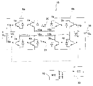
In figure 4 a first example of a cell module 15 for a voltage source
converter 22 according to the invention is illustrated. As in the prior art
each cell module 15 includes a converter unit 6a-b including a plurality
of electrical valves la-4a, lb-4b connected in an H-bridge arrangement
with a dc link capacitor bank 5a-b. Each converter unit 6a-b further
includes a valve controller 11a-b adapted to receive control signals from
the main controller 70 configured to control the valves la-4a, lb-4b
according to a first switching pattern during normal operation, for
example by using a suitable pulse width modulation (PWM) technique,
in order to transform a dc-voltage on a dc-side of the converter unit 6a-
b into an ac-voltage on an ac-side of the converter unit 6a-b. In the
first switching pattern each valve la-4a, lb-4b is switched on and off a
number of times during a fundamental frequency cycle of the line 7 to
which the voltage source converter is connected. By controlling the
E 1 09 17
WO 2011/116816 PCT/EP2010/053784
timing of the switching within such fundamental frequency cycles, each
cell module 15 provides a desired ac-voltage summing up to a total
voltage of the voltage source converter 22 being the sum of the ac-
voltages of each cell module 15.
5
The cell module 15 differs from prior art cell modules in that the cell
module 15 in addition to a first converter unit 6a includes a second
redundant converter unit 6b. The ac-sides of the first and second
converter units 6a-b are connected in parallel by connecting a first
10 connection point 10a of the first converter unit 6a with a first
connection point 10b of the second converter unit 6b and connecting a
second connection point 12a of the first converter unit 6a with a second
connection point 12b of the second converter unit 6b. The parallel-
connection of the ac-sides of the converter units 6a-b is provided with
15 connection terminals 20, 21 for connection of the cell module to the
next cell module in the series connection. An arbitrarily number of cell
modules can be connected in series in order to match the voltage level
of the line 7.
During normal operation the load current through the cell module will
be uniformly, or close to uniformly, shared between the first 6a and
second 6b converter units, respectively.
The main controller 70 sends control signals to the valve controllers
11a-b of each cell module 15 via the cell controller 33. Alternatively, the
control signals could be sent directly from the main controller 70 to the
valve controllers 11a-b. Identical control signals are received by the
valve controllers of the first and second converter units which will
control the valves to output the desired ac voltage. The first and the
second converter units are accordingly synchronously controlled. Thus,
in case of a failure in one of the first and second converter units 6a-b,
the other parallel-connected converter unit will immediately take over
E 1 09 17
WO 2011/116816 PCT/EP2010/053784
16
the load current previously flown through the failed converter unit. This
solution will prevent a high voltage and extreme energy development in
the cell module 15. As a result the failed cell module will not run a risk
of destroying any adjacent equipment or jeopardizing the continuing
operation of the voltage source converter.
As mentioned above, the valves are controlled according to the first
switching pattern during normal operation of the converter units. In
one embodiment the valves la-4a, lb-4b are controlled according to a
second switching pattern, having a lower switching frequency than the
first switching pattern, upon detecting a failure in one of the first and
second converter units 6a-b. By controlling the valves la-4a, lb-4b
according to the second switching pattern, switching losses are reduced
which means that the moment in time when the converter unit 6a-b
reaches its thermal limit will be delayed. This extra time can be used by
the control unit to identify which type of failure that has occurred and
analyse the possibility to take counteractions. There is also a possibility
that the failure is of a temporary nature and disappears which will give
an opportunity to resume the first switching pattern. This is an
advantage as the voltage source converter 22 only has a limited
number of redundant cell modules to replace failed cell modules.
In one embodiment the second switching pattern is designed to control
the valves la-4a, lb-4b to provide zero or close to zero output voltage
at the ac-side of each of the first and second converter units 6a-b. The
zero output voltage can be achieved by controlling the electrical valves
la-4a, lb-4b of the first 6a and second 6b converter unit such that
forward-biased electrical valves la-4a, lb-4b are switched on. For
example, if the current through the cell module 15 is flowing from the
connection terminal 20 to the connection terminal 21, the electrical
valves la and 4a of the converter unit 6a and the electrical valves 2b
and 3b of the converter unit 6b are switched on.
E 1 09 17
WO 2011/116816 PCT/EP2010/053784
17
Fault detecting units for detecting failures in the cell modules can be
implemented at different levels of the control unit. With different levels
is for example meant the main controller 70, the cell controller 33, 34
and the valve controller 11a-b, the main controller 70 being located on
the top level and the valve controller 11a-b being located at the bottom
level of the control unit. The fault detecting unit can for example be
implemented in the main controller 70 and failures can be detected
based on information provided by available sensors in the valves 1a-4a,
1b-4b and/or converter units 6a-b and sent to the main controller 70
for evaluation. The fault detecting unit can alternatively or additionally
be implemented in the cell controller 33, 34 or in the valve controller
11a-b. In one embodiment a dc-voltage monitoring module in the valve
controller 11a-b is adapted to continuously monitor the dc-voltage
across each of the first 6a and second 6b converter units and send
information of the dc-voltages to the fault detecting module in the cell
controller 33, 34 which is adapted to compare said dc-voltages and on
basis thereon detect a failure in one of the converter units 6a-b. The
dc-voltage monitoring module can also be implemented in other parts
of the control unit.
The dc-voltages across each of the first and second converter units are
normally equal. A divergence of said dc-voltages from each other
indicates that a failure has occurred in one of the first and second
converter units. Said fault detecting module enables a faster indication
of a failure which gives the control unit extra time for analysis and
counteractions. However, it is possible that the tolerances of the
electrical ratings of the devices included in the first and second
converter units (valves la-4a, lb-4b, dc link capacitors 5a-b etc) are
such that the dc-voltage of one of the first and second converter units
6a-b differs enough from the dc-voltage of the other parallel-connected
converter unit 6a-b to indicate a failure. In one embodiment this
E 1 09 17
WO 2011/116816 PCT/EP2010/053784
18
problem is solved by the control unit by delaying the control signal to
one of the first and second converter units 6a-b for up to 5 has to
compensate for said tolerances and make the dc-voltages equal or at
least close to equal. Due to the very short delay in relation to the
switching frequency of the valves, the first and second converter units
6a-b can be considered as substantially synchronously controlled. By
the expression "substantially synchronously controlled" is meant that
the control signal to one of the first or second converter unit in some
situations could be slightly delayed for a maximum of 5 has for reasons
mentioned above.
In figure 5 another example of a cell module 16 for the voltage source
converter according to the invention is illustrated. The same reference
numerals are used throughout the figures for same or corresponding
parts. The cell module 16 differs from the cell module 15 in that it
further includes a bypass switch 18 configured to bypass the cell
module 16 upon receiving a triggering signal from the control unit. The
triggering signal can be sent from the main controller 70 (not shown) or
via the cell controller 34.
As a result of a failure in one of the first or second converter unit 6a-b,
a second failure in the still healthy converter unit would jeopardize the
functionality of the entire voltage source converter 22. The bypass
switch 18 is provided to safely bypass the load current and accordingly
to ensure a continued operation of the voltage source converter 22. The
bypass switch 18 can be a simple mechanical closing switch without any
special requirements on speed of operation etc. owing to the second
redundant converter unit and its overloading capacity. Once the bypass
switch 18 has been closed it will not be opened again. A mechanical
bypass switch 18 has the advantage of low conduction losses, however
semiconductor switches such as IGBTs and MOSFETs can also be used.
E 1 09 17
WO 2011/116816 PCT/EP2010/053784
19
The control unit does not have to generate the triggering signal
immediately after a fault has occurred. Another possibility is to
generate said triggering signal to the bypass switch 18 a certain time
after the occurrence of a failure has been detected in any of the first
and second converter units 6a-b. it is an advantage to delay the
activation of the bypass switch 18 as long as possible as the failure can
be temporary which will give the control unit an opportunity to resume
the first switching pattern. This is an advantage as the voltage source
converter 22 only has a limited number of redundant cell modules 16 to
replace the failed cell modules 16. A convenient way to accomplish such
a delay is by generating the triggering signal to the bypass switch a
certain time after the occurrence of the failure has been detected.
Another possibility is to generate said triggering signal to the bypass
switch 18 when the temperature of the cell module 16 exceeds a
threshold value. By measuring the temperature of the cell module, an
optimal delay of the bypass switch 18 can be more accurately
determined. The triggering signal is sent from the main controller 70
via the cell controller 34, or directly from the main controller 70, based
on information provided by available temperature sensors in the valves
la-4a, lb-4b and/or converter units 6a-b.
In figure 6 yet another example of a cell module 17 for the voltage
source converter according to the invention is illustrated. The cell
module 17 differs from the cell module 15 in that it is further provided
with an inductor 19a-b in each of the converter units 30a-b and
connected between the first connection point 10a-b of the ac-side of
each converter unit 30a-b and the connection terminal 20 of the cell
module 17. Alternatively, each inductor 19a-b is connected between the
second connection point 12a-b of the ac-side of each converter unit
30a-b and the connection terminal 21 of the cell module 17.
E 1 09 17
WO 2011/116816 PCT/EP2010/053784
A line inductor 19a-b is needed in each phase in series with the cell
modules 15-17 for current limiting and filtering purposes. In this
embodiment each converter unit 30a-b has a distributed inductor. This
is also beneficial in order to avoid circulating currents between the first
5 and second converter units 30a-b due to differences in the operation of
said converter units 30a-b. The inductor 19a-b is preferably designed
such that the need for a common line inductor is eliminated completely
which will reduce the cost. The inductor can be integrated in each of the
first and second converter units or alternatively placed in the vicinity of
10 the first and second converter units.
Figure 7 shows an example of a schematic figure of the cell module 23
and a heat sink 62 thermally connected to the first and second
converter units 60a-b. In the cell module shown in figure 7 each of the
15 first and second converter units are mounted on a base plate 61a-b
which in turn is mounted on each side of the heat sink 62. The heat
sink 62 could be cooled with water or forced air flowing through holes
63 in the heat sink. The converter units 60a-b can include any of the
converter units 6ab, 30a-b. Alternatively, each of the first and second
20 converter units has a heat sink to which they are thermally connected.