Note : Les descriptions sont présentées dans la langue officielle dans laquelle elles ont été soumises.
04
1
Saint-Gobain Glass France VE1278 PCT
CO
Pane with an Electrical Connection Element
The invention relates to a pane with an electrical connection element and an
economical
and environmentally friendly method for its production.
The invention further relates to a pane with an electrical connection element
for motor
vehicles with electrically conductive structures such as, for instance,
heating conductors
or antenna conductors. The electrically conductive structures are customarily
connected
to the on-board electrical system via soldered-on electrical connection
elements. Due to
different coefficients of thermal expansion of the materials used, mechanical
stresses
occur during production and operation that strain the panes and can cause
breakage of
the pane.
Lead-containing solders have high ductility that can compensate the mechanical
stresses
occurring between an electrical connection element and the pane by plastic
deformation.
However, because of the End of Life Vehicles Directive 2000/53/EC, lead-
containing
solders have to be replaced by lead-free solders within the EC. The directive
is referred
to, in summary, by the acronym ELV (End of Life Vehicles). The objective is to
ban
extremely problematic components from products resulting from the massive
increase in
disposable electronics. The substances affected are lead, mercury, cadmium,
and
chromium. This relates, among other things, to the implementation of lead-free
soldering
materials in electrical applications on glass and the introduction of
corresponding
replacement products.
EP 1 942 703 A2 discloses an electrical connection element on panes of motor
vehicles,
wherein the difference in the coefficient of thermal expansion of a pane and
an electrical
connection element is < 5 x 10⁻⁶/ C. In order to enable adequate mechanical
stability and
processability, it is proposed to use an excess of solder material. The excess
of solder
material flows out from the intermediate space between the connection element
and the
electrically conductive structure. The excess of solder material causes high
mechanical
stresses in the glass pane. These mechanical stresses ultimately result in
breakage of the
pane.
)-04
2
Saint-Gobain Glass France VE1278 PCT
CO
The object of the present invention is to provide a pane with an electrical
connection
element and an economical and environmentally friendly method for its
production,
whereby critical mechanical stresses in the pane are avoided.
The object of the present invention is accomplished by a pane with a
connection element
that comprises the following characteristics:
- a substrate made of glass,
- an electrically conductive structure with a layer thickness of 5 pm to 40 pm
on a region of
the substrate,
- a connection element, and
- a layer of a solder material which electrically connects the connection
element to a
portion of the electrically conductive structure, wherein
- the connection element contains at least one iron-nickel alloy or one iron-
nickel-cobalt
alloy,
- the connection element is connected to the portion of the electrically
conductive structure
via a contact surface over its entire surface, and
- the contact surface has no corners.
An electrically conductive structure is applied on the pane. An electrical
connection
element is electrically connected to the electrically conductive structure by
a soldering
material on portions. The solder material flows out with an outflow width of <
1 mm from
the intermediate space between the connection element and the electrically
conductive
structure.
In a preferred embodiment, the maximum outflow width is less than 0.5 mm and,
in
particular, roughly 0 mm. The maximum outflow width can even be negative,
i.e., pulled
back into the intermediate space formed by an electrical connection element
and an
electrically conductive structure, preferably in a concave meniscus.
The maximum outflow width is defined as the distance between the outer edges
of the
connection element and the point of the solder material crossover, at which
the solder
material drops below a layer thickness of 50 pm.
The advantage resides in the reduction of mechanical stresses in the pane, in
particular,
in the critical region present with a large solder material crossover.
)-04
3
Saint-Gobain Glass France VE1278 PCT
CO
The first coefficient of thermal expansion is preferably from 8 x 10⁻⁶/ C to
9 x 10⁻⁶/ C. The substrate is preferably glass that has, preferably, a
coefficient of thermal
expansion from 8.3 x 10⁻⁶/ C to 9 x 10⁻⁶/ C in a temperature range from 0 C
to 300 C.
The second coefficient of thermal expansion is preferably from 8 x 10⁻⁶/ C to
9 x 10⁻⁶/ C, particularly preferably from 8.3 x 10⁻⁶/ C to 9 x 10⁻⁶/ C in a
temperature range
from 0 C to 300 C.
The coefficient of thermal expansion of the connection element can be <_ 4 x
10-6/ C.
The electrically conductive structure according to the invention has,
preferably, a layer
thickness of 8 pm to 15 pm, particularly preferably of 10 pm to 12 pm. The
electrically
conductive structure according to the invention contains, preferably, silver,
particularly
preferably, silver particles and glass frits.
The layer thickness of the solder according to the invention is preferably <
7.0 x 10⁻⁴ m,
particularly preferably < 3.0 x 10⁻⁴ m, and, in particular, < 0.5 x 10⁻⁴ m.
The solder material
according to the invention contains, preferably, tin and bismuth, indium,
zinc, copper,
silver, or compositions thereof. The proportion of tin in the solder
composition according to
the invention is from 3 wt.-% to 99.5 wt.-%, preferably from 10 wt.-% to 95.5
wt.-%,
particularly preferably from 15 wt.-% to 60 wt.-%. The proportion of bismuth,
indium, zinc,
copper, silver, or compositions thereof in the solder composition according to
the invention
is from 0.5 wt.-% to 97 wt.-%, preferably 10 wt.-% to 67 wt.-%, whereby the
proportion of
tin, bismuth, indium, zinc, copper, or silver can be 0 wt.-%. The solder
composition
according to the invention can contain nickel, germanium, aluminum, or
phosphorus at a
proportion of 0 wt.-% to 5 wt.-%. The solder composition according to the
invention
contains, very particularly preferably, Bi57Sn42Ag1, Bi59Sn4OAgl, ln97Ag3,
Sn95.5Ag3.8CuO.7, Bi671n33, Bi33ln50Snl7, Sn77.2ln20Ag2.8, Sn95Ag4Cu1,
Sn99Cu1,
Sn96.5Ag3.5, or mixtures thereof. The solder material according to the
invention is
preferably lead free and contains no lead or only production-related
admixtures of lead.
The connection element according to the invention contains preferably at least
50 wt.-% to
75 wt.-% iron, 25 wt.-% to 50 wt.-% nickel, 0 wt.-% to 20 wt.-% cobalt, 0 wt.-
% to
1.5 wt.-% magnesium, 0 wt.-% to 1 wt.-% silicon, 0 wt.-% to 1 wt.-% carbon, or
0 wt.-% to
1 wt.-% manganese.
)-04
4
Saint-Gobain Glass France VE1278 PCT
CO
The connection element according to the invention contains preferably
chromium,
niobium, aluminum, vanadium, tungsten, and titanium at a proportion of 0 wt.-%
to
1 wt.-%, molybdenum at a proportion of 0 wt.-% to 5 wt.-%, as well as
production-related
admixtures.
The connection element according to the invention contains preferably at least
55 wt.-% to
70 wt.-% iron, 30 wt.-% to 45 wt.-% nickel, 0 wt.-% to 5 wt.-% cobalt, 0 wt.-%
to
1 wt.-% magnesium, 0 wt.-% to 1 wt.-% silicon, or 0 wt.-% to 1 wt.-% carbon.
The connection element according to the invention further contains preferably
at least
50 wt.-% to 60 wt.-% iron, 25 wt.-% to 35 wt.-% nickel, 15 wt.-% to 20 wt.-%
cobalt,
0 wt.-% to 0.5 wt.-% silicon, 0 wt.-% to 0.1 wt.-% carbon, or 0 wt.-% to 0.5
wt.-%
manganese.
The connection element according to the invention is, particularly preferably,
partially
coated, with nickel, tin, copper, and / or silver. The connection element
according to the
invention is, very particularly preferably, coated with 0.1 pm to 0.3 pm
nickel and / or 3 pm
to 10 pm silver. The connection element can be plated with nickel, tin,
copper, and / or
silver. Ni and Ag improve the current carrying capacity and corrosion
stability of the
connection element and the wetting with the solder material.
The connection element according to the invention contains preferably kovar
(FeCoNi)
and/or invar (FeNi) with a coefficient of thermal expansion of invar of 0.1 x
10-6/ C
to 4 x 10⁻⁶/ C or a maximum difference of kovar of 5 x 10⁻⁶/ C to the
coefficient of
expansion of the pane.
Kovar is an iron-nickel-cobalt alloy that has a coefficient of thermal
expansion of usually
roughly 5 x 10⁻⁶/ C, which is thus less than the coefficient of typical
metals. The
composition contains, for example, 54 wt.-% iron, 29 wt.-% nickel, and 17 wt.-
% cobalt. In
the area of microelectronics and microsystem technology, kovar is,
consequently, used as
a housing material or as a submount. Submounts lie, according to the sandwich
principle,
between the actual carrier material and the material with, for the most part,
a clearly
greater coefficient of expansion. Kovar thus serves as a compensating element
which
absorbs and reduces the thermo-mechanical stresses caused by the different
coefficients
of thermal expansion of the other materials. Similarly, kovar is used for
metal-glass
implementations of electronic components and material transitions in vacuum
chambers.
)-04
Saint-Gobain Glass France VE1278 PCT
CO
{
Invar is an iron-nickel alloy with a content of, for example, 36 wt.-% nickel
(FeNi36). There
is a group of alloys and compounds that have the property of having abnormally
small or
sometimes negative coefficients of thermal expansion in certain temperature
ranges.
Fe65Ni35 invar contains 65 wt.-% iron and 35 wt.-% nickel. Up to 1 wt.-%
magnesium,
silicon, and carbon are usually alloyed to change the mechanical properties.
By alloying
5 wt.-% cobalt, the coefficient of thermal expansion a can be further reduced.
One name
for the alloy is Inovco, FeNi33Co4.5 with an coefficient of expansion a (20 C
to 100 C) of
0.55 x 10⁻⁶/ C.
If an alloy such as invar with a very low absolute coefficient of thermal
expansion of < 4 x
106/ C is used, overcompensation of mechanical stresses occurs through
noncritical
pressure stresses in the glass or through noncritical tensile stresses in the
alloy.
The connection element according to the invention contains preferably iron-
nickel alloys
and/or iron-nickel-cobalt-alloys post-treated thermally by annealing.
Kovar and/or invar can also be welded, crimped, or glued as a compensation
plate onto a
connection element made, for example, of steel, aluminum, titanium, copper. As
a bimetal,
favorable expansion behavior of the connection element relative to the glass
expansion
can be obtained. The compensation plate is preferably hat-shaped.
The electrical connection element contains, on the surface facing the solder
material, a
coating that contains copper, zinc, tin, silver, gold, or a combination
thereof, preferably
silver. This prevents a spreading of the solder material out beyond the
coating and limits
the outflow width.
The electrical connection element is connected over its entire surface to a
portion of the
electrically conductive structure via a contact surface. Moreover, the contact
surface of the
connection element has no corners. The contact surface can have an oval,
preferably an
elliptical, and, in particular, a circular structure. Alternatively, the
contact surface can have
a convex polygonal shape, preferably a rectangular shape, with rounded
corners. The
rounded corners have a radius of curvature of r > 0.5 mm, preferably of r > 1
mm.
)-04
6
Saint-Gobain Glass France VE1278 PCT
CO
The maximum dimensions of the connection elements are, in the plan view, for
example,
preferably 1 mm to 50 mm long and wide and, particularly preferably 3 mm to 30
mm long
and wide and, very particularly preferably 2 mm to 4 mm wide and 12 mm to 24
mm long.
The shape of the electrical connection element can form solder depots in the
intermediate
space of the connection element and the electrically conductive structure. The
solder
depots and wetting properties of the solder on the connection element prevent
the outflow
of the solder material from the intermediate space. Solder depots can be
rectangular,
rounded, or polygonal in design.
The distribution of the soldering heat and, thus, the distribution of the
solder material
during the soldering process can be defined by the shape of the connection
element.
Solder material flows to the warmest point. The introduction of energy during
the electrical
connecting of an electrical connection and an electrically conductive
structure occurs
preferably by means of punch soldering, thermode soldering, piston soldering,
preferably
laser soldering, hot air soldering, induction soldering, resistance soldering,
and/or with
ultrasound.
The object of the invention is further accomplished through a method for
producing a pane
with a connection element, wherein
a) solder material is disposed and applied on the connection element as a
platelet with a
fixed layer thickness, volume, shape, and arrangement,
b) an electrically conductive structure is applied on a substrate,
c) the connection element with the solder material is disposed on the
electrically
conductive structure, and
d) the connection element is soldered to the electrically conductive
structure.
The solder material is preferably applied in advance to the connection
elements,
preferably as a platelet with a fixed layer thickness, volume, shape, and
arrangement on
the connection element.
The connection element is welded or crimped to a (partially not shown) sheet,
braided
wire, mesh. made, for example, of copper and connected to the on-board
electrical
system (also not shown).
)-04
7
Saint-Gobain Glass France VE1278 PCT
CO
The connection element is preferably used in heated panes or in panes with
antennas in
buildings, in particular in automobiles, railroads, aircraft, or watercraft.
The connection
element serves to connect the conducting structures of the pane to electrical
systems that
are disposed outside the pane. The electrical systems are amplifiers, control
units, or
voltage sources.
The invention is explained in detail with reference to drawings and exemplary
embodiments. They depict:
Fig. 1 a plan view of a pane according to the invention with an elliptical
connection
element,
Fig. 2 a cross-section A-A' through the pane of Fig. 1,
Fig. 3 a cross-section through an alternative pane according to the invention,
Fig. 4 a cross-section through another alternative pane according to the
invention,
Fig. 5 a plan view of an alternative embodiment of the connection element,
Fig. E a plan view of another alternative embodiment of the connection
element,
Fig. 7 a plan view of another alternative embodiment of the connection
element,
Fig. 8 a side view of the connection element of Fig. 7,
Fig. 9 a cross-section through another alternative pane according to the
invention with an
arched connection element,
Fig. 10 a detailed flow chart of the method according to the invention, and
Fig. 11 a spatial representation of a connection element in the form of a
bridge.
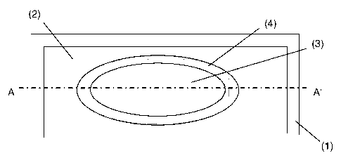
Fig.1 and Fig. 2 show, in each case, a detail of a heatable pane 1 according
to the
invention in the region of the electrical connection element 3. The pane 1 is
a 3-mm-thick
thermally prestressed single-pane safety glass made of soda-lime glass. The
pane 1 has
a width of 150 cm and a height of 80 cm. An electrically conductive structure
2 in the form
of a heating conductor structure 2 is printed on the pane 1. The electrically
conductive
structure 2 contains silver particles and glass frits. In the edge region of
the pane 1, the
electrically conductive structure 2 is widened to a width of 10 mm and forms a
contact
surface for the electrical connection element 3. In the edge region of the
pane 1, a
covering screen print (not shown) is also situated. In the region of the
contact surface
between the electrical connection element 3 and the electrically conductive
structure 2,
solder material 4 is applied, which effects a durable electrical and
mechanical connection
between the electrical connection element 3 and the electrically conductive
structure 2.
)-04
8
Saint-Gobain Glass France VE1278 PCT
CO
The solder material 4 contains 57 wt.-% bismuth, 42 wt.-% tin, and 1 wt.-%
silver. The
solder material 4 is disposed through a predefined volume and shape completely
between
the electrical connection element 3 and the electrically conductive structure
2. The solder
material 4 has a thickness of 250 pm. An outflow of the solder material 4 from
the
intermediate space between the electrical connection element 3 and the
electrically
conductive structure 2, which exceeds a layer thickness t of 50 pm, is
observed to a
maximum outflow width of b = 0.5 mm. The electrical connection element 3 is an
alloy that
contains 54 wt.-% iron, 29 wt.-% nickel, and 17 wt.-% cobalt. The electrical
connection
element 3 is designed with an elliptical base surface. The length of the major
axis is 12
mm; the length of the minor axis, 5 mm. The material thickness of the
connection element
3 is 0.8 mm. No critical mechanical stresses are observed in the pane 1 due to
the
arrangement of the solder material 4, predefined by the connection element 3
and the
electrically conductive structure 2. The connection of the pane 1 to the
electrical
connection element 3 via the electrically conductive structure 2 is durably
stable.
Fig. 3 depicts, in continuation of the exemplary embodiment of Fig. 1 and 2,
an alternative
embodiment of the connection element 3 according to the invention. The
electrical
connection element 3 is provided on the surface facing the solder material 4
with a silver-
containing coating 5. This prevents spreading of the solder material out
beyond the
coating 5 and limits the outflow width b. The outflow width b of the solder
material 4 is less
than 1 mm. No critical mechanical stresses are observed in the pane 1 due to
the
arrangement of the solder material 4. The connection of the pane 1 to the
electrical
connection element 3 via the electrically conductive structure 2 is durably
stable.
Fig. 4 depicts another embodiment of the pane 1 according to the invention
with a
connection element 3 with an elliptical base surface. The connection element 3
contains
an iron-containing alloy with a coefficient of thermal expansion of 8 x 10⁻⁶/
C. The material
thickness is 2 mm. In the region of the contact surface of the connection
element 3 with
the pane 1, a hat-shaped compensation member 6 with an iron-nickel-cobalt
alloy is
applied. The maximum layer thickness of the hat-shaped compensation member 6
is 4
mm. By means of the compensation member, it is possible to adapt the
coefficients of
thermal expansion of the connection element 3 to the requirements of the pane
1 and of
the solder material 4. The hat-shaped compensation member 6 results in
improved heat
flow during the production of the solder connection 4. The heating occurs
primarily in the
center of the contact surface. It is possible to further reduce the outflow
width b of the
solder material 4. Because of the low outflow width b of < 1 mm and the
adapted
)-04
9
Saint-Gobain Glass France VE1278 PCT
CO
coefficient of expansion, it is possible to further reduce the thermal
stresses in the pane 1.
The thermal stresses in the pane 1 are noncritical, and a durable electrical
and
mechanical connection is provided between the connection element 3 and the
pane 1 via
the electrically conductive structure 2.
Fig. 5 depicts a plan view of an alternative embodiment of the connection
element 3
according to the invention. The connection element 3 is designed as a
rectangle and has
a width of 5 mm and a length of 14 mm. The corners of the rectangle are in
each case
rounded with a circular segment with a radius of curvature r of 1 mm, for
example.
Furthermore, a connection cable 8 is welded via a welding region 7 to the
connection
element 3. The welding region 7 has a width of 3 mm and a length of 6 mm. The
connection cable 8 is a woven cable made of thin, tin-plated copper wires.
Stranded wire
cables or wires can also be used as the connection cable 8. Alternatively,
metal sleeves,
plug connectors, or crimp connections can also be electrically conductively
connected to
the connection element 3. In particular, the connection element 3 can also be
designed as
a one-piece or multi-piece clamping sleeve or crimp element.
Fig. 6 depicts a plan view of another embodiment of the connection element 3
according
to the invention. The connection element 3 is designed as a rectangle, with
the two short
sides of the rectangle designed as semicircles. The connection element has a
width of
mm and a length of 14 mm. The welding region 7 has a width of 3 mm and a
length of
6 mm.
Fig. 7 and Fig. 8 depict another embodiment of the connection element 3
according to the
invention with a connecting tab 9. The contact surface 11 of the connection
element 3 is
designed as a circle. The radius of the circle is 4 mm. The connecting tab 9
is connected
via a welding region 7 to a connection cable 8. Alternatively, the connecting
tab 9 can also
be designed as a flat plug as well as a clamping sleeve or crimp connector.
The
connecting tab 9 has, in this embodiment, two notches 10, 10'. These notches
10, 10'
serve to reduce the material of the connecting tab 9. This results in a spring
effect and
thus in the mitigation of forces that are transferred via the connection cable
8 to the solder
contact.
Fig. 9 depicts a cross-section through another embodiment of a connection
element 3
according to the invention. The connection element 3 has an arch 13 in the
center. In the
region of the curve 13, the solder material 4 is thickened.
)-04
Saint-Gobain Glass France VE1278 PCT
CO
Fig. 10 depicts in detail an example of the method according to the invention
for producing
a pane with an electrical connection element 3. As a first step, it is
necessary to portion
the solder material 4 according to shape and volume. The portioned solder
material 4 is
disposed on the electrical connection element 3. The electrical connection
element 3 is
disposed with the solder material 4 on the electrically conductive structure
2. A durable
connection of the electrical connection element 3 to the electrically
conductive structure 2
and, thus, to the pane 1 takes place through the input of energy.
Example:
Test specimens were produced with the pane 1 (thickness 3 mm, width 150 cm,
and
height 80 cm), with the electrically conductive structure 2 in the form of a
heating
conductor structure, the electrical connection element 3, the silver layer on
the contact
surfaces of the connection element 3, and the solder material 4. The solder
material 4 was
applied in advance as a platelet with fixed layer thickness, volume, and shape
on the
contact surface 11 of the connection element 3. The connection element 3 was
applied
with the solder material 4 applied on the electrically conductive structure 2.
The
connection element was soldered onto the electrically conductive structure 2
at a
temperature of 200 C and a processing time of 2 seconds. Outflow of the
solder material
4 from the intermediate space between the electrical connection element 3 and
the
electrically conductive structure 2, which exceeded a layer thickness t of 50
pm, was
observed only to a maximum outflow width of b = 0.5 mm. The dimensions and
compositions of the electrically conductive structure 2, the electrical
connection element 3,
the silver layer on the contact surfaces of the connection element 3, and the
solder
material 4 are found in Table 1 and Fig. 1 and 2 and the description of the
figures.
With all specimens, it was possible to observe, with a temperature difference
from +80 C
to -30 C, that no glass substrate 1 broke or showed damage. It was possible
to
demonstrate that, shortly after soldering, these panes 1 with the soldered
connection
element 3 were stable against a sudden temperature drop.
In addition, test specimens were executed with a second composition of the
electrical
connection element 3. The dimensions and compositions of the electrically
conductive
structure 2, the electrical connection element 3, the silver layer on the
contact surfaces of
the connection element 3, and the solder material 4 detailed values are found
in Table 2.
Here as well, it was possible to observe that, with a temperature difference
from +80 C
04
11
Saint-Gobain Glass France VE1278 PCT
CO
to -30 C, no glass substrate 1 broke or had damage. It was possible to
demonstrate that,
shortly after soldering, these panes 1 with the soldered connection element 3
were stable
against a sudden temperature drop.
Table 1
Components Material Example
Connection element
Iron 54
Nickel 29
Cobalt 17
CTE (coefficient of thermal expansion) 5.1
x10-6(0 C-100 C)
Difference between CTE of the connection 3.2
element and substrate x 10-6/ C (0 C 100 C)
Thickness of the connection element (m) 8.0 x 10
Solderable layer
Silver 100
Thickness of the layer (m) 7.0 x 10
Solder layer
Tin 42
Bismuth 57
Silver 1
Thickness of the solder layer in (m) 250 x 10
The thickness of the solderable layer and the 255 x 10
solder layer (m)
Glass substrate
(Soda lime glass)
CTE x 10 (0 C - 320 C) 8.3
)-04
12
Saint-Gobain Glass France VE1278 PCT
CO
Table 2
FComponents Material Example
Connection element
Iron 65
Nickel 35
CTE (coefficient of thermal expansion) 1.7
x 10-6 (0 C - 100 C)
Difference between CTE of the connection 6.6
element and substrate x 10-6/ C (0 C - 100 C)
Thickness of the connection element (m) 8.0 x 10⁻⁴
Solderable layer
Silver 100
Thickness of the layer (m) 7.0 x 10
Solder layer
Tin 42
Bismuth 57
Silver 1
Thickness of the solder layer in (m) 250 x 10
The thickness of the solderable layer and the 255 x 10
solder layer (m)
Glass substrate
(Soda lime glass)
CTE x 10 (0 C - 320 C) 8.3
04
13
Saint-Gobain Glass France VE1278 PCT
CO
Comparative Example 1:
The comparative example 1 was carried out the same as the example with the
following
differences: The dimensions and components of the electrically conductive
structure 2, the
electrical connection element 3, the metal layer on the contact surfaces of
the connection
element 3, and the solder material 4 are found in Table 3. The solder material
4 was, in
accordance with the prior art, not applied in advance as a platelet on the
contact surface
of the connection element 3. The connection element 3 was soldered to the
electrically
conductive structure 2 in accordance with the conventional method. With the
outflow of
the solder material 4 from the intermediate space between the electrical
connection
element 3 and the electrically conductive structure 2, which exceeded a layer
thickness t
of 50 pm, an average outflow width b = 2 mm to 3 mm was obtained.
With a sudden temperature difference from +80 C to -30 C, it was observed
that the
glass substrates 1 had major damage shortly after soldering.
)-04
14
Saint-Gobain Glass France VE1278 PCT
CO
Table 3
Components Material Comparative
Example 1
Connection element
Titanium 100
CTE (coefficient of thermal expansion) 8.80
x 10-6 (0 C -100 C)
Difference between CTE of the connection 0.5
element and substrate x 10-6/ C (0 C - 100 C)
Thickness of the connection element (m) 8.0 x 10⁻⁴
Solderable layer
Silver 100
Thickness of the layer (m) 7.0 x 10
Solder layer
Tin 48
Bismuth 46
Silver 2
Copper 4
Thickness of the solder layer in (m) 50-200 x 10
The thickness of the solderable layer and the 55-205 x 10
solder layer (m)
Glass substrate
(Soda lime glass)
CTE x 10-6(o C - 320 C) 8.3
)-04
Saint-Gobain Glass France VE1278 PCT
CO
Comparative Example 2:
The comparative example 2 was carried out the same as the example with the
following
differences. The dimensions and components of the electrically conductive
structure 2, the
electrical connection element 3, the metal layer on the contact surfaces of
the connection
element 3, and the solder material 4 are found in Table 4. The solder material
4 was, in
accordance with the prior art, not applied in advance as a platelet on the
contact surface
of the connection element 3. The connection element 3 was soldered to the
electrically
conductive structure 2 in accordance with the conventional method. With the
outflow of
the solder material 4 from the intermediate space between the electrical
connection
element 3 and the electrically conductive structure 2, which exceeded a layer
thickness
t of 50 pm, an average outflow width b = 1 mm to 1.5 mm was obtained.
With a sudden temperature difference from +80 C to -30 C, it was observed
that the
glass substrates 1 had major damage shortly after soldering.
)-04
16
Saint-Gobain Glass France VE1278 PCT
CO
Table 4
Components Material Comparative
Example 2
Connection element
Copper 100
CTE (coefficient of thermal expansion) 16
x10-6(0 C-100 C)
Difference between CTE of the connection 7.7
element and substrate x 10-6/ C (0 C - 100 C)
Thickness of the connection element (m) 8.0 x 10⁻⁴
Solderable layer
Silver 100
Thickness of the layer (m) 7.0 x 10
Solder layer
Tin 71.5
Indium 24
Silver 2.5
Bismuth 1.5
Copper 0.5
Thickness of the solder layer in (m) 50-200 x 10
The thickness of the solderable layer and the 55-205 x 10-6
solder layer (m)
Glass substrate
(Soda lime glass)
CTE x 10-6(o C - 320 C) 8.3
)-04
17
Saint-Gobain Glass France VE1278 PCT
CO
Usually, higher tensile stresses in the glass result in an increased risk of
flaking or shell
defects in the glass. Consequently, the influence of the contact surface 11
between the
connection element 3 and the portion 12 of the electrically conductive
structure 2 was
investigated by computer simulations. The tensile stresses during the cooling
of panes
with connection elements of different geometries were calculated. The various
connection
elements were bridge-shaped (B) and circular (K).
Fig. 11 depicts a perspective representation of the connection element 3 (B)
in the form of
a bridge. The connection element (B) in the form of a bridge had a width of 4
mm and a
length of 24 mm. The contact surfaces 11 of the connection element element 3
(B) in the
form of a bridge had, in each case, a width of 4 mm and a length of 6 mm. The
circular
connection element (K) had a radius of 4 mm.
A kovar alloy with a coefficient of thermal expansion a of 5.2 x 10⁻⁶/ C and
an invar alloy
with 1.7 x 10⁻⁶/ C were assumed as material for the connection elements. The
material
thickness of the connection elements was, in each case, 0.8 mm. In each case,
a glass
pane with a material thickness of 2 mm was assumed as the substrate. The
material
thickness of the solder layer 4 was, in each case, 10 pm.
In the computer simulation, the tensile stresses in the glass pane were
calculated with
cooling from +20 C to - 40 C. The maximum tensile stresses calculated are
listed in
Table 5.
Table 5
Shape of the Connection Element Maximum Tensile Stress at -40 C (MPa)
Kovar Invar
(with a = 5.2 x 10⁻⁶/ C) (with (Y. = 1.7 x 10⁻⁶/ C)
Bridge-shaped (B) 23.8 44.9
Circular (K) 12.8 24.3
The maximum tensile stresses depended strongly on the shape of the connection
element. As a result, the maximum tensile stresses in the glass pane with
circular
connection elements (K) made of kovar or invar were, in each case, 46 % less
than with
bridge-shaped connection elements (B) made of kovar or invar, cf. Table 5.
)-04
18
Saint-Gobain Glass France VE1278 PCT
CO
It was demonstrated that panes according to the invention with glass
substrates 1 and
electrical connection elements 3 according to the invention have better
stability against
sudden temperature differences.
This result was unexpected and surprising for the person skilled in the art.
)-04
19
Saint-Gobain Glass France VE1278 PCT
CO
List of Reference Characters
(1) pane / glass
(2) electrically conductive structure / Ag screenprint
(3) electrical connection element / Fe-Ni alloy Kovar
(4) solder material (Bi57Sn42Agl)
(5) wetting layer / Ag coating
(6) compensation member
(7) welding region
(8) connection cable
(9) connecting tab
(10) notch
(11) contact surface of (2) and (3)
(12) portion of (2)
(13) arch
b maximum outflow of the solder material
r radius of curvature
t limiting thickness of the solder material
A-A' section line