Note : Les descriptions sont présentées dans la langue officielle dans laquelle elles ont été soumises.
CA 02797590 2012-10-26
WO 2011/134901 PCT/EP2011/056463
1
THICK SINGLE-LENS EXTENDED
DEPTH-OF-FIELD IMAGING SYSTEMS
BACKGROUND ART
Field
[0001] The present disclosure relates generally to extended depth-of-field
imaging systems,
and particularly relates to such a system that utilizes a relatively thick
single lens element in
the imaging optical system.
Technical Background
[0002] Extended depth-of-field ("EDOF") imaging systems (also referred to as
"extended
depth-of-focus" imaging systems) have seen increased use in various
applications such as
biometrics (e.g., iris recognition), bar-code scanners and closed-circuit
television (CCTV)
systems.
[0003] The optical systems of EDOF imaging systems typically include either
more than
one lens element or include a non-circularly symmetric "wavefront coding"
plate arranged in
the entrance pupil to impart a complex wavefront shape.
[0004] Since EDOF imaging systems are desirable for use in an increasingly
greater
number of imaging applications that call for small form factors (e.g., cell
phones and other
hand-held image-capturing devices), there is a need for EDOF imaging systems
that are
extremely simple and compact but that can still provide EDOF imaging
capability with good
aberration correction.
SUMMARY
[0005] The present disclosure is directed to an extended depth-of-focus (EDOF)
imaging
system that has an optical system consisting of only one relatively thick lens
element and an
aperture stop located between front surface of the lens and the object. The
lens element is
configured so that the optical system has substantially constant spherical
aberration over the
entire image field while having substantially no coma or astigmatism, reduced
field curvature
CA 02797590 2012-10-26
WO 2011/134901 PCT/EP2011/056463
2
from prior art single-lens designs, and perhaps some chromatic aberration,
depending on the
spectral bandwidth used to form the image. The single-lens configuration makes
for a very
compact and simple EDOF imaging system useful for a wide range of imaging
applications.
[0006] It is to be understood that both the foregoing general description and
the following
detailed description present embodiments of the disclosure, and are intended
to provide an
overview or framework for understanding the nature and character of the
disclosure as it is
claimed. The accompanying drawings are included to provide a further
understanding of the
disclosure, and are incorporated into and constitute a part of this
specification. The drawings
illustrate various embodiments of the disclosure and together with the
description serve to
explain the principles and operations of the disclosure.
BRIEF DESCRIPTION OF THE DRAWINGS
[0007] FIG. 1 is a schematic diagram of an example embodiment of a single-lens
EDOF
imaging system according to the present disclosure;
[0008] FIG. 2 is a schematic diagram of an example hand-held device that
includes the
EDOF imaging system of FIG. 1, and illustrates an example controller;
[0009] FIG. 3 is a plot of the through-focus MTF for five different fields;
[0010] FIG. 4A and FIG. 4B are plots of the gain curve and the corresponding
polychromatic MTF curves, respectively, for a first example gain curve, with
the different
curves in FIG. 4B representing amounts of defocus in mm from -0.04 mm to 0.08
mm in
0.01 mm increments;
[0011] FIG. 5A and FIG. 5B are plots similar to FIG. 4A and FIG. 4B of the
gain curve
and the corresponding polychromatic MTF curves, respectively, for a second
example gain
curve;
[0012] FIG. 6A and FIG. 6B are plots similar to FIG. 4A and FIG. 4B of the
gain curve
and the corresponding polychromatic MTF curves, respectively, for a third
example gain
curve;
CA 02797590 2012-10-26
WO 2011/134901 PCT/EP2011/056463
3
[0013] FIG. 7A is a plot of an example gain curve and a target MT, and FIG. 7B
plots the
raw and processed MTF for different focus positions from - 0.04 mm to 0.08 mm
in 0.01 mm
increments, based on the gain curve of FIG. 7A;
[0014] FIG. 8 is a schematic side view of an example embodiment of a single-
lens optical
system according to the present disclosure, where the optical system includes
a thick single
lens element;
[0015] FIG. 9 plots the amount of coma (Zernike coefficient Z8) versus
aperture stop
objectwise distance from the front surface of the single lens for various
amounts of spherical
aberration;
[0016] FIG. 10 is similar to FIG. 8 and illustrates an example embodiment of
the single-
lens optical system according to Example 3;
[0017] FIGS. 11A through 11D are wavefront plots for field positions of 0 mm
(on axis),
1mm, 2mm and 3 mm for the optical system of Example 3 for wavelengths of 500
nm, 600
nm and 670 nm represented by dotted, dashed and long-dashed lines,
respectively, with the
maximum wavefront scale being +/- 2 waves;
[0018] FIG. 12A through FIG. 12F plot the focus shift (mm) as a function of
field
position for sagittal and tangential planes that illustrate the field
curvature for Examples 1
through 6, respectively
[0019] FIG. 13 plots the through-focus MTF for both the diffraction-limited
case and an
example optical system of the present disclosure, with the plot taken at line
a frequency of 33
mm'; and
[0020] FIG. 14 is the MTF plot at 6 different spatial frequencies from 10
lp/mm to 60
lp/mm versus Field on a 1/3" image sensor size of the design Example 3 that
shows the
almost constant MTF over the field.
DETAILED DESCRIPTION
[0021] Reference is now made in detail to the present preferred embodiments of
the
disclosure, examples of which are illustrated in the accompanying drawings.
Whenever
CA 02797590 2012-10-26
WO 2011/134901 PCT/EP2011/056463
4
possible, like or similar reference numerals are used throughout the drawings
to refer to like
or similar parts. Various modifications and alterations may be made to the
following
examples within the scope of the present disclosure, and aspects of the
different examples
may be mixed in different ways to achieve yet further examples. Accordingly,
the true scope
of the disclosure is to be understood from the entirety of the present
disclosure, in view of
but not limited to the embodiments described herein.
[0022] The present disclosure is directed to relatively thick single-lens EDOF
imaging
systems that cover a wide range of focal lengths and that have good correction
of field
curvature. Potential applications include compact imaging systems such as
mobile image
capture devices (e.g., cell phone cameras), iris recognition systems, facial
image capture for
facial recognition systems, CCTV systems, and the like.
[0023] The term "lens element" as used herein is defined as a single,
rotationally symmetric
optical component made of a single optical material, and does not include so-
called "phase
plates" or "phase-encoding" elements that typically reside in the entrance
pupil of an optical
system and that are not rotationally symmetric.
[0024] The phrase "extended depth-of-field" as used herein means a depth-of-
field that is
larger than what is normally associated with the corresponding diffraction-
limited optical
system. The phrase "extended depth-of-focus" is similarly defined.
[0025] The phrase "contrast-enhanced image" means an image having improved
contrast
as compared to the contrast of an initial or "raw" image formed by the optical
system.
[0026] Unless otherwise noted, the values of F/# and numerical aperture (NA)
are for the
image space.
[0027] A generalized single-lens EDOF optical imaging system is first
discussed, followed
by example embodiments of single-lens imaging optical systems for use in the
generalized
EDOF imaging system.
Generalized EDOF system
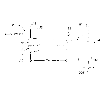
[0028] FIG. 1 is a schematic diagram of a generalized embodiment of a
generalized single-
lens EDOF optical system ("system") 10 according to the present disclosure.
System 10
CA 02797590 2012-10-26
WO 2011/134901 PCT/EP2011/056463
includes an optical axis Al along which is arranged an imaging optical system
20 that consists
of a single lens element 22 and an aperture stop AS located objectwise of the
lens element at
an axial distance DS from an objectwise front lens surface Sl. Aperture stop
AS is "clear" or
"open," meaning that it does not include any phase-altering elements, such as
phase plates,
phase-encoding optical elements or other types of phase-altering means.
[0029] Optical system 20 has a lateral magnification ML, an axial
magnification
MA = (ML)2, an object plane OP in an object space OS and an image plane IP in
an image
space IS. An object OB is shown in object plane OP and the corresponding image
IM
formed by optical system 20 is shown in image plane IP. Object OB is at an
axial object
distance DOB from lens element 22.
[0030] Optical system 20 has a depth of field DOF in object space OS over
which the
object can be imaged and remain in focus. Likewise, optical system 20 has a
corresponding
depth of focus DOF in image space IS over which image IM of object OB remains
in focus.
Object and image planes OS and IS are thus idealizations of the respective
positions of object
OB and the corresponding image IM and typically correspond to an optimum
object position
and a "best focus" position, respectively. In actuality, these planes can
actually fall anywhere
within their respective depth of field DOF and depth of focus DOF', and are
typically curved
rather than planar. The depth of field DOF and depth of focus DOF' are defined
by the
properties of optical system 20, and their interrelationship and importance in
system 10 is
discussed more fully below.
[0031] System 10 also includes an image sensor 30 that has a photosensitive
surface 32
(e.g., an array of charge-coupled devices) arranged at image plane IP so as
receive and detect
image IM, which is also referred to herein as an "initial" or a "raw" image.
In an example
embodiment, image sensor 30 is or otherwise includes a high-definition CCD
camera or
CMOS camera. In an example embodiment, photosensitive surface 32 is made up of
3000 x
2208 pixels, with a pixel size of 3.5 microns. The full-well capacity is
reduced to 21,000
electrons for a CMOS camera at this small pixel size, which translates into a
minimum of shot
noise of 43.2 dB at saturation level.
CA 02797590 2012-10-26
WO 2011/134901 PCT/EP2011/056463
6
[0032] An example image sensor 30 is or includes a camera from Pixelink PL-
A781 having
3000 x 2208 pixels linked by IEEE 1394 Fire Wire to an image processor
(discussed below),
and the application calls API provided by a Pixelink library in a DLL to
control the camera
perform image acquisition. An example image sensor 30 has about a 6 mm
diagonal
measurement of photosensitive surface 32.
[0033] In an example embodiment, system 10 further includes a controller 50,
such as a
computer or like machine, that is adapted (e.g., via instructions such as
software embodied in
a computer-readable or machine-readable medium) to control the operation of
the various
components of the system. Controller 50 is configured to control the operation
of system 10
and includes an image processing unit ("image processor") 54 electrically
connected to image
sensor 30 and adapted to receive and process digitized raw image signals SRI
therefrom and
form processed image signals SPI, as described in greater detail below.
[0034] FIG. 2 is a schematic diagram of an example hand-held device 52 that
includes
system 10, and illustrates an example controller 50. In an example embodiment,
controller 50
is or includes a computer with a processor (e.g., image processor 54) and
includes an
operating system such as Microsoft WINDOWS or LINUX.
[0035] In an example embodiment, image processor 54 is or includes any
processor or
device capable of executing a series of software instructions and includes,
without limitation,
a general- or special-purpose microprocessor, finite state machine,
controller, computer,
central-processing unit (CPU), field-programmable gate array (FPGA), or
digital signal
processor. In an example embodiment, the processor is an Intel XEON or PENTIUM
processor, or an AMD TURION or other processor in the line of such processors
made by
AMD Corp., Intel Corp. or other semiconductor processor manufacturer.
[0036] Controller 50 also preferably includes a memory unit ("memory") 110
operably
coupled to image processor 54. As used herein, the term "memory" refers to any
processor-
readable medium, including but not limited to RAM, ROM, EPROM, PROM, EEPROM,
disk, floppy disk, hard disk, CD-ROM, DVD, or the like, on which may be stored
a series of
instructions executable by image processor 54. In an example embodiment,
controller 50
CA 02797590 2012-10-26
WO 2011/134901 PCT/EP2011/056463
7
includes a port or drive 120 adapted to accommodate a removable processor-
readable
medium 116, such as CD-ROM, DVE, memory stick or like storage medium.
[0037] The EDOF methods of the present disclosure may be implemented in
various
embodiments in a machine-readable medium (e.g., memory 110) comprising machine
readable
instructions (e.g., computer programs and/or software modules) for causing
controller 50 to
perform the methods and the controlling operations for operating system 10. In
an example
embodiment, the computer programs run on image processor 54 out of memory 110,
and
may be transferred to main memory from permanent storage via disk drive or
port 120 when
stored on removable media 116, or via a network connection or modem connection
when
stored outside of controller 50, or via other types of computer or machine-
readable media
from which it can be read and utilized.
[0038] The computer programs and/or software modules may comprise multiple
modules
or objects to perform the various methods of the present disclosure, and
control the operation
and function of the various components in system 10. The type of computer
programming
languages used for the code may vary between procedural code-type languages to
object-
oriented languages. The files or objects need not have a one to one
correspondence to the
modules or method steps described depending on the desires of the programmer.
Further, the
method and apparatus may comprise combinations of software, hardware and
firmware.
Firmware can be downloaded into image processor 54 for implementing the
various example
embodiments of the disclosure.
[0039] Controller 50 also optionally includes a display 130 that can be used
to display
information using a wide variety of alphanumeric and graphical
representations. For
example, display 130 is useful for displaying enhanced images. Controller 50
also optionally
includes a data-entry device 132, such as a keyboard, that allows a user of
system 10 to input
information into controller 50 (e.g., the name of the object being imaged, and
to manually
control the operation of system 10. In an example embodiment, controller 50 is
made
sufficiently compact to fit within a small form-factor housing of a hand-held
or portable
device, such as device 52 shown in FIG. 2.
CA 02797590 2012-10-26
WO 2011/134901 PCT/EP2011/056463
8
[0040] System 10 also optionally includes a database unit 90 operably
connected to
controller 50. Database unit 90 includes a memory unit 92 that serves as a
computer-
readable medium adapted to receive processed image signals SPI from image
processor 54
and store the associated processed digital images of object OB as represented
by
the processed image signals. Memory unit ("memory") 92 may be any computer-
readable
medium, including but not limited to RAM, ROM, EPROM, PROM, EEPROM, disk,
floppy
disk, hard disk, CD-ROM, DVD, or the like, on which data may be stored. In an
example
embodiment, database unit 90 is included within controller 50.
General method of operation
[0041] With reference to FIG. 1, in the general operation of system 10, image
IM of
object OB is formed on photosensitive surface 32 of sensor 30 by optical
system 20.
Controller 50 sends a control signal S30 to activate image sensor 30 for a
given exposure
time so that image IM is captured by photosensitive surface 32. Image sensor
30 digitizes
this "raw" image IM and creates the electronic raw image signal SRI
representative of the
raw captured image.
[0042] At this point, in one example embodiment, the raw image IM can be used
directly,
i.e., without any image processing, or with only minor image processing that
does not involve
MTF-enhancement, as discussed below. This approach can be used for certain
types of
imaging applications, such as character recognition and for imaging binary
objects (e.g., bar-
code objects) where, for example, determining edge location is more important
than image
contrast. The raw image IM is associated with an EDOF provided by optical
system 20 even
without additional contrast-enhancing image processing, so that in some
example
embodiments, system 10 need not utilize the image-processing portion of the
system. In an
example embodiment, a number N of raw images are collected and averaged (e.g.,
using
image processor 54) in order to form a (digitized) raw image IM' that has
reduced noise as
compared to any one of the N raw images.
[0043] In other example embodiments where the raw image IM is not directly
usable,
image processor 54 receives and digitally processes the electronic raw image
signal SRI to
form a corresponding contrast-enhanced image embodied in an electronic
processed image
CA 02797590 2012-10-26
WO 2011/134901 PCT/EP2011/056463
9
signal SPI, which is optionally stored in database unit 90. For example, when
system 10 is
used for iris recognition, controller 50 accesses the stored processed images
in database
unit 90 and compares them to other stored iris images or to recently obtained
processed iris
images to perform personnel identification.
Image processing
[0044] Image processor 54 is adapted to receive from image sensor 30 digitized
electrical
raw image signals SRI and process the corresponding raw images to form
processed,
contrast-enhanced images. This is accomplished by filtering the raw images in
a manner that
restores the MTF as a smooth function that decreases continuously with spatial
frequency
and that preferably avoids overshoots, ringing and other image artifacts.
[0045] Noise amplification is often a problem in any filtering process that
seeks to sharpen
a signal (e.g., enhance contrast in a digital optical image). Accordingly, in
an example
embodiment, an optimized gain function (similar to Wiener's filter) that takes
in account the
power spectrum of noise is applied to reduce noise amplification during the
contrast-
enhancement process.
[0046] In an example embodiment, the gain function applied to the "raw" MTF to
form the
"output" or "enhanced" MTF (referred to hereinbelow as "output MTF' ") depends
on the
object distance DOB. The MTF versus distance DOB is acquired by a calibration
process
wherein the MTF is measured in the expected depth of field DOF by sampling
using defocus
steps (SF < (1/8)(k/(NA) to avoid any undersampling and thus the loss of
through-focus
information for the MTF. In this instance, the enhanced MTF is said to be
"focus-
dependent."
MTF restoration
[0047] The above-mentioned MTF gain function used to restore or enhance the
raw MTF
is a three-dimensional function G(u, v, d), wherein u is the spatial frequency
along the X axis,
v is the spatial frequency along the Y axis, and d is the distance of the
object in the allowed
CA 02797590 2012-10-26
WO 2011/134901 PCT/EP2011/056463
extended depth of field DOF (d thus corresponds to the object distance DOB).
The rotational
symmetry of the PSF and MTF results in a simplified definition of the gain
function, namely:
G'(cw, d) with w2 = u2 + v2
The rotational symmetry also makes G'(cw, d) a real function instead of a
complex function in
the general case.
[0048] The "enhanced" or "restored" OTF is denoted OTF' and is defined as:
OTF' (u, v, d) = G(u, v, d) OTF (u, v, d)
where OTF is the Optical Transfer Function of the optical system for
incoherent light, OTF'
is the equivalent OTF of the imaging system including the digital processing,
and G is the
aforementioned MTF gain function. The relationship for the restored or
"output" or
"enhanced" MTF (i.e., MTF) based on the original or unrestored MTF is given
by:
MTF'(cw, d) = G'(co, d) MTF (co, d)
When the object distance is unknown, an optimized average gain function G' can
be used.
The resulting MTF is enhanced, but is not a function of the object distance.
[0049] The after-digital process is preferably optimized to deliver
substantially the same
MTF at any distance in the range of the working depth of field DOF. This
provides a
substantially constant image quality, independent of object distance DOB, so
long as DOB is
within the depth of field DOF of optical system 20. Because optical system 20
has an
extended depth of field DOF due to the presence of spherical aberration as
described below,
system 10 can accommodate a relatively large variation in object distance DOB
and still be
able to capture suitable images.
[0050] FIG. 3 plots the through-focus MTF at a spatial frequency of 33 lp/mm
for
Example 3 as delivered by the optical system 20 with "white light" covering
the entire visible
spectrum.
[0051] FIGS. 4A and 4B, FIGS. 5A and 5B and FIGS. 6A and 6B plot three typical
example gain functions and their corresponding polychromatic processed
(output) MTF'
CA 02797590 2012-10-26
WO 2011/134901 PCT/EP2011/056463
11
obtained using the above-described process. The MTF gain function is
simplified as a
frequency function composed of the product of a parabolic function multiplied
by a
hypergaussian function, namely:
z
_ I f
Gain = (1 + A = f 2 )= e f
Here, A is a constant, n is the hypergaussian order, andfo is the cutoff
frequency, which is set
at the highest frequency where the raw MTF is recommended to be higher that 5%
on the
whole range of the extended depth of field DOF. The parameters A, fo and n
allows for
changing the output MTF' level and managing the cut off frequency depending of
the Nyquist
frequencyfN of the image sensor. Reducing the MTF at the Nyquist frequencyfN
reduces the
noise level and avoids aliasing artifacts in the image.
[0052] In FIG. 4A, the gain function has A = 0.003. fo = 54 and n = 1. In FIG.
5A, the
gain function has A = 0.0024. fo = 50 and n = 1.7. In FIG. 6A, the gain
function has A =
0.0016. fo=80and n=1.
[0053] FIG. 7A is a plot of an example gain curve and the output MTF' and FIG.
7B
plots the raw and processed MTFs for different focus positions (in mm, with
increments of
0.01 mm) based on the gain curve of FIG. 7A. In FIG. 7A, the shape of the
output MTF' is
as close as possible to the hypergaussian function, namely:
z
Gain (f e foZ
MTF z o (f )
[0054] In this way, the gain function is adapted to produce the hypergaussian
output MTF'
as described after the digital process. The raw MTF multiplied by the gain
function produces
the hypergaussian output MTF'.
[0055] The output MTF' is represented by a hypergaussian. The hypergaussian
output
MTF' has some valuable properties of producing a high contrast at low and
medium spatial
frequencies up to the half cut off frequency and then produces a continuous
and regular drop
CA 02797590 2012-10-26
WO 2011/134901 PCT/EP2011/056463
12
that minimize overshoot and ringing on the processed PSF, LSF (Line Spread
Function) and
ESF (Edge Spread Function).
[0056] If n = 1, the output MTF' is Gaussian. This provides a PSF, LSF and ESF
without
any ringing or overshoot. If n > 1, the output MTF' is a hypergaussian. For
higher values of
n, the contrast at high spatial frequencies is also high, but ringing and
overshoot increases. A
good compromise is 1 > n > 2, wherein the output MTF' is well enhanced at low
and medium
spatial frequencies, while the ringing and overshoot are limited to about 5%,
which is
acceptable for most imaging applications. In an example embodiment, the real
output MTF'
is as close as possible to a hypergaussian.
[0057] It is important to control the power noise amplification. At distances
where the
gain on the raw MTF is higher in order to achieve the output MTF', a good
compromise
between the MTF level and the signal-to-noise ratio on the image can be
determined, while
controlling the slope of the output MTF' at high special frequencies avoids
significant
overshoot.
[0058] In the MTF plots of FIG. 7B, the output MTF' has a smooth shape that
avoids
overshoots and other imaging artifacts. The applied gain of the digital filter
is optimized or
enhanced to obtain the maximum output MTF' while controlling the gain or
noise.
Image noise reduction by averaging sequential images
[0059] There are two distinct sources of noise associated with the image
acquisition and
image processing steps. The first source of noise is called "fixed-pattern
noise" or FP noise
for short. The FP noise is reduced by a specific calibration of image sensor
30 at the given
operating conditions. In an example embodiment, FP noise is reduced via a
multi-level
mapping of the fixed pattern noise wherein each pixel is corrected by a
calibration table, e.g.,
a lookup table that has the correction values. This requires an individual
calibration of each
image sensor and calibration data storage in a calibration file. The mapping
of the fixed
pattern noise for a given image sensor is performed, for example, by imaging a
pure white
image (e.g., from an integrating sphere) and measuring the variation in the
acquired raw
digital image.
CA 02797590 2012-10-26
WO 2011/134901 PCT/EP2011/056463
13
[0060] The other source of noise is shot noise, which is random noise. The
shot noise is
produced in electronic devices by the Poisson statistics associated with the
movement of
electrons. Shot noise also arises when converting photons to electrons via the
photo-electric
effect.
[0061] Some imaging applications, such as iris recognition, require a high-
definition image
sensor 30. To this end, in an example embodiment, image sensor 30 is or
includes a CMOS
or CCD camera having an array of 3000 x 2208 pixels with a pixel size of 3.5
gm. The full-
well capacity is reduced to 21,000 electrons for a CMOS camera at this small
pixel size, and
the associated minimum of shot noise is about 43.2 dB at the saturation level.
[0062] An example embodiment of system 10 has reduced noise so that the MTF
quality is
improved, which leads to improved images. The random nature of the shot noise
is such that
averaging N captured images is the only available approach to reducing the
noise (i.e.,
improving the SNR). The noise decreases (i.e., the SNR increases) in
proportion to N112.
This averaging process can be applied to raw images as well as to processed
(i.e., contrast-
enhanced) images.
[0063] Averaging N captured images is a suitable noise reduction approach so
long as the
images being averaged are of a fixed object or scene. However, such averaging
is
problematic when the object moves. In an example embodiment, the movement of
object OB
is tracked and accurately measured, and the averaging process for reducing
noise is employed
by accounting for and compensating for the objection motion prior to averaging
the raw
images.
[0064] In an example embodiment, the image averaging process of the present
disclosure
uses a correlation function between the sequential images at a common region
of interest.
The relative two-dimensional image shifts are determined by the location of
the correlation
peak. The correlation function is processed in the Fourier domain to speed the
calculation by
using a fast-Fourier transform (FFT) algorithm. The correlation function
provided is sampled
at the same sampling intervals as the initial images. The detection of the
correlation
maximum is accurate to the size of one pixel.
CA 02797590 2012-10-26
WO 2011/134901 PCT/EP2011/056463
14
[0065] An improvement of this measurement technique is to use a 3x3 kernel of
pixels
centered on the pixel associated with the maximum correlation peak. The sub-
pixel location
is determined by fitting to two-dimensional parabolic functions to establish a
maximum. The
(X,Y) image shift is then determined. The images are re-sampled at their
shifted locations. If
the decimal part of the measured (X,Y) shift is not equal to 0, a bi-linear
interpolation is
performed. It is also possible to use a Shannon interpolation as well because
there is no
signal in the image at frequencies higher than the Nyquist frequency. All the
images are then
summed after being re-sampled, taking in account the (X,Y) shift in the
measured correlation.
Optical System
[0066] As discussed above, imaging optical system 20 has a depth of field DOF
in object
space OS and a depth of focus DOF' in image space IS as defined by the
particular design of
the optical system. The depth of field DOF and the depth of focus DOF' for
conventional
optical imaging systems can be ascertained by measuring the evolution of the
Point Spread
Function (PSF) through focus, and can be established by specifying an amount
of loss in
resolution R that is deemed acceptable for a given application. The "circle of
least
confusion" is often taken as the parameter that defines the limit of the depth
of focus DOF'.
[0067] In the present disclosure, both the depth of field DOF and the depth of
focus
DOF' are extended by providing optical system 20 with an amount of spherical
aberration (SA). In an example embodiment, 0.22. < SA <5k, more preferably
0.22. < SA <2k and even more preferably 0.52. < SA <lk, where 2 is an imaging
wavelength.
In an example embodiment, the amount of spherical aberration SA in the optical
system at the
imaging wavelength 2 is such that the depth of field DOF or the depth of focus
DOF'
increases by an amount between 50% and 500% as compared to a diffraction
limited optical
system. By adding select amounts of spherical aberration SA, the amount of
increase in the
depth of field DOF can be controlled. The example optical system designs set
forth below
add select amounts of spherical aberration SA to increase the depth of field
DOF without
substantially increasing the adverse impact of other aberrations on image
formation.
[0068] Since the depth of field DOF and the depth of focus DOF' are related by
the axial
magnification MA and lateral magnification ML of optical system 20 via the
relationships
CA 02797590 2012-10-26
WO 2011/134901 PCT/EP2011/056463
DOF' = (MA) DOF = (ML)2 DOF, system 10 is said to have an "extended depth of
field" for
the sake of convenience. One skilled in the art will recognize that this
expression also implies
that system 10 has an "extended depth of focus" as well. Thus, either the
depth of field DOF
or the depth of focus DOF' is referred to below, depending on the context of
the discussion.
[0069] The MTF can also be used in conjunction with the PSF to characterize
the depth of
focus DOF' by examining the resolution R and image contrast Cl of the image
through focus.
Here, the image contrast is given by
Cl = (IMAX - IMIN) / (IMAX + IMIN)
and is measured for an image of a set of sinusoidal line-space pairs having a
particular spatial
frequency, where 'MAX and IMIN are the maximum and minimum image intensities,
respectively. The "best focus" is defined as the image position where the MTF
is maximized
and where the PSF is the narrowest. When an optical system is free from
aberrations (i.e., is
diffraction limited), the best focus based on the MTF coincides with the best
focus based on
the PSF. However, when aberrations are present in an optical system, the best
focus
positions based on the MTF and PSF can differ.
[0070] Conventional lens design principles call for designing an optical
system in a manner
that seeks to eliminate all aberrations, or to at least balance them to
minimize their effect so
that the optical system on the whole is substantially free of aberrations.
[0071] However, in the present disclosure, optical system 20 is intentionally
designed to
have spherical aberration as a dominant aberration, and optionally has a small
amount of
chromatic aberration as well. The spherical aberration reduces the contrast of
the image by
reducing the overall level of the MTF from the base frequencyfo = 0 to the
cutoff frequency
fc. The cut off frequencyfc is not significantly reduced as compared to the
ideal (i.e.,
diffraction-limited) MTF, so nearly all the original spatial-frequency
spectrum is available.
Thus, the spatial-frequency information is still available in the image,
albeit with a lower
contrast. The reduced contrast is then restored by the digital filtering
process as carried out
by image processing unit 54, as described above.
[0072] The amount of spherical aberration SA increases the depth of focus DOF'
in the
sense that the high spatial frequencies stay available over a greater range of
defocus. The
CA 02797590 2012-10-26
WO 2011/134901 PCT/EP2011/056463
16
digital filtering restores the contrast over the enhanced depth of focus DOF',
thereby
effectively enhancing the imaging performance of optical system 20.
[0073] Spherical aberration is an "even" aberration in the sense that the
wavefront "error"
is an even power of the normalized pupil coordinate p. Thus, spherical
aberration presents a
rotationally symmetric wavefront so that the phase is zero. This means that
the resulting
Optical Transfer Function (OTF) (which is the Fourier Transform of the PSF) is
a rotationally
symmetric, real function. The MTF, which is the magnitude of the OTF, can be
obtained
where spherical aberration is the dominant aberration by considering a one-
dimensional MTF
measurement taken on a slanted edge. This measurement provides all the
required
information to restore the two-dimensional image via digital signal
processing. Also, the
phase is zero at any defocus position, which allows for digital image
processing to enhance
the MTF without the need to consider the phase component (i.e., the phase
transfer function,
or PFT) of the OTF in the Fourier (i.e., spatial-frequency) space.
[0074] An amount of spherical aberration SA of about 0.752, gives a
significant DOF
enhancement without forming a zero in the MTF on one defocus side. Beyond
about
SA = 0.752,, a zero occurs on both sides of defocus from the best focus
position. For a
diffraction-limited optical system, the depth of focus DOF' is given by the
relationship
DOF' = 2/(NA2), where NA is the numerical aperture of the optical system. In
an example
embodiment, optical system 20 has an NA between about 0.033 and 0.125 (i.e.,
about F/15
to about F/4, where F/# = 1/(2NA) assuming the small-angle approximation).
[0075] By way of example, for F/ 6.6, a center wavelength of k = 800 nm and a
bandwidth of A2,, the diffraction-limited depth of focus DOF' is about 20mm,
with a
transverse magnification of 1/1.4. The introduction of an amount of spherical
aberration SA
= 0.75 k increases the depth of focus DOF' to about 100 mm, an increase of
about 5X.
Example optical systems with a thick single lens
[0076] One major design issue with a single-lens optical system 20 is that
control of field
curvature becomes problematic. This limits the field size or requires the use
of a field lens at
the image plane to correct the field curvature, which is often impractical
because there are
filters or windows close to image plane.
CA 02797590 2012-10-26
WO 2011/134901 PCT/EP2011/056463
17
[0077] FIG. 8 is a schematic side view of an example embodiment of a single-
lens optical
system 20 according to the present disclosure. Single lens element 22 of
optical system 20 is
relatively thick and uses a single optical material (e.g., flint glass, an
acrylic a plastic, or fused
silica) having a relatively low refractive index to facilitate field curvature
correction. An
example optical system 20 has a field size of 6 mm so that the optical system
can be used
with an image sensor 30 (see FIG. 1) having a size of 1/3 inch (diagonal
measure).
[0078] With reference to FIG. 9, control of coma (i.e., reduction or
elimination) is
accomplished by optical system 20 having a select amount of spherical
aberration SA and
then arranging aperture stop AS at a position relative to lens 22 (i.e., an
objectwise distance
DS from front surface Sl) where coma is reduced or eliminated. The presence of
spherical
aberration SA allows for a substantially constant wavefront, PSF or MTF across
the field by
removing coma. In an example, correction of field curvature and astigmatism is
accomplished using surface S2. The loss of MTF produced by the SA can be
compensated
by the signal processing techniques described above when the raw image does
not have high
enough contrast.
[0079] With reference again to FIG. 8, optical system 20 consists of single
lens element 22
arranged along optical axis Al, and aperture stop AS arranged objectwise of
the single lens
element. Lens element 20 has a front (i.e., objectwise) surface Si and a rear
(i.e.,
imagewise) surface S2, and a center (axial) thickness TH. Aperture stop AS is
arranged
along optical axis Al and defines a pupil P having a radial coordinate p.
Pupil P also defines
the optical system's entrance and exit pupils as viewed from the object and
image spaces,
respectively. In a preferred embodiment, aperture stop AS is located in object
space OB, i.e.,
anywhere between the object OB and first surface Si.
[0080] FIG. 10 is similar to FIG. 8 and illustrates an example embodiment of
optical
system 20 and single lens element 22 according to an Example 3, which is
discussed in
greater detail below. The material for lens element 22 is Poly(methyl
methacrylate) (PMMA)
having nd =1.4917 and Vd =57.44. The focal length F = 13.8 mm, the working
aperture is F/4,
the spectral range is 440 nm to 900 nm, and the field diameter is 6 mm.
CA 02797590 2012-10-26
WO 2011/134901 PCT/EP2011/056463
18
[0081] In Example 3, the aperture stop AS is located at front surface S1,
which makes
optical system 20 very compact and also makes the integration of the aperture
stop with lens
22 relatively easy. The lens thickness TH = 10 mm. Surface Si is convex and
surface S2 is
concave spherical.
[0082] The equation describing the sag of an aspheric optical surface is given
by:
2
Z - Cr +La2i.r2i
1+ ~1-(1+k~C2r 2i
where k is the conic constant, r is the radial coordinate, c is the curvature,
and a2i represents
even aspheric coefficient for i = 1, 2, 3....
[0083] Table 1 below sets forth the basic design parameters for six different
examples of
optical system 20 and lens 22. All dimensions are in millimeters. The glass
type for each lens
22 is PMMA. RI and R2 are the radii of curvature and D1 and D2 are the clear
apertures for
surfaces S1 and S2, respectively. Also, F is the focal length, F# is the F-
number, TH is the
axial thickness, TT is the "total track," which is axial thickness TH plus the
back focal length.
The FOV is the field of view, which is based on a 1/3" (6 mm) diagonal image
sensor.
EX F F# Rl Dl R2 D2 TH TT FOV
1 8 3 3.63078 4 15.1124 4 5.86227 10.1 35
2 10 3.5 3.90152 2.9325 8.48846 3.4578 6.27058 11.5 29.4
3 13.8 4 5.95515 5 22.2518 5 10.000 16.6 23.5
4 18.0 4 7.44677 4.6 20.2923 4.6 12.2306 20.7 18.25
25 4 11.3295 5.7 58.2961 6.4 18.7723 30.36 13.4
6 36 4 18.3531 7.51 320.756_F9_.26 T 29.6531 46.8 9.3
[0084] Table 2 sets forth the aspheric coefficients for surfaces Si and S2 for
the above
examples.
TABLE 2: ASPHERIC COEFFICENTS FOR EXAMPLES 1 - 6
CA 02797590 2012-10-26
WO 2011/134901 PCT/EP2011/056463
19
EX Si, S2 a4 a6 a8 a10
S1 0 0.021165631 -.012681553 0.002521543
1 S2 0.014224929 -0.0028920026 0.00063565899 -2.1174244x10⁻⁵
S1 0 0.0080693467 -0.0020410138 0
2 S2 0.0068889874 4.77189x10⁻⁵ 6.22173x10⁻⁵ 0
S1 0 0.00182174 -0.000314408 0
3 S2 0.00205553 -6.5086x10⁻⁵ 2.38613x10⁻⁵ 0
S1 0 0.00027556 -2.5834x10⁻⁵ 0
4 S2 0.0011578 -4.06548x10⁻⁵ 1.08366x10⁻⁵ 0
S1 0 3.991x10⁻⁵ -1.9259x10⁻⁶ 0
S2 0.0003166 -1.5053x10⁻⁵ 2.08375x10⁻⁶ 0
S1 0 3.991x10⁻⁵ -1.926x10⁻⁶ 0
6 S2 0.0003166 -1.5053x10⁻⁵ 2.08375x10⁻⁶ 0
[0085] Table 3 below sets forth Zernike polynomials for third-order and higher-
order
spherical aberration, and Table 4 below sets forth the Zernike coefficients
for each of
Examples 1 through 6 for on-axis and at 600 nm. The coordinate p is the
normalized radius
on the pupil 0< p <1. The term Z9 is the third- order spherical aberration
term, Z16 the fifth-
order term, etc. Note that x^n in Table 3 is shorthand notation for x".
TABLE 3 - ZERNIKE POLYNOMIALS FOR SPHERICAL ABERRATION
Z9 (6p^4 6p^2 + 1)
Z16 (20p^6 - 30p^4 + 12p^2 - 1)
Z25 (70p^8 - 140p^6 + 90p^4 - 20p^2 + 1)
Z36 (252p^10 - 630p^8 + 560p^6 - 210p^4 + 30p^2 - 1)
Z37 (924p^12 - 2772p^10 + 3150p^8 - 1680 p^6 + 420p^4 - 42p^2 + 1)
TABLE 4 - ZERNIKE POLYNOMIAL COEFFICIENTS FOR EXAMPLES 1 - 6
EX 1 EX 2 EX 3 EX 4 EX 5 EX 6
Z9 0.205 0.49545386 0.50226159 0.49634080 0.50275199 0.50484587
Z16 0.034 0.2088811 0.13286203 0.09612405 0.10575769 0.12702795
Z25 -0.153 - - - - -
0.49918268 0.29482884 0.22084578 0.22645594 0.25227367
Z36 0.225 0.00873132 0.00222264 0.00104948 - 0.00070151
0.00003476
Z37 - - - 0.00001852 0.00006942 0.00002535
0.00237 0.00009468 0.00004924
CA 02797590 2012-10-26
WO 2011/134901 PCT/EP2011/056463
[0086] FIGS. 11A through 11D are wavefront plots for field positions of 0 mm
(on axis),
1 mm, 2mm and 3 mm for the optical system 20 of Example 3. The vertical scale
is +/- 2
waves (+/-22) maximum. Three different wavelengths of 500 nm, 600 nm and 670
nm are
shown as dotted, dashed and long-dashed lines, respectively.
[0087] A characteristic of the wavefronts in FIGS. 11A through 11D is that
they show
both low-order and higher-order spherical aberration. The aspherization of
first surface S1
produces the main wavefront, with the aspherization of this surface producing
the higher-
orders of spherical aberration. Since this surface can be at or very close to
aperture stop AS
(and thus the entrance pupil), the aspherized surface S1 works much like a
phase object.
[0088] FIG. 12A through FIG. 12F plot the focus shift (mm) as a function of
field
position (normalized to 1 at the field edge) for sagittal and tangential
planes that illustrate the
field curvature for Examples 1 through 6, respectively. Because the field
curvature includes
higher-order terms, the amount of field curvature FC is defined herein as the
greatest amount
of defocus over the field relative to the on-axis field position. Said
differently, field curvature
FC is defined herein as the difference between the paraxial field curvature
and the best-focus
field curvature.
[0089] For the shortest focal length optical system 20, FC - 60 microns
(Example 6) and
for the longest focal length optical system, FC -250 microns (Example 1).
Example
embodiments of optical system 20 have field curvature FC in the range of
20 microns < FC < 300 microns.
[0090] FIG. 13 plots the through-focus MTF for both the diffraction-limited
case and the
output MTF' for an example optical system 20 having spherical aberration. The
plot is taken
at a spatial frequency of 33 mm'. Optical system 20 has been boosted by a
digital process
with a 2.5 amplification ratio applied. The depth of focus increases from 0.22
mm to 0.62
mm, an increase of 2.8X.
[0091] An important characteristic of the design of lens element 22 is that it
provides an
almost constant wavefront all over the field, thereby providing an almost
constant PSF and
MTF across the field. This is illustrated in FIG. 14, which plots the MTF vs.
field position
(mm) for a number of different spatial frequencies (from 10 lp/mm to 60 lp/mm)
for sagittal
CA 02797590 2012-10-26
WO 2011/134901 PCT/EP2011/056463
21
and tangential planes. The inclusion of higher-order spherical aberration in
optical system 20
allows for substantial enhancement of the optical system performance.
[0092] It is noted that a second parameter that has an influence on the depth
of field
determined by the through-focus MTF is chromatic aberration. A single positive
lens element
is not corrected of the chromatic aberration, the amount of which is related
to the Abbe
number of the optical material. In the present disclosure, a low- dispersion
glass or plastic is
used to minimize the loss of MTF produced by chromatic aberration.
[0093] The depth of field enhancement depends also on the required MTF or
resolution
expected for the application. For example, on a VGA camera that has 7.5 m
pixel size, the
depth of field is measured at half the Nyquist spatial frequencyfN, i.e., fN12
= 33 mm'' The
threshold of accepted MTF can thus be set at 30% contrast. In this case, the
depth of field is
the focus distance range that allows for the MTF > 30%.
Advantages
[0094] The single-element lens design of optical system 20 of EDOF system 10
has a
number of key advantages over prior art EDOF imaging systems. The first is
that the design
is simple and only uses one optical element to achieve the desired EDOF
effect. The second
is that the optical element is a standard rotationally symmetric singlet lens,
as opposed to a
more complicated phase plate. The third advantage is that configuring the
optical system to
have select amounts of spherical aberration gives rise to an axial "zero coma"
position for the
aperture stop so that comatic aberration can be substantially eliminated, with
the result that
the only significant aberration is spherical aberration uniform over the image
field-which is
what is required for the EDOF imaging. The fourth advantage is the low cost
associated
with a single-lens optical system-an advantage that cannot be overstated given
that many
applications of system 10 will be for compact devices such as CCTV cameras,
hand-held
devices such as cell phones, and like systems and devices that need to
maintain their cost
competitiveness.
[0095] It will thus be apparent to those skilled in the art that various
modifications and
variations can be made to the present disclosure without departing from the
spirit and scope
of the disclosure. Thus, it is intended that the present disclosure cover the
modifications and
CA 02797590 2012-10-26
WO 2011/134901 PCT/EP2011/056463
22
variations of this disclosure provided they come within the scope of the
appended claims and
their equivalents.