Note : Les descriptions sont présentées dans la langue officielle dans laquelle elles ont été soumises.
CA 02797754 2012-10-26
WO 2011/135504 PCT/1B2011/051773
- 1 -
METHOD AND APPARATUS FOR ADJUSTING LIGHT OUTPUT RANGE
OF SOLID STATE LIGHTING LOAD BASED ON MAXIMUM AND MINIMUM DIMMER SETTINGS
Technical Field
[0001] The present invention is directed generally to control of solid
state lighting
fixtures. More particularly, various inventive methods and apparatuses
disclosed herein relate
to adjusting a light output range of a solid state lighting system to
compensate for dimming
ranges of different dimmers.
Background
[0002] Digital or solid state lighting technologies, i.e., illumination
based on
semiconductor light sources, such as light-emitting diodes (LEDs), offer a
viable alternative to
traditional fluorescent, high-intensity discharge (HID), and incandescent
lamps. Functional
advantages and benefits of LEDs include high energy conversion and optical
efficiency,
durability, lower operating costs, and many others. Recent advances in LED
technology have
provided efficient and robust full-spectrum lighting sources that enable a
variety of lighting
effects in many applications.
[0003] Some of the fixtures embodying these sources feature a lighting
module,
including one or more LEDs capable of producing white light and/or different
colors of light,
e.g., red, green and blue, as well as a controller or processor for
independently controlling the
output of the LEDs in order to generate a variety of colors and color-changing
lighting effects,
for example, as discussed in detail in U.S. Patent Nos. 6,016,038 and
6,211,626. LED
technology includes line voltage powered luminaires, such as the
ESSENTIALWHITE series,
available from Philips Color Kinetics. Such luminaires may be dimmable using
trailing edge
dimmer technology, such as electric low voltage (ELV) type dimmers for 120VAC
line voltages
(or input mains voltages).
[0004] Many lighting applications make use of dimmers. Conventional dimmers
work
well with incandescent (bulb and halogen) lamps. However, problems occur with
other types
of electronic lamps, including compact fluorescent lamp (CFL), low voltage
halogen lamps using
CA 02797754 2012-10-26
WO 2011/135504 PCT/IB2011/051773
- 2 -
electronic transformers and solid state lighting (SSL) lamps, such as LEDs and
OLEDs. Low
voltage halogen lamps using electronic transformers, in particular, may be
dimmed using
special dimmers, such as ELV type dimmers or resistive-capacitive (RC)
dimmers, which work
adequately with loads that have a power factor correction (PFC) circuit at the
input.
[0005] Conventional dimmers typically chop a portion of each waveform of
the input
mains voltage signal and pass the remainder of the waveform to the lighting
fixture. A leading
edge or forward-phase dimmer chops the leading edge of the voltage signal
waveform. A
trailing edge or reverse-phase dimmer chops the trailing edges of the voltage
signal
waveforms. Electronic loads, such as LED drivers, typically operate better
with trailing edge
dimmers.
[0006] Unlike incandescent and other resistive lighting devices which
respond naturally
without error to a chopped sine wave produced by a phase-cutting dimmer, LEDs
and other
solid state lighting loads may incur a number of problems when placed on such
phase
chopping dimmers, such as low end drop out, triac misfiring, minimum load
issues, high end
flicker, and large steps in light output.
[0007] In addition, dimming ranges (i.e., the range between minimum and
maximum
phase angles of a dimmer) may differ from dimmer to dimmer, depending on
various factors,
such as the model and/or type of dimmer. For example, among conventional
dimmers, the
root mean square (RMS) voltage output by the dimmer and seen at an input of a
power
converter may vary from about 45 percent to about 20 percent of the full
unchopped mains at
the minimum dimmer settings (corresponding to minimum dimmer phase angles and
lowest
levels of light output), and from about 75 percent to about 95 percent of the
full unchopped
mains at the maximum dimmer settings (corresponding to maximum dimmer phase
angles and
highest levels of light output). These differences result in various dimming
levels and dimming
ranges, depending on the dimmer.
[0008] FIGs. 1A and 1B depict representative chopped waveforms of a
rectified input
mains voltage received by a power converter from different types of dimmers
(Dimmer A and
Dimmer B), respectively set at their minimum dimmer settings. As shown in
FIGs. 1A and 1B,
CA 02797754 2012-10-26
WO 2011/135504 PCT/1B2011/051773
- 3 -
the phase angle of Dimmer A at its minimum dimmer setting is larger than the
phase angle of
Dimmer B at its minimum dimmer setting. For example, Dimmer A may be a 6615-
POW
dimmer and Dimmer B may be a DVELV-303P dimmer, both available from Leviton
Manufacturing Co., in which case Dimmer A will dim down only to about 17
percent, while
Dimmer B will dim down to about 6 percent. The phase angle of each dimmer
corresponds to
an "on-time," which is the amount of time each chopped signal waveform of the
rectified input
mains voltage is non-zero. The on-time may be determined, for example, by the
amount of
time the electronic switch of the respective dimmer is "on" (i.e., enabling
current to flow to
power converter). Referring to FIGs. 1A and 1B, the on-time Tona of Dimmer A
is greater than
on-time TO b of Dimmer B.
[0009] Accordingly, Dimmer A provides a larger RMS voltage to the input to
the power
converter than Dimmer B, resulting in more light output from the solid state
lighting load
when Dimmer A is set at its minimum dimmer setting than when Dimmer B is set
at its
minimum dimmer setting. Because of the non-linear nature of the human eye's
response to
light intensity, the difference between the two lowest dimmer setting
intensities will be
dramatic. A similar situation exists with respect to the maximum dimmer
settings of Dimmer A
and Dimmer B.
Summary
[0010] The present disclosure is directed to inventive methods and devices
for
determining minimum and maximum dimmer phase angles and adjusting power output
to a
solid state lighting load based on the maximum and minimum dimmer phase angles
to control
the amount of light output by the solid state lighting load in response to the
maximum and
minimum dimmer phase angles.
[0011] Generally, in one aspect, a method is provided for controlling a
power converter
to provide a uniform dimming range to a solid state lighting load independent
of a type of
dimmer. The method includes determining maximum and minimum phase angles of a
dimmer
connected to the power converter during operation of the solid state lighting
load, and
dynamically adjusting an output power of the power converter based on the
detected
CA 02797754 2012-10-26
WO 2011/135504 PCT/1B2011/051773
- 4 -
maximum and minimum phase angles of the dimmer. The adjusted output power of
the
power converter adjusts a high end level of light output by the solid state
lighting load at the
maximum phase angle to match a predetermined high end value, and adjusts a low
end level
of light output by the solid state lighting load at the minimum phase angle to
match a
predetermined low end value.
[0012] In another aspect, a method provides a uniform dimming range of a
solid state
lighting load for multiple different types of dimmers. The method includes
initially setting a
minimum phase angle corresponding to a minimum dimmer setting and a maximum
phase
angle corresponding to maximum minimum dimmer setting; detecting a dimmer
phase angle
based on a rectified input mains voltage; determining whether the detected
phase angle is less
than the initial minimum phase angle; and setting the detected phase angle as
the minimum
phase angle when the detected phase angle is less than the initial minimum
phase angle. The
method further includes determining whether the detected phase angle is
greater than the
initial maximum phase angle; and setting the detected phase angle as the
maximum phase
angle when the detected phase angle is greater than the initial maximum phase
angle. A light
output range function is determined from the minimum phase angle and the
maximum phase
angle for determining a value of a power control signal. The power control
signal controls an
output power delivered by a power converter to the solid state lighting load,
such that the
solid state lighting load outputs a predetermined minimum light level in
response to the
minimum phase angle and outputs a predetermined maximum light level in
response to the
maximum phase angle.
[0013] In another aspect, a system is provided for controlling power
delivered to a
solid state lighting load. The system includes a power converter and a dimmer
phase angle
detection circuit. The power converter is configured to deliver a
predetermined nominal
power to the solid state light load in response to a rectified input voltage
originating from
voltage mains. The dimmer phase angle detection circuit is configured to
determine whether a
dimmer is connected between the voltage mains and the power converter, to
generate a
power control signal having a first value when the dimmer is present and
having a second
value when the dimmer is not present, and to provide the power control signal
to the power
CA 2797754 2017-04-25
81669246
- 5 -
converter. The power converter increases output power by a compensation amount
in
response to the first value of the power control signal, the increased output
power being
equal to the nominal power.
[0013a] In another aspect, there is provided a method of controlling a
power
converter to provide a uniform dimming range to a solid state lighting load
independent of a
type of dimmer, the method comprising: determining maximum and minimum phase
angles
of a dimmer connected to the power converter during operation of the solid
state lighting
load; and dynamically adjusting an output power of the power converter based
on the
detected maximum and minimum phase angles of the dimmer, the adjusted output
power of
the power converter adjusting a high end level of light output by the solid
state lighting load
at the maximum phase angle to match a predetermined high end value and
adjusting a low
end level of light output by the solid state lighting load at the minimum
phase angle to
match a predetermined low end value; determining a value of a power control
signal for
adjusting an intermediate output power of the power converter based on a
detected phase
angle of the dimmer and a function determined from said determined maximum and
minimum phase angles of the dimmer, the power control signal comprising a
pulse width
modulation (PWM) signal and the value of the power control signal comprising a
percentage
duty cycle.
10013b] In another aspect, there is provided a method for providing a
uniform
dimming range of a solid state lighting load for a plurality of different
types of dimmers, the
method comprising: initially setting a minimum phase angle corresponding to a
minimum
dimmer setting and a maximum phase angle corresponding to maximum minimum
dimmer
setting; detecting a dimmer phase angle based on a rectified input mains
voltage;
determining whether the detected phase angle is less than the initial minimum
phase angle;
setting the detected phase angle as the minimum phase angle when the detected
phase
angle is less than the initial minimum phase angle; determining whether the
detected phase
angle is greater than the initial maximum phase angle; setting the detected
phase angle as
the maximum phase angle when the detected phase angle is greater than the
initial
CA 2797754 2017-04-25
81669246
- 5a -
maximum phase angle; and determining a light output range function from the
minimum
phase angle and the maximum phase angle for determining a value of a power
control signal,
the power control signal controlling an output power delivered by a power
converter to the
solid state lighting load, such that the solid state lighting load outputs a
predetermined
minimum light level in response to the minimum phase angle and outputs a
predetermined
maximum light level in response to the maximum phase angle; determining a
value of a
power control signal for adjusting an intermediate output power of the power
converter
based on a detected phase angle of the dimmer and a function determined from
said
determined maximum and minimum phase angles of the dimmer, the power control
signal
comprising a pulse width modulation (PWM) signal and the value of the power
control signal
comprising a percentage duty cycle.
[0014] As used
herein for purposes of the present disclosure, the term "LED" should
be understood to include any electroluminescent diode or other type of carrier
injection/junction-based system that is capable of generating radiation in
response to an
electric signal. Thus, the term LED includes, but is not limited to, various
semiconductor-
based structures that emit light in response to current, light emitting
polymers, organic light
emitting diodes (OLEDs), electroluminescent strips, and the like. In
particular, the term LED
refers to light emitting diodes of all types (including semi-conductor and
organic light
emitting diodes) that may be configured to generate radiation in one or more
of the infrared
spectrum, ultraviolet spectrum, and various portions of the visible spectrum
(generally
including radiation wavelengths from approximately 400 nanometers to
approximately 700
nanometers). Some examples of LEDs include, but are not limited to, various
types of
infrared LEDs, ultraviolet LEDs, red LEDs, blue LEDs, green LEDs, yellow LEDs,
amber LEDs,
orange LEDs, and white LEDs (discussed further below). It also should be
appreciated that
LEDs may be configured and/or controlled to generate radiation having various
bandwidths
(e.g., full widths at half maximum, or FWHM) for a given spectrum (e.g.,
narrow bandwidth,
broad bandwidth), and a variety of dominant wavelengths within a given general
color
categorization.
CA 2797754 2017-04-25
81669246
- 5b -
[0015] For example, one implementation of an LED configured to generate
essentially white light (e.g., LED white lighting fixture) may include a
number of dies which
respectively emit different spectra of electroluminescence that, in
combination, mix to form
essentially white light. In another implementation, an LED white lighting
fixture may be
associated with a phosphor material that converts electroluminescence having a
first
spectrum to a different second spectrum. In one example of this
implementation,
electroluminescence having a relatively short wavelength and narrow bandwidth
spectrum
"pumps" the phosphor material, which in turn radiates longer wavelength
radiation having a
somewhat broader spectrum.
[0016] It should also be understood that the term LED does not limit the
physical
and/or electrical package type of an LED. For example, as discussed above, an
LED may refer
CA 02797754 2012-10-26
WO 2011/135504 PCT/1B2011/051773
- 6 -
to a single light emitting device having multiple dies that are configured to
respectively emit
different spectra of radiation (e.g., that may or may not be individually
controllable). Also, an
LED may be associated with a phosphor that is considered as an integral part
of the LED (e.g.,
some types of white light LEDs). In general, the term LED may refer to
packaged LEDs, non-
packaged LEDs, surface mount LEDs, chip-on-board LEDs, T-package mount LEDs,
radial
package LEDs, power package LEDs, LEDs including some type of encasement
and/or optical
element (e.g., a diffusing lens), etc.
[0017] The term "light source" should be understood to refer to any one or
more of a
variety of radiation sources, including, but not limited to, LED-based sources
(including one or
more LEDs as defined above), incandescent sources (e.g., filament lamps,
halogen lamps),
fluorescent sources, phosphorescent sources, high-intensity discharge sources
(e.g., sodium
vapor, mercury vapor, and metal halide lamps), lasers, other types of
electroluminescent
sources, pyro-luminescent sources (e.g., flames), candle-luminescent sources
(e.g., gas
mantles, carbon arc radiation sources), photo-luminescent sources (e.g.,
gaseous discharge
sources), cathode luminescent sources using electronic satiation, galvano-
luminescent sources,
crystallo-luminescent sources, kine-luminescent sources, thermo-luminescent
sources,
triboluminescent sources, sonoluminescent sources, radioluminescent sources,
and
luminescent polymers.
[0018] The term "lighting fixture" or "luminaire" is used herein to refer
to an
implementation or arrangement of one or more lighting units in a particular
form factor,
assembly, or package. The term "lighting unit" is used herein to refer to an
apparatus
including one or more light sources of same or different types. A given
lighting unit may have
any one of a variety of mounting arrangements for the light source(s),
enclosure/housing
arrangements and shapes, and/or electrical and mechanical connection
configurations.
Additionally, a given lighting unit optionally may be associated with (e.g.,
include, be coupled
to and/or packaged together with) various other components (e.g., control
circuitry) relating
to the operation of the light source(s). An "LED-based lighting unit" refers
to a lighting unit
that includes one or more LED-based light sources as discussed above, alone or
in combination
with other non LED-based light sources. A "multi-channel" lighting unit refers
to an LED-based
CA 02797754 2012-10-26
WO 2011/135504 PCT/1B2011/051773
- 7 -
or non LED-based lighting unit that includes at least two light sources
configured to
respectively generate different spectrums of radiation, wherein each different
source
spectrum may be referred to as a "channel" of the multi-channel lighting unit.
[0019] The term "controller" is used herein generally to describe various
apparatus
relating to the operation of one or more light sources. A controller can be
implemented in
numerous ways (e.g., such as with dedicated hardware) to perform various
functions discussed
herein. A "processor" is one example of a controller which employs one or more
microprocessors that may be programmed using software (e.g., microcode) to
perform various
functions discussed herein. A controller may be implemented with or without
employing a
processor, and also may be implemented as a combination of dedicated hardware
to perform
some functions and a processor (e.g., one or more programmed microprocessors
and
associated circuitry) to perform other functions. Examples of controller
components that may
be employed in various embodiments of the present disclosure include, but are
not limited to,
conventional microprocessors, microcontrollers, application specific
integrated circuits (ASICs),
and field-programmable gate arrays (FPGAs).
[0020] It should be appreciated that all combinations of the foregoing
concepts and
additional concepts discussed in greater detail below (provided such concepts
are not mutually
inconsistent) are contemplated as being part of the inventive subject matter
disclosed herein.
In particular, all combinations of claimed subject matter appearing at the end
of this disclosure
are contemplated as being part of the inventive subject matter disclosed
herein. It should also
be appreciated that terminology explicitly employed herein that also may
appear in any
disclosure incorporated by reference should be accorded a meaning most
consistent with the
particular concepts disclosed herein.
Brief Description of the Drawings
[0021] In the drawings, like reference characters generally refer to the
same or similar
parts throughout the different views. Also, the drawings are not necessarily
to scale, emphasis
instead generally being placed upon illustrating the principles of the
invention.
CA 02797754 2012-10-26
WO 2011/135504 PCT/1B2011/051773
- 8 -
[0022] FIGs. 1A-1B show waveforms of different conventional dimmers at
respective
minimum dimmer settings.
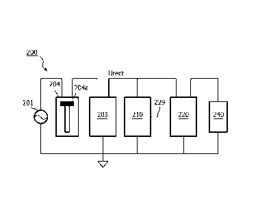
[0023] FIG. 2 is a block diagram showing a dimmable lighting system,
according to a
representative embodiment.
[0024] FIG. 3 is a flow diagram showing a process of controlling an amount
of power
delivered by a power converter to a solid state lighting load, according to a
representative
embodiment.
[0025] FIG. 4 is a flow diagram showing a process of determining maximum
and
minimum phase angles of a dimmer, according to a representative embodiment.
[0026] FIGs. 5A-5B are graphs showing dimmer phase angles versus power
control
signal values between high and low endpoints, according to a representative
embodiment.
[0027] FIG. 6 is a circuit diagram showing a control circuit for a lighting
system,
according to a representative embodiment.
[0028] FIGs. 7A-7C show sample waveforms and corresponding digital pulses
of a
dimmer, according to a representative embodiment.
[0029] FIG. 8 is a flow diagram showing a process of detecting phase
angles, according
to a representative embodiment.
Detailed Description
[0030] In the following detailed description, for purposes of explanation
and not
limitation, representative embodiments disclosing specific details are set
forth in order to
provide a thorough understanding of the present teachings. However, it will be
apparent to
one having ordinary skill in the art having had the benefit of the present
disclosure that other
embodiments according to the present teachings that depart from the specific
details
disclosed herein remain within the scope of the appended claims. Moreover,
descriptions of
well-known apparatuses and methods may be omitted so as to not obscure the
description of
the representative embodiments. Such methods and apparatuses are clearly
within the scope
of the present teachings.
CA 02797754 2012-10-26
WO 2011/135504 PCT/1B2011/051773
- 9 -
[0031] Applicants have recognized and appreciated that it would be
beneficial to
provide a circuit capable of adjusting power output by power converter to a
solid state lighting
load to compensate for differences in maximum and minimum dimming levels
provided by
different dimmers, thus providing uniform levels of high end and low end light
output by the
solid state lighting load.
[0032] Generally, it is desirable to have the same amount of light output
from a solid
state lighting load at maximum and minimum dimmer settings, respectively,
regardless of type
of dimmer (e.g., model and manufacturer) to which the solid state lighting
load is connected.
In various embodiments, maximum and minimum phase angles of a particular
dimmer are
detected during operation of the solid state lighting load. The output power
of a power
converter driving the solid state lighting load is then dynamically adjusted,
based on the
detected maximum and minimum dimmer phase angles, so that the level of light
output by the
solid state lighting load at the maximum dimmer phase angle is a predetermined
high end
value and the level of light output by the solid state lighting load at the
minimum dimmer
phase angles is a predetermined low end value.
[0033] FIG. 2 is a block diagram showing a dimmable lighting system,
including a
dimmer, dimmer phase angle detection circuit, a power converter and a solid
state lighting
fixture, according to a representative embodiment.
[0034] Referring to FIG. 2, lighting system 200 includes dimmer 204 and
rectification
circuit 205, which provide a (dimmed) rectified voltage Urect from voltage
mains 201. The
voltage mains 201 may provide different unrectified input mains voltages, such
as 100VAC,
120VAC, 230VAC and 277VAC, according to various implementations. The dimmer
204 is a
phase chopping dimmer, for example, which provides dimming capability by
chopping trailing
edges (trailing edge dimmer) or leading edges (leading edge dimmer) of voltage
signal
waveforms from the voltage mains 201 in response to vertical operation of its
slider 204a. For
purposes of discussion, it is assumed that the dimmer 204 is a trailing edge
dimmer.
[0035] Generally, the magnitude of the rectified voltage Urect is
proportional to a
phase angle or level of dimming set by the dimmer 204, such that a phase angle
corresponding
CA 2797754 2017-04-25
81669246
- 10 -
to a lower dimmer setting results in a lower rectified voltage Urect. In the
depicted example, it
may be assumed that the slider 204a is moved downward to lower the phase
angle, reducing
the amount of light output by solid state lighting load 240, and is moved
upward to increase the
phase angle, increasing the amount of light output by the solid state lighting
load 240.
Therefore, the least dimming occurs when the slider 204a is at the top
position (as depicted in
FIG. 2), and the most dimming occurs when the slider 204a is at its bottom
position.
[0036] The lighting system 200 further includes dimmer phase angle
detection
circuit 210 and power converter 220. The dimmer phase angle detection circuit
210 is
configured to determine a phase angle (dimming level) of the representative
dimmer 204
based on the rectified voltage Urect, and to adjust dynamically an operating
point of the
power converter 220 based, in part, on the determined phase angle, using a
power control
signal. The power converter 220 receives the rectified voltage Urect from the
rectification
circuit 205 and the power control signal via control line 229, and outputs a
corresponding
DC voltage for powering the solid state lighting load 240. The power converter
220 converts
between the rectified voltage Urect and the DC voltage based on at least the
magnitude of
the rectified voltage Urect and the value of the power control signal received
from the
dimmer phase angle detection circuit 210. DC voltage output by the power
converter 220
thus reflects the rectified voltage Urect and the dimmer phase angle applied
by the dimmer
204. In various embodiments, the power converter 220 operates in an open loop
or
feed-forward fashion, as described in U.S. Patent No. 7,256,554 to Lys, for
example.
[0037] In various embodiments, the power control signal may be a pulse
width
modulation (PWM) signal, for example, which alternates between high and low
levels in
accordance with a selected duty cycle. For example, the power control signal
may have a high
duty cycle (e.g., 76 percent) corresponding to a high end on-time of the
dimmer 204, and a low
duty cycle (e.g., 12 percent) corresponding to a low end on-time of the dimmer
204. When the
dimmer 204 is set in between the maximum and minimum phase angles, the dimmer
phase
angle detection circuit 210 further determines a duty cycle of the power
control signal that
CA 02797754 2012-10-26
WO 2011/135504 PCT/1B2011/051773
- 11 -
specifically corresponds to the detected dimmer phase angle, determined in
accordance with a
function adjusted for the maximum and minimum phase angles, as discussed
below.
[0038] The dimmer 204 may be one of a variety of types of phase chopping
dimmers
compatible with the solid state lighting load 240, e.g., available from
various manufacturers.
Generally, each of the different types of dimmers provides different
predetermined maximum
and minimum phase angles corresponding to the highest and lowest dimmer
settings. In other
words, the different types of dimmers have different values for the high end
on-times at
maximum dimmer settings and for the low end on-times at minimum dimmer
settings,
respectively, of the chopped sine waves, where "on-time" is the amount of time
each chopped
signal waveform of the rectified input mains voltage is non-zero, as discussed
above. Thus,
each dimmer phase angle has a corresponding on-time and vice versa. In a
conventional
lighting system, the different on-time values of the different types of
dimmers translate into
different levels of light and different dimming ranges output by the solid
state lighting load 240
in response to what otherwise appear to be the same dimmer settings.
[0039] However, according to various embodiments, the dimmer phase angle
detection circuit 210 executes an algorithm to detect the maximum phase angle
(corresponding to the high end on-time) and the minimum phase angle
(corresponding to the
low end on-time) of the particular dimmer 204, and to adjust the power control
signal, so that
the high end and low end output power delivered by the power converter 220 to
the solid
state lighting load 240 in response to the maximum and minimum phase angles of
the dimmer
204 is the same, regardless of the dimmer type. Accordingly, the levels of
light output by the
solid state lighting load 240 are likewise the same at the maximum and minimum
phase angles
of the dimmer 204, regardless of the dimmer type. Therefore, the high end and
low end light
output levels are set independently of the type of dimmer and the dimmer's
actual maximum
and minimum phase angles.
[0040] For example, when one type of dimmer has a longer high end on-time
than
another type of dimmer, the dimmer phase angle detection circuit 210 will tune
the power
control signal such that light output by the solid state lighting load 240 at
the maximum setting
of both dimmers is the same. Similarly, when one type of dimmer has a shorter
low end on-
CA 02797754 2012-10-26
WO 2011/135504 PCT/1B2011/051773
- 12 -
time than another type of dimmer, the dimmer phase angle detection circuit 210
will tune the
power control signal such that the light output by the solid state lighting
load 240 at the
minimum setting of both dimmers is the same.
[0041] FIG. 3 is a flow diagram showing a process of controlling an amount
of power
delivered by a power converter to a solid state lighting load, according to a
representative
embodiment. The process may be implemented, for example, by firmware and/or
software
executed by dimmer phase angle detection circuit 210 shown in FIG. 2, or by
microcontroller
615 of FIG. 6, discussed below.
[0042] In block S310, relationships are initially determined between
various phase
angles (dimmer on-times) and power control signal values for providing the
desired high end
and low end levels of light output by the solid state lighting load 240, when
the dimmer 204 is
set to the maximum and minimum dimmer settings, respectively. The
relationships are stored
for future access by the dimmer phase angle detection circuit 210, in order
for the dimmer
phase angle detection circuit 210 to determine an appropriate function
defining a curve
corresponding to a light output range of the solid state lighting load 240
based on maximum
and minimum dimmer phase angles and associated power control signal values,
and to
compute power control signal values corresponding to intermediate dimmer phase
angles
based on the function, as discussed below. For example, the dimmer on-times
and associated
power control signal values may be used to populate tables corresponding to
the maximum
and minimum dimmer settings, or may be saved in a relational database,
although other
means of storing the dimmer on-times and associated power control signal
values may be
incorporated without departing from the scope of the present teachings.
[0043] Initially, the desired high end and low end light output levels
(e.g., indicated in
lumens) are selected to be output by solid state lighting load 240 at the
maximum and
minimum dimmer settings, respectively. For example, a light output level of
500 lumens may
be selected as the high end level and a light output level of 25 lumens may be
selected as the
low end light level. For the selected high end light level, a value of the
power control signal is
determined for each of multiple possible high end on-times (maximum phase
angles)
corresponding to various types of dimmers, where each power control signal
value sets an
CA 02797754 2012-10-26
WO 2011/135504 PCT/1B2011/051773
- 13 -
operating point of the power converter 220 to drive the solid state lighting
load 240 to output
500 lumens in response to the high end on-time. Likewise, for the selected
minimum light
level, a value of the power control signal value is determined for each of
multiple possible low
end on-times (minimum phase angles) corresponding to the various types of
dimmers, where
each power control signal value sets an operating point of the power converter
220 to drive
the solid state lighting load 240 to output 25 lumens in response to the low
end on-time.
[0044] According to various embodiments, the power control signal values
may be
determined according to a variety of means, without departing from the scope
of the present
teachings. For example, the determined value may be a percentage of the
maximum possible
value of the power control signal. Also, the power control signal may have a
percentage duty
cycle, as discussed below, which varies from 100 percent to zero percent, in
which case the
determined power control signal value may be a percentage duty cycle within
this range. The
power control signal values may be determined empirically, for example, at the
design,
manufacturing and/or installation stage. For example, the on-times and power
control signal
of a particular dimmer may be varied to find the power control signal values
at the maximum
and minimum dimmer phase angles needed for the solid state lighting load 240
to output the
desired lumens. Alternatively, the power control signal values may be
determined
theoretically, as would be apparent to one of ordinary skill in the art,
without departing from
the scope of the present teachings.
[0045] In various embodiments, the dimmer on-times and corresponding power
control signal values for generating the high end light output level may
populate a first look-up
table, and the dimmer on-times and corresponding power control signal values
for generating
the low end light output level may populate a second look-up table. For
purposes of
discussion, Table 1 provides an example of the first look-up table, including
empirically
gathered associations between high end dimmer on-times and power control
signal values
that result in 500 lumens output by the solid state lighting load 240:
CA 02797754 2012-10-26
WO 2011/135504 PCT/1B2011/051773
- 14 -
Table 1
Dimmer On-Time Power Control Signal Lumens Out
7.0ms 90% 500
7.2ms 87% 500
7.4ms 82% 500
7.6ms 80% 500
7.8ms 78% 500
8.0ms 76% 500
8.2ms 74% 500
[0046] As discussed above, dimmer on-time is the amount of time each
chopped signal
waveform of the rectified input mains voltage is non-zero (e.g., effectively
corresponding to
the amount of time the electronic switch of the dimmer is "on"), examples of
which are shown
by Tona and Tonb in FIGs. 1A and 1B. Referring to the representative entries
in Table 1, for
example, a dimmer that outputs a signal waveform having an on-time of only
7.0ms at its
maximum setting requires a relatively large power control signal (e.g., having
a 90 percent
duty cycle) for the power converter 220 to drive the solid state lighting load
240 to output 500
lumens. In comparison, a dimmer that outputs a signal waveform having an on-
time of 8.2ms
at its maximum setting requires a relatively small power control signal (e.g.,
having a 74
percent duty cycle) for the power converter 220 to drive the solid state
lighting load 240 to
output 500 lumens. Thus, for different values of the dimmer on-times
(different RMS input
voltages to the power converter 220), the power control signal may be adjusted
so that the
output level of light is a fixed high end value at the maximum dimmer setting.
[0047] Similarly, for purposes of discussion, Table 2 provides an example
of the second
look-up table including empirically gathered associations between low end
dimmer on-times
and power control signal values that result in 25 lumens output by the solid
state lighting load
240:
CA 02797754 2012-10-26
WO 2011/135504
PCT/1B2011/051773
- 15 -
Table 2
Dimmer On-Time Power Control Signal Lumens Out
1.0ms 16% 25
1.2ms 14% 25
1.4ms 12% 25
1.6ms 10% 25
1.8ms 8% 25
2.0ms 6% 25
2.2ms 4% 25
[0048] Referring
to the representative entries in Table 2, for example, a dimmer that
outputs a signal waveform having an on-time of only 1.0ms at its minimum
setting requires a
relatively large power control signal (e.g., having a 16 percent duty cycle)
for the power
converter 220 to drive the solid state lighting load 240 to output 25 lumens.
In comparison, a
dimmer that outputs a signal waveform having an on-time of 2.2ms at its
minimum setting
requires a relatively small power control signal (e.g., having a 4 percent
duty cycle) for the
power converter 220 to drive the solid state lighting load 240 to output 25
lumens. Thus, for
different values of the dimmer on-times (different RMS input voltages to the
power converter
220), the power control signal may be adjusted so that the output level of
light is a fixed low
end value at the minimum dimmer setting.
[0049] The range
of the on-times in Tables 1 and 2 may respectively encompass the
known spreads of high end on-times and low end on-times of the dimmers
specified for a
particular product (solid state lighting load 240). In various embodiments,
Tables 1 and 2 may
be stored in the dimmer phase angle detection circuit 210, so that for a
specific high end or
low end dimmer on-time, the correct power control signal value is determined
and provided to
the power converter 220 to produce the prescribed high end or low end light
output level.
Also, although representative Tables 1 and 2 show dimmer on-times to indicate
the level of
dimming set by the dimmer, it is understood that Tables 1 and 2 could
alternatively show
dimmer phase angles to indicate the level of dimming set by the dimmer,
without departing
from the scope of the present teachings.
CA 02797754 2012-10-26
WO 2011/135504 PCT/1B2011/051773
- 16 -
[0050] Referring again to FIG. 3, in block S320, the solid state lighting
load 240 is
connected to the dimmer 204, along with the dimmer phase angle detection
circuit 210 and
the power converter 220, and operated using different dimmer settings of the
dimmer 204.
During this operation, maximum and minimum phase angles associated with the
dimmer 204
are determined by the process depicted by block S330. The determination of the
maximum
and minimum phase angles may be accomplished by dynamically detecting the
various dimmer
phase angles, and identifying the largest and smallest of the detected phase
angles (e.g.,
having the longest and shortest dimmer on-times, respectively) as the maximum
and minimum
phase angles.
[0051] FIG. 4 is a flow diagram showing a process of determining the
maximum and
minimum phase angles of a dimmer, according to a representative embodiment.
The process
may be implemented, for example, by firmware and/or software executed by
dimmer phase
angle detection circuit 210 shown in FIG. 2, or by microcontroller 615 of FIG.
6, discussed
below.
[0052] Referring to FIG. 4, an initial maximum phase angle and an initial
minimum
phase angle of the dimmer 204 are set in block S431 to begin the process. The
initial
maximum and minimum phase angles may be set to predetermined nominal values.
For
example, the initial maximum and minimum phase angles may be set to a
previously
calculated average maximum phase angle and average minimum phase angle of a
sampling of
dimmers that are compatible with the solid state lighting load 240.
Alternatively, the initial
maximum and minimum phase angles may be set to arbitrarily determined high and
low
values. Also, the initial maximum and minimum phase angles may be retrieved
from memory,
in which they were stored following prior operation of the lighting system
200, which may
avoid having to recalculate the actual maximum and minimum phase angles during
every
operation of the solid state lighting load 240.
[0053] In block S432, the dimmer phase angle is determined. For example,
the phase
angle may be detected according to the algorithm depicted in FIG. 8, discussed
below, or
retrieved from memory (e.g., in which the phase angle information was stored
in block S827 of
FIG. 8). In various embodiments, the dimmer phase angle is determined
throughout operation
CA 02797754 2012-10-26
WO 2011/135504 PCT/1B2011/051773
- 17 -
of the lighting system 200, so that any changes in the dimmer phase angle, in
response to
changes in the setting of the dimmer 204, are detected and processed.
[0054] It is determined in block S433 whether the detected phase angle is
less than the
current minimum phase angle (e.g., which is the initial minimum phase angle
during at least
the first cycle). When the currently detected phase angle is determined to be
less than the
minimum phase angle (block S433: Yes), the previous minimum phase angle is
replaced with
the currently detected phase angle in block S434. When the currently detected
phase angle is
determined not to be less than the minimum phase angle (block S433: No), the
process
proceeds to block S435, in which it is determined whether the detected phase
angle is greater
than the current maximum phase angle (e.g., the initial maximum phase angle
during at least
the first cycle).
[0055] When the currently detected phase angle is determined to be greater
than the
maximum phase angle (block S435: Yes), the previous maximum phase angle is
replaced with
the currently detected phase angle in block S436. When the currently detected
phase angle is
determined not to be greater than the minimum phase angle (block S435: No),
the process
proceeds to block S437. Of course, in alternative embodiments, the
determination of whether
the detected phase angle is greater than the current maximum phase angle may
be performed
before or simultaneously with the determination of whether the detected phase
angle is less
than the current minimum phase angle, without departing from the scope of the
present
teachings.
[0056] In block S437, the maximum and minimum phase angles of the dimmer,
as well
as the detected phase angle, are returned to the process depicted in FIG. 3.
In various
embodiments, the maximum and minimum phase angles may be returned to the
process
depicted in FIG. 3 only when changes have been made to the minimum and/or
maximum
phase angles. Otherwise, the process depicted in FIG. 3 continues using the
initial or most
recently determined maximum and minimum phase angles. The detected dimmer
phase angle
is returned so that the power control signal value can be determined to
control the output
power of the power converter 220 using a function determined from the maximum
and
minimum phase angles, as discussed below.
CA 02797754 2012-10-26
WO 2011/135504 PCT/1B2011/051773
- 18 -
[0057] Meanwhile, the phase angle detection process of FIG. 4 continues by
returning
to block S432, where the dimmer phase angle is again detected. Blocks S433
through S437 are
repeated throughout operation of the lighting system. Eventually, the dimmer
204 will be set
to its highest and lowest dimmer settings, and the corresponding actual
maximum and
minimum phase angles will be identified. However, the dimmer phase angle
detection circuit
210 will continue to generate power control signals corresponding to detected
dimmer phase
angles, as discussed below, so that dimming control may be performed on some
level, before,
during and after the actual maximum and minimum phase angles have been
determined.
[0058] Referring again to FIG. 3, in block S340, the power control signal
values
corresponding to maximum and minimum phase angles detected in the process of
block S330
are identified. This may be accomplished using the relationships between phase
angles and
power control signal values determined in block S310. For example, the maximum
and
minimum phase angles have corresponding high end and low end on-times, which
populate
previously stored first and second tables, as discussed above. For purposes of
discussion, it
may be assumed that the high end on-time has been determined to be 8.0ms and
the low end
on-time has been determined to be 1.4ms, for example. Referring to Table 1,
the power
control signal value corresponding to the high end on-time of 8.0ms is 76
percent (to yield a
light output level of 500 lumens), and referring to Table 2, the power control
signal value
corresponding to the low end on-time of 1.4ms is 12 percent (to yield a light
output level of 25
lumens).
[0059] In block S350, a function, representing the dimming range of light
output by the
solid state lighting load 240 between high and low end points corresponding to
maximum and
minimum dimmer settings, is determined using the minimum and maximum phase
angles
(high and low on-times) and the corresponding power control signal values.
Generally, any of
a variety of functions relating power control signal values to dimmer phase
angles (or on-
times) may be used in various embodiments, depending on application specific
design
requirements and desired implementations, as would be apparent to one of
ordinary skill in
the art, so long as the function has no large steps to avoid large steps in
the light output by the
solid state lighting load 240.
CA 02797754 2012-10-26
WO 2011/135504 PCT/1B2011/051773
- 19 -
[0060] FIGs. 5A and 5B show examples of "smooth" or substantially
continuous
functions relating the power control signal values (vertical axis) and dimmer
on-times
(horizontal axis), where FIG. 5A shows a linear function and FIG. 5B shows a
non-linear
function. For purposes of discussion, it may again be assumed that the high
end on-time and
corresponding power control signal value have been determined to be 8.0ms and
76 percent,
and that the low end on-time and corresponding power control signal value have
been
determined to be 1.4ms and 12 percent, for example. By correctly setting the
high end point H
and the low end point L of the function on a per dimmer basis, the high and
low light levels
corresponding to the high end point H and the low end point L can be made the
same from
dimmer to dimmer.
[0061] Although both FIGs. 5A and 5B show dimmer on-time in milliseconds,
for
purposes of explanation, it is understood that each of the on-time values has
a corresponding
dimmer phase angle, as discussed above, such that the low end on-time (e.g.,
1.4ms) has a
corresponding minimum phase angle and the high end on-time (e.g., 8.0ms) has a
corresponding maximum phase angle. Also, any function may be used to set a
desired
dimming range of light output by the solid state lighting load 240, as long as
it is smooth and
without large steps.
[0062] In block S360 of FIG. 3, a power control signal is calculated and
generated based
on the light output range function determined in block S350. Of course, if the
dimmer phase
angle detected in the process of block S330 (e.g., in block S432) is
determined to be a
maximum phase angle or a minimum phase angle, then the corresponding power
control
signal value is already known (e.g., from the first and second look-up
tables). However, for
detected dimmer phase angles between the maximum and minimum phase angles
(interim
dimmer phase angles), the value of power control signal is adjusted by the
dimmer phase
angle detection circuit 210, based on the function, such that the interim
dimmer phase angles
result in corresponding interim levels of light output by the solid state
lighting load 240. In
other words, in the examples depicted in FIGs. 5A and 5B, each of the interim
dimmer phase
angles may be plotted along the linear or non-linear curve, as a function of
the detected
dimmer phase angle (or dimmer on-time).
CA 02797754 2012-10-26
WO 2011/135504 PCT/1B2011/051773
- 20 -
[0063] The dimmer phase angle detection circuit 210 sends the power control
signal to
the power converter 220. In response, the operating point of the power
converter 220 is set,
and the power converter 220 delivers power to the solid state lighting load
240 corresponding
to the RMS input voltage and the power control signal, so that a uniformly
dimmed level of
light is output by the solid state lighting load 240 regardless of the type of
dimmer.
[0064] Thus, according to various embodiments, the dimmer phase angle
detection
circuit 210 is configured to identify the maximum and minimum phase angles of
the dimmer
204, and to output power control signals that control the power converter 220,
such that the
solid state lighting load 240 outputs a predetermined high level of light in
response to the
maximum phase angle and a predetermined low level of light in response to the
minimum
phase angle. The dimmer phase angle detection circuit 210 also outputs power
control signals
corresponding to detected interim dimmer phase angles in between the maximum
and
minimum phase angles based on a light output range function, which may be
linear or non-
linear. The dimmer phase angle detection circuit 210 outputs the power control
signal, e.g.,
via a control line 229, to the power converter 220, which dynamically adjusts
the operating
point of the power converter 220, as discussed above. Thus, the power
delivered to the solid
state lighting load 240 is determined by the RMS input voltage and the power
control signal.
[0065] FIG. 6 is a circuit diagram showing a control circuit for a lighting
system,
including a dimmer phase angle detection circuit, a power converter and a
solid state lighting
fixture, according to a representative embodiment. The general components of
FIG. 6 are
similar to those of FIG. 2, although more detail is provided with respect to
various
representative components, in accordance with an illustrative configuration.
Of course, other
configurations may be implemented without departing from the scope of the
present
teachings.
[0066] Referring to FIG. 6, control circuit 600 includes rectification
circuit 605 and
dimmer phase angle detection circuit 610 (dashed box). As discussed above with
respect to
the rectification circuit 205, the rectification circuit 605 is connected to a
dimmer connected
between the rectification circuit 605 and the voltage mains to receive
(dimmed) unrectified
voltage, indicated by the dimmed hot and neutral inputs. In the depicted
configuration, the
CA 2797754 2017-04-25
81669246
- 21 -
rectification circuit 605 includes four diodes D601-D604 connected between
rectified voltage
node N2 and ground. The rectified voltage node N2 receives the rectified
voltage Urect, and is
connected to ground through input filtering capacitor C615 connected in
parallel with the
rectification circuit 605.
[0067] The dimmer phase angle detection circuit 610 performs a phase angle
detection
process based on the rectified voltage Urect. The phase angle corresponding to
the level of
dimming set by the dimmer is detected based on the extent of phase chopping
present in a
signal waveform of the rectified voltage Urect. The dimmer phase angle
detection circuit 610
determines whether the detected phase angle is a maximum or minimum phase
angle with
respect to the particular dimmer, and generates a power control signal based
on the detected
phase angle, as discussed above. The power converter 620 controls operation of
the LED load
640, which includes representative LEDs 641 and 642 connected in series, based
on the rectified
voltage Urect (RMS input voltage) and the power control signal provided by the
dimmer phase
angle detection circuit 610. This allows the dimmer phase angle detection
circuit 610 to adjust
selectively the power delivered from the power converter 620 to the LED load
640, so that the
level of light output by the LED load 640 is substantially uniform for the
same dimmer setting
(including the high end and low end settings) among a variety of different
types of dimmers. In
various embodiments, the power converter 620 operates in an open loop or feed-
forward
fashion, as described in U.S. Patent No. 7,256,554 to Lys, for example.
[0068] In the depicted representative embodiment, the dimmer phase angle
detection
circuit 610 includes microcontroller 615, which uses signal waveforms of the
rectified voltage
Urect to determine the phase angle. The microcontroller 615 includes digital
input 618
connected between a first diode D611 and a second diode D612. The first diode
D611 has an
anode connected to the digital input 618 and a cathode connected to voltage
source Vcc, and
the second diode D612 has an anode connected to ground and a cathode connected
to the
digital input 618. The microcontroller 615 also includes the digital output
619.
[0069] In various embodiments, the microcontroller 615 may be a PIC12F683
processor,
available from Microchip Technology, Inc., and the power converter 620 may be
an
CA 02797754 2012-10-26
WO 2011/135504 PCT/1B2011/051773
- 22 -
L6562, available from ST Microelectronics, for example, although other types
of
microcontrollers, power converters, or other processors and/or controllers may
be included
without departing from the scope of the present teachings. For example, the
functionality of
the microcontroller 615 may be implemented by one or more processors and/or
controllers,
connected to receive digital input between first and second diodes D611 and
D612 as
discussed above, and which may be programmed using software or firmware (e.g.,
stored in a
memory) to perform the various functions described herein, or may be
implemented as a
combination of dedicated hardware to perform some functions and a processor
(e.g., one or
more programmed microprocessors and associated circuitry) to perform other
functions.
Examples of controller components that may be employed in various embodiments
include,
but are not limited to, conventional microprocessors, microcontrollers, ASICs
and FPGAs, as
discussed above.
[0070] The dimmer phase angle detection circuit 610 further includes
various passive
electronic components, such as first and second capacitors C613 and C614, and
a resistance
indicated by representative first and second resistors R611 and R612. The
first capacitor C613
is connected between the digital input 618 of the microcontroller 615 and a
detection node
Ni. The second capacitor C614 is connected between the detection node Ni and
ground. The
first and second resistors R611 and R612 are connected in series between the
rectified voltage
node N2 and the detection node Ni. In the depicted embodiment, the first
capacitor C613
may have a value of about 560pF and the second capacitor C614 may have a value
of about
10pF, for example. Also, the first resistor R611 may have a value of about 1
megohm and the
second resistor R612 may have a value of about 1 megohm, for example. However,
the
respective values of the first and second capacitors C613 and C614, and the
first and second
resistors R611 and R612 may vary to provide unique benefits for any particular
situation or to
meet application specific design requirements of various implementations, as
would be
apparent to one of ordinary skill in the art.
[0071] The rectified voltage Urect is AC coupled to the digital input 618
of the
microcontroller 615. The first resistor R611 and the second resistor R612
limit the current into
the digital input 618. When a signal waveform of the rectified voltage Urect
goes high, the
CA 02797754 2012-10-26
WO 2011/135504 PCT/1B2011/051773
- 23 -
first capacitor C613 is charged on the rising edge through the first and
second resistors R611
and R612. The first diode D611 clamps the digital input 618 one diode drop
above the voltage
source Vcc, for example, while the first capacitor C613 is charged. The first
capacitor C613
remains charged as long as the signal waveform is not zero. On the falling
edge of the signal
waveform of the rectified voltage Urect, the first capacitor C613 discharges
through the
second capacitor C614, and the digital input 618 is clamped to one diode drop
below ground
by the second diode D612. When a trailing edge dimmer is used, the falling
edge of the signal
waveform corresponds to the beginning of the chopped portion of the waveform.
The first
capacitor C613 remains discharged as long as the signal waveform is zero.
Accordingly, the
resulting logic level digital pulse at the digital input 618 closely follows
the movement of the
chopped rectified voltage Urect, examples of which are shown in FIGs. 7A-7C.
[0072] More particularly, FIGs. 7A-7C show sample waveforms and
corresponding
digital pulses at the digital input 618, according to representative
embodiments. The top
waveforms in each figure depict the chopped rectified voltage Urect, where the
amount of
chopping reflects the level of dimming. For example, the waveforms may depict
a portion of a
full 170V (or 340V for E.U.) peak, rectified sine wave that appears at the
output of the dimmer.
The bottom square waveforms depict the corresponding digital pulses seen at
the digital input
618 of the microcontroller 615. Notably, the length of each digital pulse
corresponds to a
chopped waveform, and thus is equal to the dimmer on-time (e.g., the amount of
time the
dimmer's internal switch is "on"). By receiving the digital pulses via the
digital input 618, the
microcontroller 615 is able to determine the level to which the dimmer has
been set.
[0073] FIG. 7A shows sample waveforms of rectified voltage Urect and
corresponding
digital pulses when the dimmer is at its maximum setting or high end on-time,
indicated by the
top position of the dimmer slider shown next to the waveforms. FIG. 7B shows
sample
waveforms of rectified voltage Urect and corresponding digital pulses when the
dimmer is at a
medium setting, indicated by the middle position of the dimmer slider shown
next to the
waveforms. FIG. 7C shows sample waveforms of rectified voltage Urect and
corresponding
digital pulses when the dimmer is at its minimum setting or low end on-time,
indicated by the
bottom position of the dimmer slider shown next to the waveforms.
CA 02797754 2012-10-26
WO 2011/135504 PCT/1B2011/051773
- 24 -
[0074] FIG. 8 is a flow diagram showing a process of detecting the phase
angle of a
dimmer, according to a representative embodiment. The process may be
implemented by
firmware and/or software executed by the microcontroller 615 shown in FIG. 6,
or more
generally by a processor or controller, e.g., the dimmer phase angle detection
circuit 210
shown in FIG. 2, for example.
[0075] In block S821 of FIG. 8, a rising edge of a digital pulse of an
input signal (e.g.,
indicated by rising edges of the bottom waveforms in FIGs. 7A-7C) is detected,
for example, by
initial charging of the first capacitor C613. Sampling at the digital input
618 of the
microcontroller 615, for example, begins in block S822. In the depicted
embodiment, the
signal is sampled digitally for a predetermined time equal to just under a
mains half cycle.
Each time the signal is sampled, it is determined in block S823 whether the
sample has a high
level (e.g., digital "1") or a low level (e.g., digital "0"). In the depicted
embodiment, a
comparison is made in block S823 to determine whether the sample is digital
"1." When the
sample is digital "1" (block S823: Yes), a counter is incremented in block
S824, and when the
sample is not digital "1" (block S823: No), a small delay is inserted in block
S825. The delay is
inserted so that the number of clock cycles (e.g., of the microcontroller 615)
is equal regardless
of whether the sample is determined to be digital "1" or digital "0."
[0076] In block S826, it is determined whether the entire mains half cycle
has been
sampled. When the mains half cycle is not complete (block S826: No), the
process returns to
block S822 to again sample the signal at the digital input 618. When the mains
half cycle is
complete (block S826: Yes), the sampling stops and the counter value
accumulated in block
S824 is identified as the current phase angle in block S827, and the counter
is reset to zero.
The counter value may be stored in a memory, examples of which are discussed
above. The
microcontroller 615 may then wait for the next rising edge to begin sampling
again.
[0077] For example, it may be assumed that the microcontroller 615 takes
255 samples
during a mains half cycle. When the dimmer phase angle is set by the slider at
the top of its
range (e.g., as shown in FIG. 7A), the counter will increment to about 255 in
block S824 of FIG.
8. When the dimmer phase angle is set by the slider at the bottom of its range
(e.g., as shown
in FIG. 7C), the counter will increment to only about 10 or 20 in block S824.
When the dimmer
CA 02797754 2012-10-26
WO 2011/135504 PCT/1B2011/051773
- 25 -
phase angle is set somewhere in the middle of its range (e.g., as shown in
FIG. 78), the counter
will increment to about 128 in block S824. The value of the counter thus gives
the
microcontroller 615 an accurate indication of the level to which the dimmer
has been set or
the phase angle of the dimmer. In various embodiments, the phase angle may be
calculated,
e.g., by the microcontroller 615, using a predetermined function of the
counter value, where
the function may vary in order to provide unique benefits for any particular
situation or to
meet application specific design requirements of various implementations, as
would be
apparent to one of ordinary skill in the art.
[0078] Accordingly, as discussed above, high end and low end on-times of a
particular
dimmer may be electronically detected, using minimal passive components and a
digital input
structure of a microcontroller (or other processor or processing circuit), and
the high end and
low end on-times may be used to adjust dynamically the levels of light output
by a solid state
lighting load, so that the levels of light are substantially uniform
(particularly and the highest
and lowest dimmer settings) for multiple different types of dimmers. In an
embodiment,
dimmer detection is accomplished using an AC coupling circuit, a
microcontroller diode
clamped digital input structure and an algorithm (e.g., implemented by
firmware, software
and/or hardware) executed for binary determination of dimmer presence, as
discussed above
with reference to FIGs. 6-8.
[0079] In other words, according to various embodiments, the high and low
end points
of a light output range function are determined on the fly by first finding
the maximum and
minimum dimmer phase angles. Then, corresponding power control signal values
are
identified, e.g., looked up in a table, retrieved from a relational database
or calculated, using
the maximum and minimum dimmer phase angles, in order to set the desired high
and low
end light levels output by the solid state lighting load, independent of the
actual dimming
range of the dimmer. The light output range function may be a smooth,
substantially
continuous function, for example, providing incrementally increasing power
control signal
values corresponding to the dimmer phase angles between the high and low end
points.
[0080] The dimmer phase angle detection circuit and associated algorithm
may be
used in various situations where it is desired that different dimmers having
different high and
CA 02797754 2012-10-26
WO 2011/135504 PCT/1B2011/051773
- 26 -
low end dimmer settings results in substantially the same dimming ranges when
used with the
same lighting products. In various embodiments, the dimmer phase angle
detection circuit
and associated algorithm also may be used in situations where it is further
desired to know the
exact phase angle of a phase chopping dimmer. For example, electronic
transformers which
run as a load to a phase chopping dimmer can use this circuit and method to
determine the
dimmer phase angle. Once the dimmer phase angle is known, the range of dimming
and
compatibility with dimmers with respect to solid state lighting fixtures (e.g.
LEDs) may be
improved. Examples of such improvements include controlling the color
temperature of a
lamp with dimmer setting, determining the minimum load a dimmer can handle in
situ,
determining when a dimmer behaves erratically in situ, altering ranges of
light output, and
creating custom dimming light to slider position curves.
[0081] Generally, the various embodiments may be used in situations where a
dimmable electronic ballast is connected to a dimmer, and it is desirable to
have the same
levels of light output at the maximum and minimum dimmer settings regardless
of the type of
dimmer being used. In various embodiments, the functionality of the dimmer
phase angle
detection circuit 210 and/or the microcontroller 615, for example, may be
implemented by
one or more processing circuits, constructed of any combination of hardware,
firmware or
software architectures, and may include its own memory (e.g., nonvolatile
memory) for storing
executable software/firmware executable code that allows it to perform the
various functions.
For example, the functionality may be implemented using ASICs, FPGAs, and the
like.
[0082] The method for making the light output range the same from dimmer to
dimmer can be used with any dimmable power converter with a solid state
lighting (e.g., LED)
load where it is desired to have the same optimal performance in light output
range, while
using a variety of phase chopping dimmers with different minimum and maximum
dimmer
settings. The dimmer phase angle detection circuit, according to various
embodiments, may
be implemented in various EssentialWhiteTM and/or eW products available from
Philips Color
Kinetics, including eW Blast PowerCore, eW Burst PowerCore, eW Cove MX
PowerCore, eW
PAR 38, and the like. Further, it may be used as a building block of "smart"
improvements to
various products to make them more dimmer-friendly.
CA 2797754 2017-04-25
81669246
- 27 -
[0083] While multiple inventive embodiments have been described and
illustrated
herein, those of ordinary skill in the art will readily envision a variety of
other means and/or
structures for performing the function and/or obtaining the results and/or one
or more of the
advantages described herein, and each of such variations and/or modifications
is deemed to be
within the scope of the inventive embodiments described herein. More
generally, those skilled
in the art will readily appreciate that all parameters, dimensions, materials,
and configurations
described herein are meant to be exemplary and that the actual parameters,
dimensions,
materials, and/or configurations will depend upon the specific application or
applications for
which the inventive teachings is/are used.
[0084] Those skilled in the art will recognize, or be able to ascertain
using no more than
routine experimentation, many equivalents to the specific inventive
embodiments described
herein. It is, therefore, to be understood that the foregoing embodiments are
presented by way
of example only and that, within the scope of the appended claims and
equivalents thereto,
inventive embodiments may be practiced otherwise than as specifically
described and claimed.
Inventive embodiments of the present disclosure are directed to each
individual feature, system,
article, material, kit, and/or method described herein
[0085] All definitions, as defined and used herein, should be understood
to control over
dictionary definitions, definitions in documents identified above, and/or
ordinary meanings of
the defined terms.
[0086] The phrase "and/or," as used herein in the specification and in
the claims,
should be understood to mean "either or both" of the elements so conjoined,
i.e., elements
that are conjunctively present in some cases and disjunctively present in
other cases. Multiple
elements listed with "and/or" should be construed in the same fashion, i.e.,
"one or more" of
the elements so conjoined. Other elements may optionally be present other than
the elements
specifically identified by the "and/or" clause, whether related or unrelated
to those elements
specifically identified. Thus, as a non-limiting example, a reference to "A
and/or B", when
used in conjunction with open-ended language such as "comprising" can refer,
in one
embodiment, to A only (optionally including elements other than B); in another
embodiment, to
CA 2797754 2017-04-25
81669246
- 28 -
B only (optionally including elements other than A); in yet another
embodiment, to both A and B
(optionally including other elements); etc.
[0087] As used herein in the specification and in the claims, the phrase
"at least one,"
in reference to a list of one or more elements, should be understood to mean
at least one
element selected from any one or more of the elements in the list of elements,
but not
necessarily including at least one of each and every element specifically
listed within the list of
elements and not excluding any combinations of elements in the list of
elements. This definition
also allows that elements may optionally be present other than the elements
specifically
identified within the list of elements to which the phrase "at least one"
refers, whether related
or unrelated to those elements specifically identified. Thus, as a non-
limiting example, "at least
one of A and B" (or, equivalently, "at least one of A or B," or, equivalently
"at least one of A
and/or B") can refer, in one embodiment, to at least one, optionally including
more than one, A,
with no B present (and optionally including elements other than B); in another
embodiment, to
at least one, optionally including more than one, B, with no A present (and
optionally including
elements other than A); in yet another embodiment, to at least one, optionally
including more
than one, A, and at least one, optionally including more than one, B (and
optionally including
other elements); etc.
[0088] It should also be understood that, unless clearly indicated to the
contrary, in any
methods claimed herein that include more than one step or act, the order of
the steps or acts of
the method is not necessarily limited to the order in which the steps or acts
of the method are
recited. Also, any reference numerals or other characters, appearing between
parentheses in
the claims, are provided merely for convenience and are not intended to limit
the claims in
any way,
[0089] In the claims, as well as in the specification above, all
transitional phrases such
as "cornprising," "including," "carrying," "having," "containing,"
"involving," "holding,"
"composed of," and the like are to be understood to be open-ended, i.e., to
mean including but
not limited to. Only the transitional phrases "consisting of" and "consisting
essentially of" shall
be closed or semi-closed transitional phrases, respectively.