Note : Les descriptions sont présentées dans la langue officielle dans laquelle elles ont été soumises.
CA 02798496 2012-11-30
LED DRIVER PROTECTION CIRCUIT
CROSS-REFERENCE TO RELATED APPLICATIONS
[0001] This application is a non-provisional of U.S. Provisional Patent
Application
61/565,507, filed December 1, 2011, and titled LED Driver Protection Circuit,
which is entirely
incorporated herein by reference.
BACKGROUND
[0002] The present invention relates to driver circuits for LED lighting, and
particularly, to
protective aspects of driver circuits for LED lighting.
[0003] One type of driver circuit for LED lighting utilizes a power factor
correction (PFC)
controller, for example, a current-mode PFC controller operating in transition
mode, and a
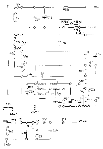
flyback converter providing an isolated supply to LEDs.
[0004] It is desirable to provide various circuit protection features for an
LED driver circuit
utilizing a PFC controller without having to add expensive circuit components
or complexity that
increases the cost of implementing typical circuit protection schemes
disclosed by the prior art.
SUMMARY
[0005] The present invention may comprise one or more of the features recited
in the
attached claims, and/or one or more of the following features and combinations
thereof.
[0006] An illustrative LED driver circuit is based on a transition-mode power
factor
correction controller (PFC) integrated circuit using flyback topology. The LED
driver circuit
, , CA 02798496 2012-11-30
features a universal input circuit having various fault and surge protections,
output circuit open
load and short circuit protection, and main transformer over temperature
protection.
[0007] Additional features of the disclosure will become apparent to those
skilled in the art
upon consideration of the following detailed description of the illustrative
embodiment.
BRIEF DESCRIPTION OF THE DRAWINGS
[0008] The detailed description particularly refers to the accompanying
figures in which:
[0009] Figs. lA and 1B is a schematic diagram of an LED driver circuit
according to the
present invention, Fig. lA illustrating the input circuit and Fig. 2B
illustrating the isolated output
circuit;
[0010] Fig. 2 is a schematic diagram of a power line input and EMI portion of
the LED
driver circuit of Figs. lA and 1B;
[0011] Fig. 3 is an illustrative pin layout diagram of IC U4 of the LED driver
circuit of Figs.
1 A and 1B;
[0012] Fig. 4. is a graph of the illustrative voltage regulation and current
regulation control
curve of IC U4 of Figs. lA and 1B;
[0013] Fig. 5 is a schematic diagram of first embodiment of an output circuit
portion of the
LED driver circuit of Figs. lA and 1B; and
[0014] Fig. 6 is a schematic diagram of a second embodiment of an output
circuit portion
with over temperature protection of the LED driver circuit of Figs. lA and 1B.
DESCRIPTION OF THE ILLUSTRATIVE EMBODIMENTS
2
CA 02798496 2012-11-30
[0015] For the purposes of promoting and understanding the principals of the
invention,
reference will now be made to one or more illustrative embodiments illustrated
in the drawings
and specific language will be used to describe the same.
[0016] LED Driver with Flyback Transformer Overview
[0017] Referring to Figs. 1A and 1B, the schematic for an illustrative
embodiment of a driver
circuit for LED lighting is shown. The PFC input circuit portion of the driver
circuit illustrated
in Fig. 1A is based on a transition-mode PFC controller IC Ul, for example an
L656x series IC,
for example, L6562A, available from STMicroelectronics of Coppell, Texas and
Geneva,
Switzerland. The driver circuit uses a flyback converter topology and
accommodates a power
line input voltage ranging from 120 Vac to 277 Vac.
[0018] Referring to Fig. 1A, a boost converter is connected to the output of
rectifier bridge
diodes Dla, Dlb, Dlc, and Did. A flyback switch includes a MOSFET Q1 and is
driven by the
IC Ul. The boost transformer Ti provides the coupling between a primary
winding Np and a
secondary winding Ns (Fig. 1B). Diode D3 and R32/C32 circuit clamp the peak
leakage
inductance voltage spike at Q1 turn-off.
[0019] Upon startup, IC Ul is powered by circuit voltage supply VCC across
capacitor C6,
which is charged from line rectified DC voltage VDC via resistors R1, R2a, and
R2b.
Transformer Ti's auxiliary winding Na and associated components can be used to
generate 15V
VCC for IC Ul during normal operation.
[0020] Resistor R3 is also connected to auxiliary winding Na to provide a
transformer signal
to the L656x current sensing (ZCD) pin of IC Ul, turning on MOSFET Q1 at every
switching
cycle. Resistor R34 senses the current flowing into the transformer primary
side. Once the signal
at the current sense pin ZCD has reached the level programmed by an internal
multiplier of the
3
CA 02798496 2012-11-30
,
L656x, MOSFET Q1 turns off. A voltage divider formed by resistors R7/R8/R9 and
R5
provides a multiplier (MULT) pin of IC Ul with instantaneous voltage
information which is used
to modulate the current flowing into the transformer Ti primary side. IC U2a/b
is an
optocoupler. The input side U2a is located in the PFC/input circuit portion of
the circuit (Fig.
1A), and the output side U2b is located in the output circuit portion of the
LED driver circuit
(Fig. 1B). Optocoupler U2 transfers a control signal from the output circuit
portion of the LED
driver circuit to the PFC/input circuit portion of the LED driver circuit, for
example, to the INV
pin, inverting input of the error amplifier of the IC Ul, which also doubles
as an ON/OFF control
input.
[0021] Flyback LED Driver Control Circuit Overview
[0022] Referring to Fig. 1B, an output rectifier diode D5 coupled to the
secondary winding
Ns of the boost transformer Ti is a fast recovery type diode. Capacitor C24 is
coupled across the
output to filter out high frequency ripple. The output voltage ripple
frequency is twice the input,
measured as 120HZ. The resulting voltage ripple is less than 3.0% at the LED
lamp and the
current ripple is about 20% through LED lamp.
[0023] The output voltage and current feedback to the PFC, IC Ul is provided
by the
optocoupler U2a/b. The optocoupler input U2b is driven by a control output,
OUT pin 5 of IC
U4 (Fig. 3), a constant voltage, constant current secondary controller
integrated circuit U4, for
example, SEA05 available from STMicroelectronics of Coppell, Texas and Geneva,
Switzerland.
The IC U4 includes a dual control loop to perform current control and voltage
control (CC and
CV) regulation. The IC U4 integrates a voltage reference, two Op Amps, and a
low side current
sensing circuit. The control output, OUT pin 5, is a common open-drain output
of the two
internal op-amps, and Vcc pin 6, is the voltage supply for IC U4.
4
, ,. CA 02798496 2012-11-30
[0024] Output voltage sensing is provided using resistors R21 and R20/R20b,
which form a
voltage divider circuit, the midpoint of which is coupled to IC U4 Vctrl
input, pin 3 for SEA05,
to sense the output voltage available to drive the LED lamp. Vctr is an
inverting input of the
voltage loop op-amp of IC U4. Output current sensing is provided using
resistor network R25,
R25b1, R25b2 coupled to the IC U4 Ictrl input, pin4 for SEA05, for low-side
current sensing.
Isense, pin 1 of IC U4, is an inverting input of the current loop op-amp. GND,
pin 2 of IC U4 is
the ground, return of the bias current of the device and provides a 0 V
references for all voltages.
[0025] Circuit Input Protection Features
[0026] Referring to Fig. 2, a power line input and EMI portion of the LED
driver circuit is
illustrated. The power input circuit includes a fuse Fl, an EMI filter
inductor Li and associated
capacitors, Varistor V1, an inrush limiting device R2, and a rectifier bridge
using diodes Di a,
Dlb, Dlc, and Did.
[0027] The input circuit provides various fault and surge protections. Fuse F
1 is provided in
series with the input power line, and thus prevents shorting of the input
power line by a short
failure within the driver circuit. Varistor V1 is electrically coupled between
the power line input
and the neutral input and protects the circuit from voltage surges. In order
to support a universal
power line input feature, a varistor with a voltage rating of 320 V can be
used.
[0028] Inrush limiting device R2 can be a Negative Temperature Coefficient
(NTC)
thermistor. For example, before power is supplied to the driver circuit, the
temperature of the
NTC thermistor R2 is about room temperature and the NTC thermistor has a high
resistance
value; therefore, the NTC thermistor limits power line current when power is
first supplied and
the driver circuit is starting. After startup, the temperature of NTC
thermistor R2 rises and its
resistance value decreases; therefore, power loss due to the NTC thermistor R2
decreases. NTC
5
, , CA 02798496 2012-11-30
thermistor R2 can thus reduce the power line inrush current when the driver
circuit is first
starting.
[0029] Circuit Output Protection Features
[0030] Referring to Fig 5, illustrating a first illustrative embodiment of
the output portion of
the LED driver circuit, the output voltage and current feedback is provided to
the input of the
optocoupler U2, driven by the OUT pin 5 of IC U4. The voltage regulation
function of IC U4 is
used to limit the output voltage in the event of an open circuit. And the
current regulation
function of the IC U4 is used to provide a constant current to the LED lamps
connected to the
driver circuit. When the equivalent load resistance increases above a certain
value, the current
from the driver circuit to the LED lamps will decrease. Fig. 4 illustrates the
constant current CC
and constant voltage CV control curve for the IC U4 under normal conditions.
[0031] In the event that the LED driver circuit load (output LED+ and LED-)
is an open
circuit, the output voltage can be limited to a predetermined value for
safety. For example, in the
illustrative embodiment shown in Fig. 5, a typical LED lamp is rated for 36 V
and 720 mA. The
junction between resistors R20 and R21 is provided to the Vctrl of IC U4 for
sensing the output
voltage, and thus the output voltage provided by the driver circuit depends on
the voltage divider
circuit comprising resistors R20 and R21. Based on the normal LED lamp rating,
the values of
the resistors R20 and R21 can be selected to provide a maximum output voltage
of 45 Vdc when
the output is an open circuit, and thus no load is provided.
[0032] The output portion of the driver circuit shown in Fig. 5 also
provides a controlled
constant current to the LED lamps. The current sensing resistor R25 is in
series with the
negative output LED- supplied to the LED lamps. In the illustrative
embodiment, the value of
resistor R25 is 0.10 Ohm, 1%. For accurate current sensing of the driver
output, a divider circuit
6
CA 02798496 2012-11-30
having resistors R25b1 and R25b2 coupled in parallel with current sensing
resistor R25, are
selected to provide the desired current output.
[0033] The illustrative IC U4 uses 50mV for current sensing. The sensing
resistor for rated
lamp current of 720mA lamp is thus determined to be 50mV/0.72 A = 69.4 mohm.
Because of
the difficulty in finding such low value and accurate sensing resistor, the
two resistors R25b1 and
R25b2 in parallel with current sensing resistor R25 are selected to provide
the desired resistance
that will provide 50mV at a current flow of 720 mA through resistor R25. For
example, the total
value of resistor R25b1+R25b2 can be about 100 times the value of resistor
R25.
[0034] Output short circuit protection is also provided by IC U4. There are
two different
times relating to the driver circuit when the LED load could be shorted: the
output is shorted
before the driver circuit has started, and the output is shorted after the
driver circuit has started.
While the resistor R100, 15 ohms, provides some protection to the IC U4, more
short circuit
protections are desired.
[0035] In the event the load on the driver circuit output (LED+ and LED-) is
shorted before
the LED driver circuit has started, in the output circuit of Fig. 5 there
would be no power being
supplied to the IC U4 Vcc pin for it to properly work. To resolve this issue,
an additional or
alternative source of power can be provided to the IC U4 Vcc pin, as is
illustrated in the lower
portion of Fig. 1B. Specifically, transformer output Na2 and associated
components provide DC
power to the IC U4 Vcc when power is not otherwise available from the input
circuit shown in
Fig. 1A, so that IC U4 is operational as the input circuit is started, thus
providing output short
circuit protection upon startup of the LED driver circuit.
[0036] In the event the load on the driver circuit output (LED+ and LED-) is
shorted after the
driver circuit has started, rapid discharge of capacitor C12 and a resulting
excessively high
7
, CA 02798496 2012-11-30
current, is a risk. The addition of NTC thermistor R26b, shown in Fig. 5
provides protection
from this risk. For steady state operation after the driver circuit has
started, the electrolytic
output capacitor C12 (1000uF, 50V) is typically charged to about 36 Vdc.
[0037] If an output short develops after the driver circuit has started
normally, the total
normal circuit resistance receiving the charge from capacitor C12 is about 0.2
ohms, therefore,
the initial short-circuit current can be about 180 A. This excessively high
current value can cause
arcing. Adding an NTC thermistor R26b in series with the output LED+
substantially reduces
the arcing current. For example, with a 1 ohm NTC thermistor R26b, the initial
short-circuit
current is reduced to 36 V / 1.2 ohm = 30 A, about 17% of the original value.
For normal driver
circuit operation, after circuit startup and continuing operation, the
temperature of NTC
thermistor R26b increases, and the power loss due to thermistor R26b is
substantially reduced.
[0038] Fig. 6 is a schematic of a second illustrative output circuit that
incorporates over
temperature protection (OTP), facilitated by components responsive to
increases in the
temperature of transformer Ti. The voltage divider resistors R21, R20, and
resistors R20a and
R20b and PTC thermistors R4 and R4b provide the OTP function. Without the
thermistors
providing OTP, the output circuit is equivalent to a short across resistor
R20b. As discussed
above, resistors R20 and R21 provide a voltage feedback divider and are
selected to provide a
maximum output voltage of 45 Vdc.
[0039] Thermistors R4 and R4b can be thermally coupled with the transformer
Ti. In the
event of an over-temperature situation, as the temperature of transformer Ti
rises, the resistance
value across thermistors R4 and R4b increases. At normal (room) operating
temperature, the
resistance of thermistors R4 and R4b are within the range of several hundred
ohms, or less. As
8
= CA 02798496 2012-11-30
the thermistor temperatures increase, the resistance of thermistors R4 and R4b
can rise to be
several hundred kilo-ohms.
[0040] Assuming resistor R20a = 0 ohm, and resistor R20b is open, PTC
thermistors R4 and
R4b provide a current divider circuit at low temperatures and the resistance
of PTC thermistors
R4 and R4b is low enough at low temperatures to not affect the divider
circuit. At this
low/normal temperature condition, voltage output for the circuit is thus
limited to 45Vdc;
however, as the temperatures rise and reach a certain level, the resistance of
R20+R4 increases,
causing a decrease in the LED output voltage, and therefore, the current and
power output also
decreases. With the output power to the LED lamps decreasing, both the LED
lamps and the
driver circuit should experience a reduction of temperature.
[0041] For example, thermistor R4 can be a through-hole type and be mounted
near the main
transformer Ti, and thermistor R4b can be an SMD type and be mounted on the
PCB under the
main transformer Ti. Thermistors R4 and R4b provide redundancy in the driver
circuit to avoid
a possible failure mode.
[0042] Advantageously, because the thermistors R4 and R4b can be discrete
values, the
resistance of the resistor net (R20, R20a, R20b, R4 and R4b) will provide an
advantage of a
smaller variance from unit to unit for thermal performance at mass production.
[0043] While the invention has been illustrated and described in detail in the
foregoing
drawings and description, the same is to be considered as illustrative and not
restrictive in
character, it being understood that only illustrative embodiments thereof have
been shown and
described and that all equivalents and all changes and modifications known in
the art that come
within the spirit and scope of the invention as defined herein are desired to
be protected.
9