Note : Les descriptions sont présentées dans la langue officielle dans laquelle elles ont été soumises.
CA 02798891 2014-11-28
DC PASS RF PROTECTOR
HAVING A SURGE SUPPRESSION MODULE
BACKGROUND
[0002] 1. Field
[0003] The present invention generally relates to surge protectors and
improvements
thereof. More particularly, the present invention relates to RF protectors
having surge
suppression modules and improvements thereof.
[0004] 2. Description of the Related Art
[00051 Communications equipment, computers, home stereo amplifiers,
televisions and
other electronic devices are increasingly manufactured using small electronic
components
that are vulnerable to damage from electrical energy surges. Surge variations
in power and
transmission line voltages, as well as noise, can change the operating
frequency range of
connected equipment and severely damage or destroy electronic devices.
Electronic devices
impacted by these surge conditions can be very expensive to repair or replace.
Therefore, a
cost effective way to protect these devices and components from power surges
is needed.
[0006] Harmful electrical energy surges can originate from a variety of
possible causes.
One such cause is radio frequency (RF) interference that can couple to power
or transmission
lines from a multitude of sources. The power or transmission lines act as
large antennas that
may extend over several miles, thereby collecting a significant amount of RF
noise from such
sources as radio broadcast antennas. Another source of RF interference stems
from
equipment connected to the power or transmission lines that conducts along
those lines to the
1
CA 02798891 2014-11-28
equipment to be protected. A further cause of harmful electrical energy surges
is lightning
and typically arises when a lightning bolt strikes a component or transmission
line that is
coupled to the protected hardware or equipment. Lightning surges generally
include DC
electrical energy and AC electrical energy up to approximately I MHz in
frequency and are
complex electromagnetic energy sources having potentials estimated from 5
million to 20
million volts and currents reaching thousands of amperes.
[0007] Surge protectors protect electronic equipment from damage due to the
large
variations in the current and voltage resulting from lightning strikes,
switching surges,
transients, noise, incorrect connections or other abnormal conditions or
malfunctions that
travel across power or transmission lines. Ideally, an RF surge suppression
device would
have a compact size, a low insertion loss and a low voltage standing wave
ratio (VSWR) that
is capable of protecting hardware equipment from harmful electrical energy
emitted from the
above described sources.
SUMMARY
100081 An apparatus for protecting hardware devices from surges is
disclosed. In one
embodiment, a DC pass RF surge protector may include a housing defining a
cavity, a first
and a second conductor positioned within the cavity of the housing, a
capacitor positioned
within the cavity and electrically connected between the first and the second
conductor, a first
spiral inductor positioned within the cavity of the housing and having a first
terminal coupled
to the first conductor and a non-linear protection device positioned outside
the cavity of the
housing and electrically connected to a second terminal of the first spiral
inductor.
[0009] In another embodiment, a DC pass RF surge suppressor may include a
first
housing defining a first cavity having a central axis, input and output
conductors disposed in
the first cavity of the first housing and positioned substantially along the
central axis, a
capacitor connected in series with the input conductor and the output
conductor, a first spiral
2
CA 02798891 2014-11-28
inductor having a first terminal connected to the input conductor and a second
terminal and a
second spiral inductor having a first terminal connected to the output
conductor and a second
terminal. The DC pass RF surge suppressor further includes a second housing
defining a
second cavity and connected to the first housing, at least one feed-through
for connecting the
first cavity to the second cavity, a first surge protection element disposed
in the second cavity
of the second housing and connected to the second terminal of the first spiral
inductor
through the at least one feed-through and a second surge protection element
disposed in the
second cavity of the second housing and connected to the second terminal of
the second
spiral inductor through the at least one feed-through.
[0010] In still another embodiment, a DC pick-off and RF pass-through surge
protector
may include a housing defining a first cavity having a central axis and a
second cavity in
communication with the first cavity via a passageway, input and output
conductors disposed
in the first cavity of the housing and extending substantially along the
central axis, a capacitor
disposed in the first cavity and connected in-line between with the input
conductor and the
output conductor, a first spiral inductor disposed in the first cavity and
having an inner radius
connected to the input conductor and an outer radius and a second spiral
inductor disposed in
the first cavity and having an inner radius connected to the output conductor
and an outer
radius connected to the housing. The DC pick-off and RF pass-through surge
protector
further includes a surge protection device disposed in the second cavity of
the housing and
electrically connected to the outer radius of the first spiral inductor via
the passageway.
BRIEF DESCRIPTION OF THE DRAWINGS
[0011] Other systems, methods, features, and advantages of the present
invention will be
or will become apparent to one with skill in the art upon examination of the
following figures
and detailed description. It is intended that all such additional systems,
methods, features,
and advantages be included within this description, be within the scope of the
present
0
CA 02798891 2012-11-07
WO 2011/143320
PCTMS2011/036087
Invention, and be protected by the accompanying claims. Component parts shown
in the
drawings are not necessarily to scale, and may be exaggerated to better
illustrate the
important features of the present invention. In the drawings, like reference
numerals
designate like parts throughout the different views, wherein:
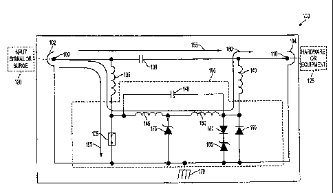
[0012] FIG. I is a schematic circuit diagram of a DC pass RF coaxial surge
protector with
a gas tube in accordance with an embodiment of the invention;
[0013] FIG. 2 is a cross-sectional view of the DC pass RF coaxial surge
protector having
the schematic circuit diagram shown in FIG. 1 in accordance with an embodiment
of the
invention;
100141 FIG. 3 is a schematic circuit diagram of a DC injector/pick-off and
RF pass-
through coaxial surge protector with a gas tube in accordance with an
embodiment of the
Invention; and
[0015] FIG. 4 is a cross-sectional view of the DC injector/pick-off and RF
pass-through
coaxial surge protector having the schematic circuit diagram shown in FIG. 3
in accordance
with an embodiment of the invention.
DETAILED DESCRIPTION
100161 Referring now to FIG. 1, a schematic circuit diagram of a DC pass RF
coaxial
surge protector 100 is shown. The surge protector 100 protects hardware or
equipment 125
connected to the surge protector 100 from an electrical surge 120 that could
damage or
destroy the hardware or equipment 125. The surge protector 100 includes a
number of
different electrical components, such as capacitors, inductors and diodes. For
illustrative
purposes, the schematic circuit diagram of the surge protector 100 will be
described with
reference to specific capacitor, inductor or diode values to achieve specific
surge protection
capabilities. However, other specific capacitor, inductor or diode values or
configurations
may be used to achieve other electrical or surge protection characteristics.
Similarly,
4
CA 02798891 2012-11-07
WO 2011/143320
PCTTUS2011/036087
although the preferred embodiment is shown with particular capacitive devices,
spiral
inductors and gas tube suppression elements, it is not required that the exact
elements
described above be used in the present invention. Thus, the capacitive
devices, spiral
inductors and gas tubes are to illustrate various embodiments and not to limit
the present
invention.
[0017) The frequency range of operation for the surge protector 100
described by the
schematic circuit diagram is between about 680 MHz and about 2.5 GlEIz. In one
embodiment, the frequency range of operation is 680 MHz to 1.0 GHz, within
which the
insertion loss is specified less than 0.1 dB and the voltage standing wave
ratio (VSWR) is
specified less than 1.1:1. In another embodiment, the frequency range of
operation is 1.0
MHz to 3.0 MHz (a telemetry band), within which the insertion loss is
specified less than 0.4
dB and the VSWR is specified less than 1.4:1. The values produced above can
vary
depending on the frequency range, degree of surge protection and RF
performance desired.
100181 The surge protector 100 has two connection terminals including an
input port 102
having an input center conductor 109 and an output port 104 having an output
center
conductor 110. The connection at the input port 102 and the output port 104
may be a center
conductor such as a coaxial line with center pins as the input center
conductor 109 and the
output center conductor 110 for propagating DC currents and RF signals and an
outer shield
that surrounds the center pins. Moreover, the input port 102 may function as
an output port
and the output port 104 may function as an input port. By electrically
connecting the surge
protector 100 along a conductive path or transmission line between an input
signal or power
source and the connecting hardware or equipment 125, an electrical surge 120
present at the
input port 102 that could otherwise damage or destroy the hardware or
equipment 125 will
instead dissipate through the surge protector 100 to ground, as discussed in
greater detail
herein. The protected hardware or equipment 125 can be any communications
equipment,
CA 02798891 2012-11-07
WO 2011/143320
PCT/US2011/036087
cell tower, base station, PC computer, server, network component or equipment,
network
connector or any other type of surge sensitive electronic equipment.
100191 The surge protector 100 has various components coupled between the
input center
conductor 109 and the output center conductor 110, the components structured
to form a
desired impedance (e.g., 50 a) and for providing various signal paths through
the surge
protector 100. These signal paths include an RF path 155, a DC path 160 and a
main surge
path 165. The RF path 155 includes the input center conductor 109, a DC
blocking capacitor
130 and the output center conductor 110. During normal operations, RF signals
travel across
the RF path 155 to the hardware or equipment 125. The protected hardware or
equipment
125 can receive or transmit RF signals along the RF path 155, thus the surge
protector 100
can operate in a bidirectional RF manner. In the preferred embodiment, better
surge
performance is exhibited when operating in a unidirectional manner from the
input port 102
to the output port 104.
10020] The capacitor 130 is placed in series with the input center
conductor 109 and the
output center conductor 110 in order to block DC signals and undesirable surge
transients.
The capacitor 130 has a value between about 3 picoFarads (pF) and about 15 pF
wherein
higher capacitance values .allow for better low frequency performance.
Preferably, the
capacitor 130 has a value of about 4.5 pF. The capacitor 130 is a capacitive
device realized
in either lumped or distributed form. Alternatively, the capacitor 130 can be
realized by
parallel rods, coupling devices, conductive plates or any other device or
combination of
elements which produce a capacitive effect. The capacitance of the capacitor
130 can vary
depending upon the frequency of operation desired and the capacitor 130 will
block the flow
of DC signals while permitting the flow of AC signals depending on this chosen
capacitance
and frequency. At certain frequencies, the capacitor 130 may. operate to
attenuate the AC
signal.
6
CA 02798891 2012-11-07
WO 2011/143320
PCT/US2011/036087
[0021] Although DC
signals are thus prevented from traveling along the RF path 155,
they can still be supplied through the surge protector 100 to the connecting
hardware or
equipment 125 via the DC path 160. The DC path 160 includes the input center
conductor
109, a first spiral coil or inductor 135, a second spiral coil or inductor
140, intermediate coils
or inductors 145 and 150 and the output center conductor 110. A DC signal on
the input
center conductor 109 travels outside of the RF path 155 and around the
blocking capacitor
130 by propagating along the first spiral inductor 135, along the intermediate
inductors 145
and 150 and along the second spiral inductor 140 where the DC signal travels
to the output
center conductor 110.
[0022] The main surge
path 165 provides a path for the surge 120 to travel and dissipate
to ground instead of propagating through to the connected hardware or
equipment 125.
Several electrical components 195 are additionally coupled between the input
center
conductor 109 and the output center conductor 110 for helping to mitigate the
electrical surge
120 that may be present at the input port 102 of the surge protector 100. The
electrical
components 195 are mounted or integrated with a printed circuit board or a
common ground
base plate, the printed circuit board or base plate positioned within the
surge protector 100 as
described in greater detail in FIG. 2. The electrical components 195 include a
gas tube 105,
the intermediate inductors 145 and 150, a capacitor 148, zener diodes 175 and
185 and diodes
180 and 190. The gas tube 105 and the diode components (175, 185, 180 and 190)
are
coupled between a common ground 170 (e.g., a housing of the surge protector
100) and a
node at some location along the DC path 160.
[0023] During a surge
condition, the surge 120 is blocked by the blocking capacitor 130
and is routed through the first spiral inductor 135. The surge 120 flows along
the main surge
path 165 from the input center conductor 109, along the first spiral inductor
135 and across
the gas tube 105. Auxiliary surge paths exist through the diode components
(175, 185, 180
7
CA 02798891 2012-11-07
WO 2011/143320
PCT/US2011/036087
and 190) to the ground 170 (e.g., a housing of the surge protector 100), as
discussed in
greater detail herein.
[0024] The gas tube 105
contains hermetically sealed electrodes that ionize gas during
use. When the gas is ionized, the gas tube 105 becomes conductive and the
breakdown
voltage is lowered. The breakdown voltage varies and is dependent upon the
rise time of the
surge 120. Therefore, depending on the characteristics of the surge 120,
several
microseconds may elapse before the gas tube 105 becomes ionized and hence
conductive.
Thus, the leading portion of the surge 120 passes to the intermediate
inductors 145 and 150
instead of passing through the gas tube 105. The capacitor 148 connected in
parallel across
the intermediate inductors 145 and 150 is used as a low frequency bypass
capacitor for the
tuning of telemetry signals.
[0025] At low
frequencies (e.g., DC signals), the intermediate inductors 145 and 150 act
as shorts and allows voltages and/or currents to flow unimpeded to the other
components. At
higher voltage wavefronts and di/dt levels, such as during surge conditions,
the inductors 145
and 150 will impede currents and develop a voltage drop, effectively enabling
auxiliary surge
paths to the ground 170 through the diode components at varying turn-on
voltages and turn-
on times and delaying the surge currents to allow the gas tube 105 time to
trigger. When a
leading edge of the surge 120 propagates through to the intermediate inductors
145 and 150,
one or more of the diodes (e.g., the zener diodes 175 and 185 and the diodes
180 and 190)
divert the portion of the surge 120 to the ground 170 rather than allowing the
surge 120 to
propagate to the output center conductor 110. These auxiliary surge paths
operate to
dissipate the surge 120 until the gas tube 105 becomes conductive and allows
the surge 120 to
flow to the ground 170 via the main surge path 165.
[00261 The zener diodes
175 and 185 and the diodes 180 and 190 have faster turn-on
times and lower turn-on voltages compared to the gas tube 105. The diode
components 180,
8
CA 02798891 2012-11-07
WO 2011/143320
PCT/US2011/036087
185 and 190 are configured for a specific turn-on voltage (e.g., 40 volts) and
will conduct to
the ground 170 first. Secondly, the zener diode 175 is configured to have a
higher turn-on
voltage (e.g., 80-90 volts) than the diode components 180, 185 and 190 and
will conduct to
the ground 170 at some point in time afterwards. Lastly, the gas tube 105 is
configured to
have an even higher turn-on voltage (e.g., 300 volts) and will conduct to the
ground 170 last.
[0027) In an alternative embodiment, the gas tube 105 or the diode
components (175,
180, 185 or 190) may be replaced or supplemented with a different non-linear
element or
surge protection element or device for dissipating the surge 120 to the ground
170 along the
main surge path 165. For example, a metal oxide varistor (MOV), diode or any
combination
thereof may be incorporated. If the voltage at the MOV is below its clamping
or switching
voltage, the MOV exhibits a high resistance. If the voltage at the MOV is
above its clamping
or switching voltage, the MOV exhibits a low resistance. Hence, MOVs can
effectively
provide surge protection and are sometimes referred to as non-linear resistors
due to their
nonlinear current-voltage relationship.
[00281 The gas tube 105 is coupled at a first end to the first inductor 135
and at a second
end to the common ground 170. The gas tube 105 has a capacitance value of
about 2 pF and
a turn-on voltage of between about 90 volts and about 360 volts. The selection
of the turn-on
voltage for the gas tube 105 is a function of the RF power of the surge
protector 100. For
example, a turn-on voltage of 360 volts will result in an RF power handling
capacity of about
5,000 watts. Moreover, the high RF impedance provided by the first and second
spiral
inductors 135 and 140 allow for higher RF power to travel in the RF path 155
without turning
on the gas tube 105. Hence, changing the gas tube 105 to have a different turn-
on voltage
affects the RF power limitations but does not affect the RF frequency range or
tuning of the
surge protector 100.
9
CA 02798891 2012-11-07
WO 2011/143320
PCT/US2011/036087
[0029] The gas tube 105
is isolated from (i.e. is not directly connected to) the input center
conductor 109 by the first spiral inductor 135. Similarly, the gas tube 105 is
isolated from the
output center conductor 110 by the second spiral inductor 140 and the
intermediate inductors
145 and 150. The first and second spiral inductors 135 and 140 provide RF
isolation from the
gas tube 105 and other components that are known to create passive inter-
modulation (PIM).
The incorporation of an RF high impedance element (e.g., an inductor, a
quarter-wave stub,
etc) between the RF path 155 and the gas tube 105 significantly reduces the
amount of PIM
in the RF path 155. That is, the first and second spiral inductors 135 and 140
prevent the gas
tube 105 and other surge mitigation components from being directly connected
to the RF path
155. The first and second spiral inductors 135 and 140 may thus be replaced
with quarter-
wave stubs or other RF high impedance elements to achieve a similar purpose.
[0030) Turning now to
FIG. 2, a cross-sectional view of the DC pass RF coaxial surge
protector 100 having the schematic circuit diagram of in FIG. I is shown. The
surge
protector 100 has a first housing 205 that defines a first cavity 210. The
first cavity 210 is
preferably formed in the shape of a cylinder and has an inner radius of
approximately 432.5
mils. In an alternative embodiment, the first cavity 210 can be formed in any
shape and of
varying sizes. The input center conductor 109 and the output center conductor
110 are
positioned concentric with and located within the first cavity 210 of the
first 'housing 205.
The surge protector 100 has a second housing 215 that extends from the first
housing 205.
The first housing 205 and the second housing 215 may be formed as a single
housing. The
second housing 215 defines a second cavity 220 for housing the electrical
components 195
(see FIG. 1).
[0031) The input center
conductor 109, the first spiral inductor 135, the capacitor 130, the
second spiral inductor 140 and the output center conductor 110 are positioned
within the first
cavity 210 of the first housing 205. The input and output center conductors
109 and 110 are
CA 02798891 2012-11-07
WO 2011/143320
PCTTUS2011/036087
positioned along a central axis within this first cavity 210. The first
inductor 135 is
positioned along a first plane and the second inductor 140 is positioned along
a second plane,
the first plane being positioned substantially parallel to the second plane.
In one
embodiment, the central axis of the input and output center conductors 109 and
110 is
positioned substantially perpendicular to the first plane and the second
plane.
[00321 The first and second spiral inductors 135 and 140 have small foot
print designs
and may be formed with flat or planar geometries. The first and second spiral
inductors 135
and 140 have values of between about 10 nanoHenries (nH) and about 25 nH with
a preferred
range of about 17 to 20 nH, as measured at around 100 MHz. The chosen values
for the first
and second spiral inductors 135 and 140 help determine the specific RF
frequency ranges of
operation for the surge protector 100. The diameter, surface. area, thickness
and shape of the
first and second spiral inductors 135 and 140 can be varied to adjust the
operating frequencies
and current handling capabilities of the surge protector 100. In one
embodiment, an iterative
process may be used to determine the diameter, surface area, thickness and
shape of the first
and second spiral inductors 135 and 140 to meet the requirements of a
particular application.
In the preferred embodiment, the diameter of the first and second spiral
inductors 135 and
140 of the surge protector 100 is about 0.865 inches and the thickness of the
first and second
spiral inductors 135 and 140 is about 0.062 inches. Furthermore, the spiral
inductors 135 and
140 spiral in an outward direction.
[0033] The material composition of the first and second spiral inductors
135 and 140
helps determine the amount of charge that can be safely dissipated across the
first and second
spiral inductors 135 and 140. A high tensile strength material allows the
first and second
spiral inductors 135 and 140 to discharge or divert a greater amount of
current. In one
embodiment, the first and second spiral inductors 135 and 140 are made of a
7075-T6
Aluminum material. Alternatively, any material having sufficient tensile
strength and
11
CA 02798891 2014-11-28
conductivity for a given application may be used to manufacture the first and
second spiral
inductors 135 and 140. Each of the components or the housing may be plated
with a silver
material or a tri-metal flash plating. This reduces or eliminates the number
of dissimilar or
different types of metal connections or components in the RE path to improve
PIM
performance.
[0034] The first and second spiral inductors 135 and 140 are positioned
within the first
cavity 210. Each of the first and second spiral inductors 135 and 140 has a
first terminal with
an inner radius of approximately 62.5 mils and a second terminal with an outer
radius of
approximately 432.5 mils. The first terminal of the first spiral inductor 135
is coupled to the
input center conductor 109 and the first terminal of the second spiral
inductor 140 is coupled
to the output center conductor 110. The second terminal of the first spiral
inductor 135 is
coupled to the gas tube 105. Similarly, the second terminal of the second
spiral inductor 140
is coupled to the gas tube 105 through various electrical components 195. The
first housing
205 may operate as a common ground connection to facilitate an easily
accessible grounding
location for the various surge mitigation elements (e.g., 105, 175, 185 and
190).
[0035] Each spiral of the first and second spiral inductors 135 and 140
spirals in an
outward direction. In one embodiment, each of the first and second spiral
inductors 135 and
140 has three spirals. The number of spirals and thickness of each spiral can
be varied
depending on the requirements of a particular application. The spirals of the
first and second
spiral inductors 135 and 140 may be of a particular known type such as the
Archimedes,
Logarithmic, Hyperbolic or any combination of these or other spiral types.
[0036] During a surge condition, the surge 120 (see FIG. 1) first reaches
the first terminal
of the first spiral inductor 135. The surge 120 then travels through the
spirals of the first
spiral inductor 135 in an outward direction from the first terminal to the
second terminal.
Once the surge 120 reaches the second terminal, the surge 120 is dissipated to
ground through
one or more of the following elements: the gas tube 105, the zener diodes 175
and 185,
12
CA 02798891 2014-11-28
and/or the diodes 180 and 190 (see FIG. 1). The main portion of the surge 120
is passed
across the gas tube 105 (see FIG. 1) while auxiliary portions of the surge 120
that are not
diverted by the gas tube 105 are diverted to ground by the zener diodes 175
and 185 and/or
the diodes 180 and 190.
[0037] With reference to FIG. 1, the electrical components 195 are mounted
or integrated
with a printed circuit board or a common ground base plate that is positioned
within the
second cavity 220 of the second housing 215 and attached to the first housing
205 or the
second housing 215 with screws or other fasteners. The electrical components
195 are thus
positioned within the second cavity 220 of the second housing 215 and
therefore isolated
from the components along the RF path 155, which are positioned within the
first cavity 210
of the first housing 205. DC signals are moved out of the first cavity 210 and
into the second
cavity 220 via the first spiral inductor 135. Similarly, DC signals are moved
back into the
first cavity 210 from the second cavity 220 via the second spiral inductor
140. In an
alternative embodiment, the second cavity 220 or second housing 215 may not be
needed and
the DC path 160 or the main surge path 165 can rather be routed to any
location outside of
the first cavity 210 of the first housing 205 in order to isolate them from
the RF path 155
traveling within the first cavity 210.
[0038] In the preferred embodiment, one or more feed-throughs or
passageways 225 are
used to electrically connect elements or components in the first cavity 210
with elements or
components within the second cavity 220. The feed-throughs or passageways 225
allow
electrical wires or other conductive elements to pass signals from the first
cavity 210 to the
second cavity 220 and vice versa. For example, a first electrical wire passes
through one
feed-through or passageway 225 to connect the second terminal of the first
spiral inductor
135 to the gas tube 105 and a second electrical wire passes through a
different feed-through
or passageway 225 to connect the second terminal of the second spiral inductor
140 to the
intermediate inductor 150, the diodes 180 or 190 or the capacitor 148. In an
alternative
13
CA 02798891 2014-11-28
embodiment, more or fewer feed-throughs or passageways 225 may be used. Such a
configuration allows RF signals to travel along the RF path 155 in the first
cavity 210 free
from interference due to the surge mitigation circuitry located in the second
cavity 220.
[0039] Turning now to FIG. 3, a schematic circuit diagram of a DC
injector/pick-off and
RF pass-through coaxial surge protector 300 is shown. The surge protector 300
operates to
protect the hardware or equipment 125 from electrical surges in a similar
fashion to the surge
protector 100 described for FIG. 1 and includes an input port 302 having an
input center
conductor 309 and an output port 304 having an output center conductor 310.
The
connection at the input port 302 and the output port 304 may be a center
conductor such as a
coaxial line with center pins as the input center conductor 309 and the output
center
conductor 310 for propagating DC currents and RF signals and an outer shield
that surrounds
the center pins. The surge protector 300 utilizes many of the same electrical
components as
the surge protector 100, including the blocking capacitor 130, the first and
second spiral
inductors 135 and 140, the gas tube 105, the intermediate inductors 145 and
150, the
capacitor 148, the zener diodes 175 and 185 and the diodes 180 and 190.
Certain components
are electrically connected in a different manner to create signal paths that
differ from those of
the surge protector 100 described in FIG. 1, as discussed in greater detail
herein.
[0040] The surge protector 300 includes an RF path 355 that comprises the
input center
conductor 309, the capacitor 130 and the output center conductor 310. The RF
path 355
operates similar to the RF path 155 described in FIG. 1. The surge protector
300 also
includes a main surge path 365 for enabling the surge 120 present at the input
center
conductor 309 to travel and dissipate to the ground 370 instead of propagating
through the
surge protector 300 and to the connected hardware or equipment 125. The main
surge path
365 is similar to the main surge path 165 described above for FIG. 1.
14
CA 02798891 2012-11-07
WO 2011/143320
PCT/US2011/036087
[0041] The surge protector 300, however, utilizes a different DC path 360
that does not
include the second spiral inductor 140, but rather incorporates an output
inductor 398
connected to the intermediate inductor 150. The DC path 360 thus includes the
input center
conductor 309, the first spiral inductor 135, the intennediate inductors 145
and 150, the
output inductor 398 and a feed-through connector 399. The feed-through
connector 399
enables a DC connection to the hardware or equipment 125. Hence, the DC path
360 is not
coupled back with the RF path 355 for output, but rather remains isolated from
the RF path
355. In addition, the second spiral inductor 140 is not connected to the
intermediate inductor
150, the diodes 180 or 190 or the capacitor 148 as in FIG.1, but rather Is
connected between
the output center conductor 310 and the ground 370. Such a c,oimection enables
DC signals
or surges present at the output center conductor 310 to propagate to the
ground 370 through
the second spiral inductor 140. .
[0042] FIG. 4 is a cross-sectional view of the DC injector/pick-off and RF
pass-through
coaxial surge protector 300 having the schematic circuit diagram shown in FIG.
3. The surge
protector 300 is similar to the surge protector 100 described for FIG. 2 and
incorporates many
of the same electrical components. Thus, many of the sizing, geometry,
orientation, material
or other aspects of the surge protector 100 or its electrical component parts
described above
are applicable to the surge protector 300.
[0043] The surge protector 300 has a first housing 405 that defines a first
cavity 410. The
input center conductor 309 and output center conductor 310 are positioned
concentric with
and located within the first cavity 410 of the first housing 405. The surge
protector 300 has a
second housing 415 that extends from the first housing 405. The first housing
405 and the
" second housing 415 may be formed as a single housing. The second housing
415 defines a .
second cavity 420 for housing the electrical components 395 (see FIG. 3). In
contrast to the
CA 02798891 2014-11-28
surge protector 100 described for FIG. 2, the second housing 415 extends
further outward or
away from the first housing 405.
[0044] The input center conductor 309, the first spiral inductor 135, the
capacitor 130, the
second spiral inductor 140 and the output center conductor 310 are positioned
within the first
cavity 410 of the first housing 405. The input and output center conductors
309 and 310 are
positioned along a central axis within this first cavity 410. The first spiral
inductor 135 is
positioned along a first plane and the second spiral inductor 140 is
positioned along a second
plane, the first plane being substantially parallel to the second plane. The
central axis of the
input and output center conductors 309 and 310 is positioned substantially
perpendicular to
the first plane and the second plane.
[0045] With reference to FIG. 3, the first and second spiral inductors 135
and 140 are
designed, composed or positioned with similar configurations or materials as
described above
for FIG. 2. During a surge condition, the surge 120 first reaches the first
terminal or radius of
the first spiral inductor 135 and travels in an outward direction through the
spirals of the first
spiral inductor 135 to the second terminal or radius of the first spiral
inductor 135. Once the
surge 120 reaches the second terminal or radius of the first spiral inductor
135, the surge 120
is dissipated to ground (e.g., the housing 405) through one or more of the gas
tube 105, the
zener diodes 175 and 185, and/or the diodes 180 and 190.
[0046] The electrical components 395 (see FIG. 3) are mounted or integrated
with a
printed circuit board or a common ground base plate that is positioned within
the second
cavity 420 of the second housing 415 and attached to the first housing 405 or
the second
housing 415 with screws or other fasteners. The electrical components 395 are
therefore
isolated from the components along the RE path 355, which are positioned
within the first
cavity 410. DC signals are moved out of the first cavity 410 and into the
second cavity 420
via the first spiral inductor 135. Like described above for FIG. 2, one or
more feed-throughs
16
CA 02798891 2012-11-07
WO 2011/143320
PCT/US2011/036087
or passageways 425 are utilized for allowing electrical wires or other
conductive elements to
pass signals from the first cavity 410 to the second cavity 420 and vice
versa. While the
surge protector 100 utilizes a plurality of feed-throughs or passageways 225
(see FIG. 2),
only one feed-through 425 is used by the surge protector 300. As stated above
for FIG. 2, no
second housing or second cavity may be needed in an alternative embodiment,
rather the
electrical components 395, the DC path 360 or the main surge path 365 may be
positioned
outside the first cavity 410 of the first housing 405 without being contained
within a second
cavity or a second housing.
[0047] Exemplary embodiments of the invention have been disclosed in an
illustrative
style. Accordingly, the terminology employed throughout should be read in a
non-limiting
manner. Although minor modifications to the teachings herein will occur to
those well
versed in the art, it shall be understood that what is intended to be
circumscribed within the
scope of the patent warranted hereon are all such embodiments that reasonably
fall within the .
scope of the advancement to the art hereby contributed, and that that scope
shall not be
restricted, except in light of the appended claims and their equivalents.
17