Note : Les descriptions sont présentées dans la langue officielle dans laquelle elles ont été soumises.
CA 02801809 2013-01-14
BACKGROUND OF INVENTION
Field of Invention
This invention is to be used for the detection of physical and chemical
changes
regarding, in particular, but not limited to, defects within a structure.
Description of Related Art
The problem this invention aims to remedy is the inability to conveniently
detect
and locate minor material deterioration as a result of water infiltration in a
home.
However, defects in the home also include, but are not limited to, structural
failure of load bearing elements, obscure perforations that can result in
temperature instability or increased heating costs during the winter, as well
as
natural gas leaks. These defects are often detected too late, only after
substantial damage is sustained.
Visual inspection of difficult to access areas, followed by testing with
handheld
instruments is routine when a defect or flaw is suspected. Some instruments
used for leak detection, such as sensitive voltmeters consisting of two
conductive
leads, identify the presence of the flaw by measuring physical properties of
the
materials, such as resistance, and their changes when exposed to moisture.
These handheld devices have a limited area of detection; they require an
experienced operator and methods can become invasive if the location of the
defect has not been precisely determined.
There are preemptive measures used to detect water infiltration, structural
deformation and other physical or chemical effects on materials. Because of
the
need to cover a large area, convenient arrangements of conductors and non-
conductors in a grid-like fashion are used both for detection and ease of
localization.
1
CA 02801809 2013-01-14
Canadian patent application 2689196 is a detector system, which provides
suitable detection of environmental effects. The grid-arranged sensing element
is
constructed with tracks of two separate conductive pathways, printed on an
insulated non-conductive core whose properties change when exposed to a
predetermined effect. The grid arrangement allows for localization of a
change.
US patent 5081422, describes a water detector which uses pairs of laterally
spaced parallel conductors, in two directions normal to one another, arranged
in
a grid fashion. Each pair is sequentially tested and the location of a leak is
pinpointed through association between detection by a pair of conductors in
the
x-direction and another pair in the y-direction.
Canadian patent 2599087 details a leak detection method by apply traversing
conductive wires in a grid fashion and separated from each other by a
nonconductive material at their intersections only, in proximity of an
electrically
conductive surface. There exists a relay whereby each wire is tested
individually
for a leak, which is indicated in the event that current is allowed to pass
through
the electrically conductive surface and through the water into the conductive
wire
in the event of a leak.
Although the aforementioned patents allow localization of defects, their
design
and method of function may restrict their usage to horizontal surfaces or
detecting a single type of defect. Furthermore, regarding water detection in
particular, prior art may require large amounts of water for detection due to
the
poor sensitivity of the detectors. In all cases, the amount of wiring could be
reduced; these include tracks comprised of two conductive elements printed on
a
nonconductive core, parallel spaced pair of conductors and an electrically
conductive surface, which are not wholly required. The same applies to the
number of periphery devices required for implementation. Increasing in the
amount of wiring and connectors to peripheral devices increases the risk for
failure or breaks to occur within the detector system due to a higher number
of
2
CA 02801809 2013-01-14
possible failure points. The invention described here-in addresses the above-
mentioned shortcomings.
SUMMARY OF THE INVENTION
It is a primary object of the present invention to provide a means of
detection of
not only water infiltration, but also a variety of defects within a structure.
It is another object of the invention to provide a means of localization of a
defect
in the event of detection.
It is a further object of the invention to provide a detection method that is
simple
to implement and reliable.
To achieve the aforementioned objectives, a sensor array system has been
designed which is comprised of two pluralities of electrically conductive
elements
separated at their crossing points by one functional constituent of a mosaic
film
interlayer. This will permit the detection of multiple defects mediated by
multiplexing and signal processing circuitry. The configuration of the
networks of
conductive elements not only allows detection but localization of a defect.
The mosaic interlayer contains many constituents. Each constituent may differ
from another and its electrical properties change when subject to a
predetermined condition to allow the detection thereof. Multiple physical and
chemical effects outside the realm of leak detection are possible with such a
detector and are all included as preferred embodiments in this present
invention.
The mosaic film interlayer, in a typical embodiment, is supported upon a thin
non-
conductive grid substructure with continually spaced and ideally square
perforations forming a series of rows and columns. Each perforation contains
protrusions to allow housing of one constituent of the interlayer. Different
3
CA 02801809 2013-01-14
constituents arranged as repeating modules over the entirety of the interlayer
allow for multiple physical and chemical effects to be probed across an area
of
varying size.
Regarding the configuration of the networks of conductive elements of a
typical
embodiment, the invention comprises of one plurality of non-intersecting
conductors travelling longitudinally on one side of the interlayer and a
second
plurality of non-intersecting conductors travelling in preferably a direction
orthogonal to the first on the opposite face of the interlayer. This
configuration
forms a grid of conductive elements where intersections between an element of
the first network and elements in the second network contain a functional
constituent of the interlayer. Unlike prior art, because the network elements
are
brought into proximity as a thin interlayer only separates them, large amounts
of
water are not required for detection of a leak and the detector still
functions when
deployed in any orientation.
The wiring and interrogation of the detector involves pulse signaling coupled
with
time-division multiplexing (TDM), which probes one element of the first
network
and another element from the second network at predetermined times. One end
of each element from one plurality of elements is affixed to a signal-
generating
device and one end of each element from the second network is affixed to a
signal-receiving device. Due to the arrangement of elements as discussed
previously, the position along one axis and the position along the
perpendicular
axis allows for localization of the predetermined effect. The use of pulse
signaling
is adaptive to monitoring changes in electrical properties of the constituents
of
the interlayer and the coupling with TDM reduces the amount of wiring and
periphery devices required for the sensors. The aforementioned design allows
easier installation, even in areas of limited space, and reduces the number of
failure points within the system that would otherwise cause areas to lack
detection.
4
CA 02801809 2013-01-14
Using water infiltration as an example of a predetermined effect to be
detected,
one constituent of the mosaic interlayer could be comprised of a non-
conductive
material that when soaked in water becomes conductive. For instance, the
constituent could comprise of a water-absorbent film impregnated with salt. If
one
element from the first network and another element from the second network are
probed by the signal-processing device and at their intersection is this
particular
constituent of the interlayer, in the event of water infiltration, the
constituent
becomes wet and changes the characteristics of the pulses being transmitted
across the elements. These changes allow processing and interpretation thereof
by the signal-processing device as means of detection of the leak. Transmitted
signals in the form of pulses will change depending on the electrical
properties of
the constituents that make up the interlayer. These electric properties
include
impedance, resistance, capacitance and inductance; for many materials these
characteristics change selectively to a predetermined physical or chemical
condition allowing further applications of detection besides leak detection.
The following example illustrates the above-mentioned extension of
application. If
a constituent of the interlayer contains a piezoresistive material, instead of
a salt-
impregnated sheet, whose electrical resistance changes significantly upon
changes in pressure, physical stress such as snow atop of a roof could be
monitored. Physical strain that would cause deformation of the invention will
result in a change in the electrical properties of the particular constituent,
resulting in a change in the transmission of a signal between elements that
intersect at the constituent to be realized.
If another constituent were a thin-filmed semiconductor, such as a metal
oxide,
whose electrical properties change significantly upon adsorption of a gas,
transmission of the pulse will change allowing for embodiments of the
invention
to also act as a detector of gases such as propane, naphtha or natural gas.
CA 02801809 2013-01-14
Using different constituents of the mosaic interlayer arranged systematically
as
modules across the sensor array in repeated fashion, as demonstrated, may
allow for detection and localization of many predetermined effects
simultaneously
across an area of predetermined size.
DESCRIPTION OF DRAWINGS
In order to visualize the aforementioned and the way objects of the invention
are
fulfilled, an in-depth description of a specific embodiment will be rendered
with
reference to illustrations thereof in the appended figures. These drawings
illustrate only a typical embodiment and are not therefore considered limiting
of
its scope. The present invention will be described with greater detail through
the
use of the accompanying drawings wherein:
Figure 1 displays a top view of the non-conductive grid substructure in the
preferred embodiment.
Figure 2 displays a bottom view of the non-conductive grid substructure shown
in
Figure
1.
Figure 3 displays a top view of the grid substructure with the mosaic
interlayer
installed.
Figure 4 displays a bottom view of the grid substructure with the mosaic
interlayer installed.
Figure 5 shows an isometric view of a singular empty unit of the grid
substructure
that houses a singular constituent of the interlayer.
6
CA 02801809 2013-01-14
Figure 6 shows an isometric view of a singular unit of the sensor containing
portions of the grid substructure installed with a constituent of the mosaic
interlayer and portions of a conductive element from each network.
Figure 7 shows a cross section of the unit in Figure 6 along the centerline
defined
by the lower wire in Figure 6.
Figure 8 displays top views of both pluralities of conductive elements of the
preferred embodiment along with their associated signal-processing devices.
Figure 9 displays an isometric view of the final assembly of the two networks
of
Figure 8 and the interlayer and its substructure from Figure 4.
Figure 10 displays a schematic diagram of the grid of electrical conductors
containing a leak that describes the means of interrogation of a predetermined
physical or chemical effect.
Figure 11 displays a schematic representation of the pulse signaling and TDM
used to interrogate the sensor array.
DESCRIPTION OF THE INVENTION
A sensor array system for detecting and localizing multiple predetermined
effects
as a result of, in particular, but not limited to, defects within a structure.
The
system comprises two pluralities or networks of conductive elements. The
conductive elements in both networks are electrically separated and run in one
direction with one end only of each element affixed to a signal-processing
device.
The two networks are arranged such that elements are ideally orthogonal to one
another and separated by a mosaic interlayer of several varying constituents.
The interlayer typically has the form of a thin film supported upon a non-
conductive grid substructure. A functional constituent of the interlayer is
7
CA 02801809 2013-01-14
sandwiched at the intersection between an element from one network and
elements from the second. These constituents of the interlayer have electric
properties that are altered when subject to a predetermined effect which
allows
detection by probing elements with the signal processing devices to which the
elements are affixed to, in particular, possessing pulse signaling and TDM
capabilities. The sensor array is meant to, but not limited to, cover or be
adhered
to a surface, placed in between layers of construction or embedded within a
structure. The sizing of the sensor array can be accommodated for small or
large
areas of detection dependent upon sizing and spacing of the components of the
device.
Preferred embodiments of the invention as discussed will be described in
detail,
by means of reference to relevant accompanying drawings, where in Figure 1,
the top view of an empty thin grid substructure (1) without the functional
interlayer that it facilitates the support thereof is shown. In typical
embodiments
this grid substructure could be composed of an artificial elastomer or
synthetic
rubber, without exception a polymer that is relatively non-conductive in
nature.
This would allow flexibility of the sensor array to accommodate surfaces of
irregular geometries. The grid substructure will also serve as mechanical
support
for a structure in which the sensor array is embedded, if the substructure is
made
of a more durable material. The substructure contains a series of continuously
spaced square perforations (2) forming a grid of columns and rows that contain
protrusions from all faces of the perforation that enable support of the
functional
interlayer for which more detail is provided in Figure 5. Indents (3) are a
guide to
the placement of the conductive elements from one network where elements run
in one direction. The size of the perforations dictates the resolution for
detection.
In the case of small sized perforations arranged continuously, greater
resolution
of detection and localization will be achieved. Although the typical
embodiment
contains only a single continuous substructure, alternative embodiments can
use
multiple interspersed smaller grid substructure units to accommodate different
geometries or to selectively probe specific areas.
8
CA 02801809 2013-01-14
Regarding Figure 2, the bottom view of the empty, thin grid substructure shows
indents (5) that act as a guide for placement of conductive elements from the
second network that traverse elements from the first network. As illustrated,
conductive elements of the second network cross elements from the first
network
over the perforations (2).
A filled grid substructure (10) with the multi-functional mosaic interlayer
installed
is shown in Figure 3. The bottom view of the filled grid substructure (15) is
shown
in Figure 4. Perforations (2) are overlaid with several constituents (11) that
make
up the mosaic interlayer. The constituents' electrical properties change when
subject to a predetermined effect and can be monitored by configuration of the
network of conductive elements and probing thereof through signal processing
as
illustrated in Figures 10 and onwards. One constituent could be used to detect
water infiltration, which can be facilitated by it being a film or sheet of
water
absorbent and salt-impregnated material. Another constituent could be used to
detect changes in temperature such as thermosistors made generally of ceramic
or a polymer whose resistance varies significantly as a function of
temperature.
This would be useful to detect obscure perforations within a structure that
would
cause increase of heating costs and fluctuations in temperature.
Alternatively,
when a piezoelectric constituent is used, the electrical resistance is altered
when
subject to mechanical stress such as pressure. An example of such
piezoresistive material is silicon. If another constituent such as a thin-film
semiconductor, such as a metal oxide, whose electrical properties change
significantly upon adsorption of a gas, the sensor array will allow detection
of
natural gas from defective heating systems. These four constituents in the
invention, although the invention is not limited to only these constituents,
will be
used further in description of the proceeding figures to explain functioning
of the
sensor array.
9
CA 02801809 2013-01-14
Regarding Figure 5, a singular unit (20) of the empty grid substructure (1)
containing its perforation (21) is displayed. An improved view of the
protrusions
(22) contained on the faces of the square perforations that allow housing of
one
constituent (11) of the interlayer and indents (23, 24, 25, 26) on both
surfaces of
the unit that function as a guide for elements from either network of
conductive
elements is shown. Different geometries for the singular unit (20) are
possible, so
long as the arrangement of each and every unit that make up the grid
substructure (10) facilitates proper intersection of elements from the two
networks of the sensor array.
A filled unit (30) is shown in Figure 6, where the perforation has been
overlaid by
a varying constituent (31) of the mosaic interlayer and the two intersecting
elements (32, 33) belonging to separate networks enables detection of a
predetermined physical or chemical effect. A cross section of the unit in
Figure 6
along the centerline with respect to the long axis of the bottom conductive
element is displayed in the figure that follows.
Regarding Figure 7, the top element (35) from one network runs in a direction
in
and out of the plane of the paper, with respect to the drawing and the bottom
element (36) that traverses the top element (35). Sandwiched at the
intersection
of these traversing elements is a constituent (37) of the mosaic interlayer
supported by the protrusions (38, 39) of the perforated grid substructure
walls
(40). As an example, water infiltration will be used to illustrate detection
by the
unit, where its corresponding constituent may be a salt impregnated material.
In
the event of a water leak in the vicinity of the intersection of two elements
with
the aforementioned constituent, absorption of water by the constituent
actuates
change in electrical properties and transmission of electric pulse through
elements (35, 37) allowing probing by signal processing purposes for detection
and localization. In a typical embodiment the intersection between the top
element (35) and the bottom element (36) is at right angles; however, as long
as
CA 02801809 2013-01-14
there is at least one intersection between the elements the intersection may
vary
from 90 degrees.
Regarding Figure 8, a top view of one plurality of elements (45) and second
plurality of elements (46) are shown. The elements (47) of the first network
(45)
travel in the latitudinal direction where one end of each element (47)
terminates
at a face corresponding to the signal-generating portion of a signal-
processing
device (48). The elements (49) of the second network (46) travel in the
longitudinal direction where each element (49) also terminates at a signal-
processing device but at the signal-receiving portion (50). The other end of
each
element is free. Although within the preferred embodiment each element (47,
49)
is electrically separated from each other as they are arranged such that they
are
parallel and evenly spaced apart, any arrangement as long as the elements are
laterally spaced apart is adequate for detection. The two networks are
superimposed with the mosaic interlayer grid substructure (10) separating the
two and displayed as such in Figure 9 to form the preferred embodiment of the
invention; a sensor array where elements from both networks form a grid and
intersect above and below a constituent of the mosaic interlayer.
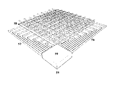
Figure 9, as mentioned displays the superposition of one network (56) of
latitudinal directed elements over another network (57) of longitudinally
directed
elements with a mosaic interlayer supported by a grid substructure (59)
separating the two networks and is the preferred embodiment of the invention.
In
this figure, the signal-processing device (59) may be one device, contrary to
the
depiction in Figure 8. Such device (59) or devices (48, 50) could be a
microcontroller that may be associated with numerous auxiliary devices (not
shown) to allow additional functions. These functions include and are not
limited
to, alarming and wireless communications to other devices.
Figure 10 shows a schematic diagram of the grid of elements formed by
superposition of networks in the preferred embodiment of the invention (55). A
11
CA 02801809 2013-01-14
node (60) represents a terminal at the pulse-generating device of the first
element (61) in the first network travelling along the ordinate and another
node
(62) represents a terminal of the first element (63) in the second network
below
travelling along the abscissa at the pulse-receiving device. Solid lines of
elements represent elements on the plane of the paper, whereas dashed lines of
elements represent elements some distance into the plane of the paper to
signify
the two networks' superposition and their physical separation by the
interlayer
(10). The space between each element will define the resolution of detection,
whereby larger lengths will generate lower resolution. The length of each
element
travelling along the ordinate (62) will define size of area of detection,
where
larger lengths will allow a larger area of detection. The same can be said
with
elements travelling along the abscissa (63).
As discussed previously, the sensor array (55) can be arranged as an
organization of repeated modules (64) where each module (64) comprises of
multiple but possibly different constituents and their associated intersection
of
elements (64a, 64b, 64c, 64d) allow for detection of multiple predetermined
effects across the area of detection. For the sake of clarifying the concept
of a
module (64), the sensor array could be used to detect four predetermined
physical or chemical conditions discussed previously. One module will require
at
least four constituents and thus four intersections (64a, 64h, 64c, 64d),
preferably
in a 2x2 grid. This module (64) or 2x2 grid is repeated over the entirety of
the
sensor array (55). For instance, the constituent corresponding to the
intersection
(64a) at the upper right corner of the module (64) is temperature sensing, and
that of the intersection (64b) at the upper left corner is methane gas sensing
and
that of the intersection (64c) at the bottom left corner is pressure sensing
and
that of the intersection (64d) at the bottom right corner is water sensing. In
the
case where a water leak is to be probed, a systematic check is performed of
all
elements that intersect at the constituent located at the bottom right corner
of
every module (64). This includes every other element beginning from the second
element (65) that travels along the ordinate and every other element beginning
12
CA 02801809 2013-01-14
from the first element (63) that travels along the abscissa. Other
configurations
for a module (64) are possible and are not limited to intersections forming a
square grid, as in the aforementioned case.
In the event of a leak (68) occurring at intersection between elements (66,
67),
detection is possible because the intersection corresponds to the lower left
corner (69d) of a module (69), which is able to detect water. Said detection
is
mediated through signal transmission in the form of a pulse from the pulse-
generating device across the two elements and analyzing changes thereof.
Probing of elements, where one element that travels along the abscissa and one
element along the ordinate, is done in a systematic manner at predetermined
times so as to monitor the entire array for all predetermined effects. Changes
that
occur with transmission of a signal associated with two elements, each
associated with a position along the abscissa and the ordinate allow for
localization of the affected area.
A simplified schematic representation of the means by which selective probing
of
one element from one network and another element through pulse signaling and
TDM is illustrated in Figure 11. The sensor array is represented by a network
of
two elements (75, 76) associated with the pulse generating device (77)
corresponding to different nodes (78, 79) of a circuit switch apparatus (80)
and a
second network of two elements (81, 82) associated with a pulse-receiving-
device (83) corresponding to nodes (84, 85) of a second circuit switch
apparatus
(86). Each circuit switch apparatus (80, 86) can be represented as containing
a
switch (87, 88) that revolves around at different frequencies so as to allow
all
combinations of two different elements (75, 76, 81, 82), where a connection
with
an element (75, 76, 81, 82) is made when the switches (87, 88) come into
contact with corresponding element nodes (84, 85, 78, 79). When contact is
made by the two switches (87, 88) the elements (76, 81) are connected. The
pulse-generating device (77) creates an electrical pulse (89), in this case a
square pulse. In the event that the constituent at the intersection (91) of
the two
13
CA 02801809 2013-01-14
elements (76, 81) is not subject to its corresponding physical or chemical
effect,
a normal pulse (90) is received at the pulse-receiving device. In the event
that
the constituent at the intersection (91) is subject to its corresponding
physical or
chemical effect an altered pulse (92) is transmitted as a result of change in
its
electrical properties. Pulse signaling provides a robust and quick way to
observe
changes within the sensor array. Furthermore the use of TDM and multiple
configurations thereof minimizes requirements for gratuitous amounts of wires
and periphery devices that would otherwise increase the number of failure
points
and malfunctions that could occur, as well as reducing difficulty of
installation. In
addition once installed, other networks of conductors could easily be
installed to
the same signal-processing and multiplexing device in case multiple networks
are required for geometries or several areas at of detection are needed, for
example in artificial environments or structures resident in geographical
sites with
seismic activity and faults. This pulse signaling and multiplexing could be
facilitated by a microcontroller to which other devices may be connected to
allowing some form of output to a user in the event of detection.
14