Note : Les descriptions sont présentées dans la langue officielle dans laquelle elles ont été soumises.
CA 02802453 2013-01-17
42936-CA-PAT
MOBILE WIRELESS COMMUNICATIONS DEVICE WITH IMPEDANCE MATCHING
AND RELATED METHODS
Technical Field
[0001] This application relates to the field of
communications, and more particularly, to wireless
communications systems and related methods.
Background
[0002] Mobile communication systems continue to grow in
popularity and have become an integral part of both personal and
business communications. Various mobile devices now incorporate
Personal Digital Assistant (PDA) features such as calendars,
address books, task lists, calculators, memo and writing
programs, media players, games, etc. These multi-function
devices usually allow electronic mail (email) messages to be
sent and received wirelessly, as well as access the Internet via
a cellular network and/or a wireless local area network (WLAN),
for example.
[0003] Cellular devices have radio frequency (RF) processing
circuits and receive or transmit radio communications signals
typically using modulation schemes. In the typical device, the
RF processing circuits may include a modulator, a power
amplifier coupled downstream from the modulator, and an antenna
coupled downstream from the power amplifier. Depending on the
immediate surroundings of the cellular device, the impedance
load of the antenna may vary, which can impact antenna
performance.
[0004] Some cellular devices include an impedance matching
device between the antenna and the power amplifier to compensate
for the impedance mismatches. One drawback to this approach is
1
CA 02802453 2013-01-17
42936-CA-PAT
= that a phase change is imparted onto the transmitted signal.
Depending on the wireless protocol being used, this may cause
issues with the receiver device.
Brief Description of the Drawings
[0005] FIG. 1 is a schematic block diagram of an example
embodiment of a mobile wireless communications device.
[0006] FIG. 2 is a more detailed schematic block diagram of
the mobile wireless communications device of FIG. 1.
[0007] FIG. 3 is a flowchart illustrating operation of the
mobile wireless communications device of FIG. 1.
[0008] FIG. 4 is a schematic block diagram illustrating
example components for the mobile wireless communications device
of FIG. 1.
Detailed Description of the Preferred Embodiments
[0009] The present description is made with reference to the
accompanying drawings, in which embodiments are shown. However,
many different embodiments may be used, and thus the description
should not be construed as limited to the embodiments set forth
herein. Rather, these embodiments are provided so that this
disclosure will be thorough and complete. Like numbers refer to
like elements throughout.
[0010] Generally speaking, a mobile wireless communications
device may include a processor configured to generate a baseband
signal, a modulator coupled downstream from the processor, and a
power amplifier coupled downstream from the modulator. The
mobile wireless communications device may also include an
antenna, and a tunable antenna matching network coupled between
the power amplifier and the antenna and configured to match an
impedance of the antenna and thereby causing a phase change in
2
CA 02802453 2013-01-17
42936-CA-PAT
an output from the antenna. The processor may be configured to
provide upstream phase change compensation in the baseband
signal for the phase change in the output from the antenna.
[0011] More specifically, the mobile wireless communications
device may further comprise a feedback path between the tunable
antenna matching network and the processor. The tunable antenna
matching network may be configured to dynamically match the
impedance of the antenna. The processor may be configured to
provide the upstream phase change compensation based upon an
inverse of the phase change in the output from the antenna.
[0012] The processor may be configured to provide the
upstream phase change compensation substantially simultaneously
with the phase change in the output from the antenna.
Furthermore, the tunable antenna matching network may be
configured to match the impedance of the antenna substantially
instantaneously.
[0013] In some embodiments, the processor may be configured
to generate digital baseband In-phase (I) and Quadrature (Q)
signals. The modulator may comprise I and Q circuits coupled
between the processor and the power amplifier. Also, each of
the I and Q circuits may comprise a digital-to-analog converter
(DAC), a low pass filter coupled to an output of the DAC, and a
mixer coupled to an output of the low pass filter.
Additionally, the mobile wireless communications device may
further comprise an antenna switch coupled between the power
amplifier and the antenna.
[0014] Another aspect is directed to a method of providing
impedance matching in a mobile wireless communications device.
The mobile wireless communications device may comprise a
processor generating a baseband signal, a modulator coupled
downstream from the processor, a power amplifier coupled
3
CA 02802453 2013-01-17
42936-CA-PAT
downstream from the modulator, an antenna, and a tunable antenna
matching network coupled between the power amplifier and the
antenna. The method may include matching an impedance of the
antenna and thereby causing a phase change in an output from the
antenna using the tunable antenna matching network, and
providing upstream phase change compensation in the baseband
signal for the phase change in the output from the antenna.
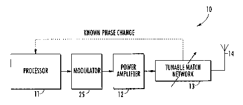
[0015] Referring now to FIG. 1, a mobile wireless
communications device 10 according to the present disclosure is
now described. Moreover, with reference additionally to FIG. 3,
a flowchart 30 illustrates a method of operating the mobile
wireless communications device 10 (Block 31). Example mobile
wireless communications devices may include portable or personal
media players (e.g., music or MP3 players, video players, etc.),
remote controls (e.g., television or stereo remotes, etc.),
portable gaming devices, portable or mobile telephones,
smartphones, tablet computers, etc.
[0016] The mobile wireless communications device 10
illustratively includes a processor 11 configured to generate a
baseband signal, a modulator 25 coupled downstream from the
processor, and a power amplifier 12 coupled downstream from the
modulator. The mobile wireless communications device 10
illustratively includes an antenna 14, and a tunable antenna
matching network 13 coupled between the power amplifier 12 and
the antenna.
[0017] During use, the immediate environment of the mobile
wireless communications device 10 may cause changes in the load
impedance of the antenna 14. For example, the position of the
user's hand may unintentionally change the impedance of the
antenna 14 and cause degraded performance, or the user may place
the mobile wireless communications device 10 on a flat metallic
4
CA 02802453 2013-01-17
42936-CA-PAT
surface, such as a desk. To compensate for this occurrence, the
tunable antenna matching network 13 is configured to match an
impedance of the antenna 14, which causes a phase change in an
output from the antenna 14 (Blocks 33 & 35). In some
communication protocols, such as 3GPP Long Term Evolution (LTE),
there is a threshold/limit to the amount of phase change in a
transmitted signal from a device. Accordingly, in typical
devices, due to phase change resulting from the typical
impedance matching operations, the typical device limits the
speed of impedance matching so as not to violate the
communication protocol phase change threshold. Of course, this
may result in poor performance while the device moves to match
antenna impedance.
[0018] In the illustrated embodiment, the mobile wireless
communications device 10 includes a feedback path between the
tunable antenna matching network 13 and the processor 11. Using
this feedback path, the tunable antenna matching network 13
communicates the phase change in the transmitted signal. The
processor 11 is configured to provide upstream phase change
compensation in the baseband signal for the phase change in the
output from the antenna 14 based upon the data from the feedback
path (Block 37). More specifically, the tunable antenna
matching network 13 is configured to dynamically match the
impedance of the antenna 14, i.e. matching the impedance in real
time and as fast as possible. Advantageously, the processor 11
is configured to provide the upstream phase change compensation
substantially simultaneously with the phase change in the output
from the antenna 14. Furthermore, the tunable antenna matching
network 13 is configured to match the impedance of the antenna
14 substantially instantaneously.
[0019] More specifically, the speed of phase change within
CA 02802453 2013-01-17
42936-CA-PAT
the tunable antenna matching network 13 can be very fast. This
is the reason why the typical device slows down the matching
process. For example, 3GPP wideband code division multiple
access (WCDMA) allows no more than 30 degrees of phase change
within any 666.66 micro-second period. Furthermore, phase
changes larger than 30 degrees can only happen once in any 3
milli-second period, and phase changes larger than 60 degrees
are never allowed. In the mobile wireless communications device
10, the processor 11 would be configured to simultaneously
change the match and correct the phase on the order of 1 micro-
second. This allows the matching to be applied substantially
faster than otherwise possible.
[0020] For example, the processor 11 may be configured to
provide the upstream phase change compensation based upon an
inverse of the phase change in the output from the antenna 14.
In some embodiments, since both magnitude and phase of the
antenna impedance match are unknown, these two pieces of
information are needed to calculate the required impedance
match. The required phase and magnitude change can be
calculated using the forward and reverse voltage waveforms from
a directional coupler (not shown), which is placed before the
antenna 14. The antenna reflection coefficient is a function of
the complex load impedance and the complex source impedance, and
can be shown as: r= (4¨zo) / (zL+zo) = Er/Ei.
[0021] Er and Ei are the reflected and incident voltages
captured from the directional coupler. With Zo, Er, and Ei
known, the load is calculated as: ZL = -Zo * (r+1)/(r-1). Due to
the slowly varying nature of the antenna match, these values can
be monitored at separate times, requiring only one transducer to
digitize the values for calculation. The coupled RF can be
downconverted via an auxiliary receiver and analog-to-digital
6
CA 02802453 2013-01-17
42936-CA-PAT
= converter. With ZL known, the difference in phase from the
previous ZL (ZL') can be calculated. If the new antenna match is
updated instantaneously, the RF phase will also change by the
difference between ZL and ZL,, but if the opposite phase
correction is applied upstream in the digital chain (e.g. at the
processor 11), the RF will not contain any phase change.
Accordingly, the antenna impedance match can be immediately
applied to the antenna 14 without violating the need for small
instantaneous phase changes in the RF (Block 39).
[0022] Referring additionally to FIG. 2, the processor 11 is
configured to generate digital baseband I and Q signals. The
modulator 25 illustratively includes I and Q circuits coupled
between the processor 11 and the power amplifier 12. Also, each
of the I and Q circuits illustratively includes a DAC 15a-15b, a
low pass filter 16a-16b coupled to an output of the DAC, and a
mixer 17a-17b coupled to an output of the low pass filter. The
I circuit includes a local oscillator 18a coupled to the mixer
17a, and the Q circuit includes a local oscillator 18b, and a 90
degrees phase chance block 20 coupled downstream therefrom and
to the mixer 17b. The mobile wireless communications device 10
illustratively includes an adder 19 configured to combine the
modulated I and Q signals, an antenna switch 21 coupled between
the power amplifier 12 and the antenna, and a receiver block 22
coupled between the antenna switch 21 and the processor 11.
[0023] Another aspect is directed to a method of providing
impedance matching in a mobile wireless communications device
10. The mobile wireless communications device 10 may comprise a
processor 11 generating a baseband signal, a modulator 25
coupled downstream from the processor, a power amplifier 12
coupled downstream from the modulator, an antenna 14, and a
tunable antenna matching network 13 coupled between the power
7
CA 02802453 2013-01-17
42936-CA-PAT
amplifier and the antenna. The method may include matching an
impedance of the antenna 14 and thereby causing a phase change
in an output from the antenna using the tunable antenna matching
network 13, and providing upstream phase change compensation for
the phase change in the output from the antenna.
[0024] Example components of a mobile wireless communications
device 1000 that may be used in accordance with the above-
described embodiments are further described below with reference
to FIG. 4. The device 1000 illustratively includes a housing
1200, a keyboard or keypad 1400 and an output device 1600. The
output device shown is a display 1600, which may comprise a full
graphic liquid crystal display (LCD). Other types of output
devices may alternatively be utilized. A processing device 1800
is contained within the housing 1200 and is coupled between the
keypad 1400 and the display 1600. The processing device 1800
controls the operation of the display 1600, as well as the
overall operation of the mobile device 1000, in response to
actuation of keys on the keypad 1400.
[0025] The housing 1200 may be elongated vertically, or may
take on other sizes and shapes (including clamshell housing
structures). The keypad may include a mode selection key, or
other hardware or software for switching between text entry and
telephony entry.
[0026] In addition to the processing device 1800, other parts
of the mobile device 1000 are shown schematically in FIG. 4.
These include a communications subsystem 1001; a short-range
communications subsystem 1020; the keypad 1400 and the display
1600, along with other input/output devices 1060, 1080, 1100 and
1120; as well as memory devices 1160, 1180 and various other
device subsystems 1201. The mobile device 1000 may comprise a
two-way RF communications device having data and, optionally,
8
CA 02802453 2013-01-17
42936-CA-PAT
voice communications capabilities. In addition, the mobile
=
device 1000 may have the capability to communicate with other
computer systems via the Internet.
[0027] Operating system software executed by the processing
device 1800 is stored in a persistent store, such as the flash
memory 1160, but may be stored in other types of memory devices,
such as a read only memory (ROM) or similar storage element. In
addition, system software, specific device applications, or
parts thereof, may be temporarily loaded into a volatile store,
such as the random access memory (RAM) 1180. Communications
signals received by the mobile device may also be stored in the
RAM 1180.
[0028] The processing device 1800, in addition to its
operating system functions, enables execution of software
applications 1300A-1300N on the device 1000. A predetermined
set of applications that control basic device operations, such
as data and voice communications 1300A and 13003, may be
installed on the device 1000 during manufacture. In addition, a
personal information manager (PIN) application may be installed
during manufacture. The PIN may be capable of organizing and
managing data items, such as e-mail, calendar events, voice
mails, appointments, and task items. The PIN application may
also be capable of sending and receiving data items via a
wireless network 1401. The PIN data items may be seamlessly
integrated, synchronized and updated via the wireless network
1401 with corresponding data items stored or associated with a
host computer system.
[0029] Communication functions, including data and voice
communications, are performed through the communications
subsystem 1001, and possibly through the short-range
communications subsystem 1020. The communications subsystem
9
CA 02802453 2013-01-17
42936-CA-PAT
1001 includes a receiver 1500, a transmitter 1520, and one or
more antennas 1540 and 1560. In addition, the communications
subsystem 1001 also includes a processing module, such as a
digital signal processor (DSP) 1580, and local oscillators (L0s)
1601. The specific design and implementation of the
communications subsystem 1001 is dependent upon the
communications network in which the mobile device 1000 is
intended to operate. For example, a mobile device 1000 may
include a communications subsystem 1001 designed to operate with
the MobitexTM, Data TACm or General Packet Radio Service (GPRS)
mobile data communications networks, and also designed to
operate with any of a variety of voice communications networks,
such as Advanced Mobile Phone System (AMPS), time division
multiple access (TDMA), code division multiple access (CDMA),
Wideband code division multiple access (W-CDMA), personal
communications service (PCS), GSM (Global System for Mobile
Communications), enhanced data rates for GSM evolution (EDGE),
etc. Other types of data and voice networks, both separate and
integrated, may also be utilized with the mobile device 1000.
The mobile device 1000 may also be compliant with other
communications standards such as 3GSM, 3rd Generation
Partnership Project (3GPP), Universal Mobile Telecommunications
System (UMTS), 4G, etc.
[0030] Network access requirements vary depending upon the
type of communication system. For example, in the Mobitex and
DataTAC networks, mobile devices are registered on the network
using a unique personal identification number or PIN associated
with each device. In GPRS networks, however, network access is
associated with a subscriber or user of a device. A GPRS device
therefore typically involves use of a subscriber identity
module, commonly referred to as a SIN card, in order to operate
CA 02802453 2013-01-17
42936-CA-PAT
on a GPRS network.
[0031] When required network registration or activation
procedures have been completed, the mobile device 1000 may send
and receive communications signals over the communication
network 1401. Signals received from the communications network
1401 by the antenna 1540 are routed to the receiver 1500, which
provides for signal amplification, frequency down conversion,
filtering, channel selection, etc., and may also provide analog
to digital conversion. Analog-to-digital conversion of the
received signal allows the DSP 1580 to perform more complex
communications functions, such as demodulation and decoding. In
a similar manner, signals to be transmitted to the network 1401
are processed (e.g. modulated and encoded) by the DSP 1580 and
are then provided to the transmitter 1520 for digital to analog
conversion, frequency up conversion, filtering, amplification
and transmission to the communication network 1401 (or networks)
via the antenna 1560.
[0032] In addition to processing communications signals, the
DSP 1580 provides for control of the receiver 1500 and the
transmitter 1520. For example, gains applied to communications
signals in the receiver 1500 and transmitter 1520 may be
adaptively controlled through automatic gain control algorithms
implemented in the DSP 1580.
[0033] In a data communications mode, a received signal, such
as a text message or web page download, is processed by the
communications subsystem 1001 and is input to the processing
device 1800. The received signal is then further processed by
the processing device 1800 for an output to the display 1600, or
alternatively to some other auxiliary I/O device 1060. A device
may also be used to compose data items, such as e-mail messages,
using the keypad 1400 and/or some other auxiliary I/O device
11
CA 02802453 2013-01-17
42936-CA-PAT
1060, such as a touchpad, a rocker switch, a thumb-wheel, or
=
some other type of input device. The composed data items may
then be transmitted over the communications network 1401 via the
communications subsystem 1001.
[0034] In a voice communications mode, overall operation of
the device is substantially similar to the data communications
mode, except that received signals are output to a speaker 1100,
and signals for transmission are generated by a microphone 1120.
Alternative voice or audio I/O subsystems, such as a voice
message recording subsystem, may also be implemented on the
device 1000. In addition, the display 1600 may also be utilized
in voice communications mode, for example to display the
identity of a calling party, the duration of a voice call, or
other voice call related information.
[0035] The short-range communications subsystem enables
communication between the mobile device 1000 and other proximate
systems or devices, which need not necessarily be similar
devices. For example, the short-range communications subsystem
may include an infrared device and associated circuits and
components, a Bluetoothlm communications module to provide for
communication with similarly-enabled systems and devices, or a
NFC sensor for communicating with a NFC device or NFC tag via
NFC communications.
[0036] Many modifications and other embodiments will come to
the mind of one skilled in the art having the benefit of the
teachings presented in the foregoing descriptions and the
associated drawings. Therefore, it is understood that various
modifications and embodiments are intended to be included within
the scope of the appended claims.
12