Sélection de la langue

Search

Sommaire du brevet 2807122 

Énoncé de désistement de responsabilité concernant l'information provenant de tiers

Une partie des informations de ce site Web a été fournie par des sources externes. Le gouvernement du Canada n'assume aucune responsabilité concernant la précision, l'actualité ou la fiabilité des informations fournies par les sources externes. Les utilisateurs qui désirent employer cette information devraient consulter directement la source des informations. Le contenu fourni par les sources externes n'est pas assujetti aux exigences sur les langues officielles, la protection des renseignements personnels et l'accessibilité.

Disponibilité de l'Abrégé et des Revendications

L'apparition de différences dans le texte et l'image des Revendications et de l'Abrégé dépend du moment auquel le document est publié. Les textes des Revendications et de l'Abrégé sont affichés :

  • lorsque la demande peut être examinée par le public;
  • lorsque le brevet est émis (délivrance).
(12) Brevet: (11) CA 2807122
(54) Titre français: COMPOSANT OPTIQUE
(54) Titre anglais: OPTICAL COMPONENT
Statut: Accordé et délivré
Données bibliographiques
(51) Classification internationale des brevets (CIB):
  • G02B 06/30 (2006.01)
  • G02B 06/122 (2006.01)
(72) Inventeurs :
  • ISHII, MOTOHAYA (Japon)
  • YAMADA, TAKASHI (Japon)
  • DOI, YOSHIYUKI (Japon)
  • SAIDA, TAKASHI (Japon)
  • TSUZUKI, KEN (Japon)
  • GOH, TAKASHI (Japon)
  • YAMAZAKI, HIROSHI (Japon)
  • MINO, SHINJI (Japon)
  • FUKUMITSU, TAKAO (Japon)
  • MURASAWA, ATSUSHI (Japon)
  • EBISAWA, FUMIHIRO (Japon)
  • TERUI, HIROSHI (Japon)
  • SHIBAZAKI, TOMOYO (Japon)
  • KIKUCHI, YUICHI (Japon)
(73) Titulaires :
  • NTT ELECTRONICS CORPORATION
  • NIPPON TELEGRAPH AND TELEPHONE CORPORATION
(71) Demandeurs :
  • NTT ELECTRONICS CORPORATION (Japon)
  • NIPPON TELEGRAPH AND TELEPHONE CORPORATION (Japon)
(74) Agent: SMART & BIGGAR LP
(74) Co-agent:
(45) Délivré: 2015-06-09
(86) Date de dépôt PCT: 2011-08-02
(87) Mise à la disponibilité du public: 2012-02-09
Requête d'examen: 2013-01-30
Licence disponible: S.O.
Cédé au domaine public: S.O.
(25) Langue des documents déposés: Anglais

Traité de coopération en matière de brevets (PCT): Oui
(86) Numéro de la demande PCT: PCT/JP2011/004375
(87) Numéro de publication internationale PCT: JP2011004375
(85) Entrée nationale: 2013-01-30

(30) Données de priorité de la demande:
Numéro de la demande Pays / territoire Date
2010-177979 (Japon) 2010-08-06

Abrégés

Abrégé français

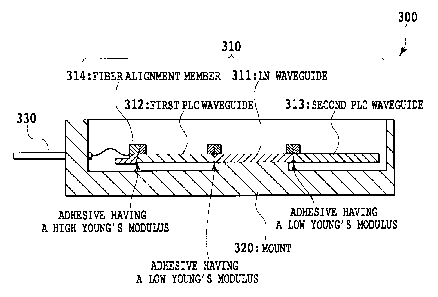
L'invention vise à supprimer la détérioration de fiabilité due à une contrainte thermique dans un composant optique, dans lequel une puce d'élément optique est fixée sur une monture, ladite puce d'élément optique ayant une pluralité d'éléments optiques du type guide d'ondes ayant des coefficients de dilatation thermique différents se faisant mutuellement face et connectés à l'intérieur de celle-ci. Un composant optique (300) comporte : une puce d'élément optique (310), qui comporte un guide d'ondes à faible bruit (311), un premier guide d'ondes PLC (312) relié à une extrémité du guide d'ondes à faible bruit (311), un second guide d'ondes PLC (313) relié à l'autre extrémité du guide d'ondes à faible bruit (311), et un élément d'alignement de fibre (314) relié au premier guide d'ondes PLC (312) ; une monture (320) ayant la puce d'élément optique (310) fixée à celle-ci ; et une fibre optique (330) alignée à l'aide de l'élément d'alignement de fibre (314). La surface de liaison entre le premier guide d'ondes PLC (312) et l'élément d'alignement de fibre (314) a une structure inclinée, et les surfaces de liaison entre le guide d'ondes à faible bruit (311) et les premier et second guides d'ondes PLC (312, 313) ont des structures à angle droit. Dans la structure à angle droit, les guides d'ondes sont reliés avec un adhésif ayant un module d'Young inférieur à celui d'un adhésif sur la surface de liaison dans la structure inclinée.


Abrégé anglais


In an optical component configured to fix to a mount an
optical device chip in which waveguide type optical devices
having different thermal expansion coefficients are
butt-jointed, deterioration in reliability due to thermal
stress is suppressed. The optical component comprises an
optical device chip including an LN waveguide, a first PLC
waveguide, a second PLC waveguide, and a fiber alignment member,
a mount, and optical fibers. Each of connection faces between
the first PLC waveguide and the fiber alignment member is
configured as a tilted structure, and each of connection faces
between the LN waveguide, and the first and second PLC waveguides
is configured as a right-angled structure. In the right-angled
structure, the connection faces are connected by an adhesive
having a lower Young's modulus than that of an adhesive used
on the connection faces of the tilted structure.

Revendications

Note : Les revendications sont présentées dans la langue officielle dans laquelle elles ont été soumises.


CLAIMS
1. An optical component comprising:
an optical device chip including a first waveguide type optical
device, a second waveguide type optical device which is
butt-jointed to an end of the first waveguide type optical device
to be optically coupled therewith and has a thermal expansion
coefficient different from that of the first waveguide type
optical device, and a fiber alignment member butt-jointed to
the second waveguide type optical device to be optically coupled
therewith;
a mount on which the optical device chip is mounted; and
one or more optical fibers aligned to the fiber alignment member
and fixed in a buckled state, wherein
each of connection faces between the second waveguide type
optical device and the fiber alignment member is configured as
a tilted structure,
each of connection faces between the first waveguide type optical
device and the second waveguide type optical device is configured
as a right-angled structure,
the adhesive used on the connection face of the tilted structure
suppresses an optical axis shift on the connection face of the
tilted structure due to buckling stress of the optical fiber,
the adhesive used on the connection face of the right-angled
structure suppresses separation of adhesive faces between the
first waveguide type optical device and the second waveguide
type optical device due to thermal strain, and
-13-

a Young's modulus of an adhesive used on the connection face
of the tilted structure is higher than that of an adhesive used
on the connection face of the right-angled structure.
2. An optical component according to claim 1, wherein
the Young's modulus of the adhesive used on the connection face
of the tilted structure is equal to or more than 1 x 10 7 Pa, and
the Young's modulus of the adhesive used on the connection face
of the right-angled structure is less than 1 x 10 7 Pa.
3. An optical component according to claim 2, wherein
a difference in thermal expansion coefficient between the
second waveguide type optical device and the fiber alignment
member is smaller than a difference in thermal expansion
coefficient between the first waveguide type optical device and
the second waveguide type optical device.
4. An optical component according to claim 2, wherein
a substrate of the first waveguide type optical device is
made of lithium niobate, indium phosphorus or KTN, and
a substrate of the second waveguide type optical device is made
of quartz or silicon.
5. An optical component according to claim 3, wherein
a substrate of the first waveguide type optical device is
made of lithium niobate, indium phosphorus or KTN, and
a substrate of the second waveguide type optical device is made
of quartz or silicon.
-14-

Description

Note : Les descriptions sont présentées dans la langue officielle dans laquelle elles ont été soumises.


CA 02807122 2013-01-30
DESCRIPTION
OPTICAL COMPONENT
Technical Field
[0001]
The present invention relates to an optical component,
and in more detail, to an optical component provided with a
waveguide type optical device.
Background Art
[0002]
With the development of optical communication systems,
the demand for highly-functional optical modules (optical
components) increases. A waveguide type optical device can
realize various kinds of lightwave circuits by forming
waveguides on a substrate, which is used as an element of the
optical module. For higher functionality of the optical module,
a hybrid optical module, in which waveguide type optical devices
having different functions are integrated, is realized. An
example of a specific optical module includes an RZ-DQPSK
(Return to Zero Differential Quadrature Phase Shift Keying)
module and the like.
[0003]
The RZ-DQPSK module has the structure, for example, that
PLC (Planar Lightwave Circuit) waveguides each forming an
optical waveguide on an Si substrate or a quarts substrate by
silica-based glass and an LN waveguide forming optical
- 1 -

CA 02807122 2013-01-30
waveguides on an LN (lithium niobate) substrate by using
titanium diffusion are butt-jointed so as to be optically
coupled, and the LN waveguide is fixed to a mount (refer to Fig.
lA and Fig. 13) . In Fig. lA and Fig. 1B (corresponding to Fig.
6 in Non-Patent Literature 1) , the mount achieves a function
of a package accommodating the PLC waveguides, the LN waveguide,
and a fiber alignment member. Optical fibers are aligned to
the fiber alignment member and are butt-jointed thereto to be
optically coupled with the PLC waveguide. Connection
interfaces between the fiber alignment member and the PLC
waveguide and between the PLC waveguide and the LN waveguide
are respectively fixed by an adhesive. In addition, the optical
fibers are fixed to the mount in a position of penetrating
through the mount by soldering or the like. In such a structure,
as a temperature in the periphery of the optical module changes,
a thermal strain is generated due to a difference in thermal
expansion between the respective materials in each of the
connection interfaces between the fiber alignment member and
the PLC waveguide and between the PLC waveguide and the LN
waveguide, which therefore causes the adhesive to be easily
separated. Further, a difference in thermal expansion between
each of the PLC waveguide and the LN waveguide, and the mount
is generated, thus applying tension stress on the optical fiber.
An increase in the tensile stress causes breakdown of the
optical fiber. Even if a material of the mount (package) is
made of stainless, for example, SUS303 to make a difference in
thermal expansion coefficient from the LN smaller, a large
- 2 -

CA 02807122 2013-01-30
difference in the thermal expansion coefficient exists between
the PLC, the optical fiber or the like, and the package material.
Table 1 shows values of the thermal expansion coefficient. For
overcoming this problem, a soft adhesive for relaxation of the
thermal stress is used in each of the connection interfaces
between the fiber alignment member and the PLC waveguide and
between the PLC waveguide and the LN waveguide to prevent the
separation therein. In addition, as shown in Fig. 1B, there
is adopted a method where the optical fiber is buckled to release
the thermal stress to be applied on the optical fiber.
[0004]
[Table 1]
Name of Component Thermal expansion coefficient
(x10-6/K)
SUS303 17.3
LN 15.4
PLC 2.5
Optical fiber 0.75
Citation List
Non-Patent Literature
[0005]NPL 1: Technical report by Institute of Electronics,
Information and Communication Engineers of 2005/May20, Vol . 105 ,
No.71, pp. 1 to 6, 0PE2005-8: Highly functional and high-speed
modulatows with PLC-LiNb03 direct attachment, by Takashi Yamada
and Motohaya Ishii
- 3 -

CA 02807122 2013-01-30
Summary of Invention
[0006]
The aforementioned structure has, however, still the
problem. Each of the connection portions between the PLC
waveguide and the fiber alignment member generally adopts the
structure of preventing reflection by tilting an end face
thereof. Therefore the buckling stress of the fiber is
generated to cause a component in parallel to each of the
connection faces between the PLC waveguide and the fiber
alignment member where a soft adhesive is used, and the parallel
component is the cause of an optical axis shift (refer to Fig.
2). Particularly in Fig. 2, Pb is the buckling stress applied
from the fiber to the fiber alignment member, and is expressed
according to Formula (1).
[0007]
[Formula 1]
4g2EI 1r (1)
L2 64
[0008]
where L is the fiber length, E is the Young's modulus, I is second
moment of area (quantity expressing a degree in difficulty of
deformation of an object to bending moment), and d is the
diameter.
[0009]
In the above description, the explanation is made of an
example of the RZ-DQPSK module in which the PLC-LN chip
configured by the PLC waveguides and the LN waveguide is fixed
- 4 -

=
CA 02807122 2013-01-30
to the mount, but the similar problem takes place with
respect to an optical device chip in which a plurality of
waveguide type optical devices having different thermal
expansion coefficients are butt-jointed.
[0010]
The present invention is made in view of the foregoing
problem, it may therefore be desirable to suppress
deterioration in reliability due to thermal stress in an
optical component fixed to a mount, and the optical
component comprises an optical device chip, in which a
plurality of waveguide type optical devices having different
thermal expansion coefficients are butt-jointed, and one or
more optical fibers.
[0011]
An optical component according to a first aspect in the
present invention, comprises an optical device chip
including a first waveguide type optical device, a second
waveguide type optical device which is butt-jointed to an
end of the first waveguide type optical device to be
optically coupled therewith and has a thermal expansion
coefficient different from that of the first waveguide type
optical device, and a fiber alignment member butt-jointed to
the second waveguide type optical device to be optically
coupled therewith, a mount on which the optical device chip
is mounted, and one or more optical fibers aligned to the
fiber alignment member and fixed in a buckled state, wherein
each of connection faces between the second waveguide type
optical device and the fiber alignment member is configured
as a tilted
-5-

CA 02807122 2013-01-30
structure, each of connection faces between the first waveguide
type optical device and the second waveguide type optical device
is configured as a right-angled structure, the adhesive used
on the connection face of the tilted structure suppresses an
optical axis shift on the connection face of the tilted
structure due to buckling stress of the optical fiber, and the
adhesive used on the connection face of the right-angled
structure suppresses separation of adhesive faces between the
first waveguide type optical device and the second waveguide
type optical device due to thermal strain, a Young's modulus
of an adhesive used on the connection face of the tilted
structure is higher than that of an adhesive used on the
connection face of the right-angled structure.
[0012]
In addition, a second aspect of the present invention
according to the first aspect is characterized in that the
Young's modulus of the adhesive used on the connection face of
the tilted structure is equal to or more than 1 x 10⁷Pa, and
the Young's modulus of the adhesive used on the connection face
of the right-angled structure is less than 1 x 10⁷Pa.
[0013]
In addition, a third aspect of the present invention
according to the second aspect is characterized in that a
difference in thermal expansion coefficient between the second
waveguide type optical device and the fiber alignment member
is smaller than a difference in thermal expansion coefficient
- 6 -

CA 02807122 2013-01-30
between the first waveguide type optical device and the second
waveguide type optical device.
[0014]
In addition, a fourth aspect of the present invention
according to the second or third aspect is characterized in that
a substrate of the first waveguide type optical device is made
of lithium niobate, indium phosphorus or KTN, and a substrate
of the second waveguide type optical device is made of quartz
or silicon.
[0015]
According to the present invention, in the optical
component comprising the plurality of the waveguide type
optical devices, and the optical fibers fixed in a buckled state
using the fiber alignment member, each of the connection faces
between the waveguide type optical device and the fiber
alignment member is configured as the tilted structure, and each
of the connection faces between the waveguide type optical
devices each other is configured as the right-angled structure,
wherein the Young's modulus of the adhesive used on the
connection face of the tilted structure is higher than that of
the adhesive used on the connection face of the right-angled
structure, thereby making it possible to suppress deterioration
in reliability due to thermal stress.
Brief Description of Drawings
[0016]
- 7 -

CA 02807122 2013-01-30
[Fig. 1A] Fig. 1A is a top view of the conventional optical
component;
[Fig. 1B]Fig. 1B is a cross section taken along line TB
- IB of the conventional optical component;
[Fig. 2]Fig. 2 is a diagram explaining a buckling weight
of an optical fiber;
[Fig. 3]Fig. 3 is a diagram showing an optical component
according to an embodiment in the present invention; and
[Fig. 4]Fig. 4 is a diagram explaining an angle of an
optical waveguide on connection faces between an LN waveguide
and a PLC waveguide.
Description of Embodiments
[0017]
Hereinafter, an embodiment in the present invention will
be in detail explained with reference to the drawings.
[0018]
Fig. 3 shows an optical component according to an
embodiment in the present invention. An optical component 300
is mostly similar to the optical component 100 in Fig. lA and
Fig. 1B, but differs in connection faces between PLC waveguides
and an LN waveguide and in connection faces between the PLC
waveguide and a fiber alignment member therefrom. The optical
component 300 comprises an optical device chip 310 including
an LN waveguide 311 (corresponding to a first waveguide type
optical device), a first PLC waveguide 312 (corresponding to
a second waveguide type optical device) butt-jointed to an end
- 8 -

CA 02807122 2013-01-30
of the LN waveguide 311 to be optically-coupled therewith, a
second PLC waveguide 313 butt-jointed to the other end of the
LN waveguide 311 to be optically-coupled therewith, and a fiber
alignment member 314 butt-jointed to the first PLC waveguide
312 to be optically-coupled therewith, amount 320 on which the
optical device chip 310 is mounted, and optical fibers aligned
to the fiber alignment member 314. In Fig. 3, the LN waveguide
311 is fixed to the mount 320, but the first and second waveguides
312 and 313 or the fiber alignment member 314 may be fixed
thereto.
[0019]
As similar to the case in Fig. 1B, a buckling weight Pb
is generated due to buckling of the optical fiber 330, so that
a weighted component exists in a direction in parallel to each
of connection faces between the first PLC waveguide 312 and the
fiber alignment member 314, that is, in a direction of causing
an optical axis shift to the optical component 300. In the
optical component 300 in the present embodiment, the optical
axis shift is suppressed by connecting the connection faces by
an adhesive having a high Young's modulus E (for example, 1 x
107Pa or more). It is preferable that as the fiber alignment
member 314, a material matched to a thermal expansion
coefficient of the first PLC waveguide 312 is selected to
prevent generation of a difference in thermal expansion
coefficient between both sides of connection faces of both. For
example, in a case where a substrate of the first PLC waveguide
- 9 -

, CA 02807122 2013-01-30
312 is formed of Si, Pyrex (registered trademark) glass may be
used in the fiber alignment member 314.
[0020]
In the connection faces between the LN waveguide 311, and
the first and second PLC waveguides 312 and 313, the connection
face is configured as a right-angled structure at a right angle
to the optical axis direction. Since each of the connection
faces between the first PLC waveguide 312 and the fiber
alignment member 314 is configured as the tilted structure, the
force component in parallel to the connection face is generated,
but the force component is eliminated by configuring the
connection face as the right-angled structure. In this case,
it is preferable that they are connected by an adhesive having
a lower Young's modulus than that in the connection interface
between the first PLC waveguide 312 and the fiber alignment
member 314. The reason for it is that, since the LN waveguide
311 differs in thermal expansion coefficient from the first and
second PLC waveguides 312 and 313, as an adhesive having a higher
Young's modulus is used, there is a possibility that the
adhesive faces are separated due to thermal strain. In other
words, when the difference in thermal expansion coefficient
exists between both the sides of the connection faces, it is
preferable to use an adhesive having a lower Young's modulus
as the difference becomes larger.
[0021]
In general, there are some cases where each of the
connection faces between the PLC waveguide and the LN waveguide
- 10 -

CA 02807122 2013-01-30
is tilted for reflection prevention, but configuring the
connection face as the right-angled structure as the present
invention also enables the reflection prevention to be realized.
Optical waveguides between the LN waveguide 311, and the first
and second PLC waveguides 312 and 313 are only required to be
designed to have a predetermined angle at the end face. The
reflection prevention will be explained with reference to Fig.
4 by focusing attention on the boundary face between the first
PLC waveguide 312 and the LN waveguide 311. (1) First, a first
angle 01 is determined in such a manner that Fresnel reflection
R expressed according to Formula (2) is not coupled with the
optical waveguide of the first PLC waveguide 312 as returning
light. The first angle 01 is an angle of the optical waveguide
of the first PLC waveguide 312 to a normal line of the connection
face, generally in a range from four degrees to twelve degrees.
[0022]
[Formula 2]
R= n1-n2 \ 2 (2)
n1 +n2)
[0023]
(2) Next, in a case where a refraction index of the first
PLC waveguide 312 is different from that of the LN waveguide
311, a second angle 02 is determined to meet Snell's law
expressed according to Formula (3), wherein nl and n2
respectively indicate refraction indexes of the first PLC
waveguide 312 and the LN waveguide 311.
- 11 -

CA 02807122 2013-01-30
[0024]
[Formula 3]
sin 01 n2
sin 02 (3)
[0025]
The angles 01 and 02 of the optical waveguide are
determined by the above procedure, and thereby the reflection
can be prevented even if the end face is formed of the right
angle.
[0026]
It should be noted that quartz or silicon may be used as
the substrate of each of the first and second PLC waveguides
312 and 313. In addition, a waveguide type optical device
formed on an indium phosphorus substrate or a KTN substrate may
be used instead of the LN waveguide 311.
- 12 -

Dessin représentatif
Une figure unique qui représente un dessin illustrant l'invention.
États administratifs

2024-08-01 : Dans le cadre de la transition vers les Brevets de nouvelle génération (BNG), la base de données sur les brevets canadiens (BDBC) contient désormais un Historique d'événement plus détaillé, qui reproduit le Journal des événements de notre nouvelle solution interne.

Veuillez noter que les événements débutant par « Inactive : » se réfèrent à des événements qui ne sont plus utilisés dans notre nouvelle solution interne.

Pour une meilleure compréhension de l'état de la demande ou brevet qui figure sur cette page, la rubrique Mise en garde , et les descriptions de Brevet , Historique d'événement , Taxes périodiques et Historique des paiements devraient être consultées.

Historique d'événement

Description Date
Représentant commun nommé 2019-10-30
Requête pour le changement d'adresse ou de mode de correspondance reçue 2018-03-28
Requête visant le maintien en état reçue 2015-06-17
Accordé par délivrance 2015-06-09
Inactive : Page couverture publiée 2015-06-08
Préoctroi 2015-03-19
Inactive : Taxe finale reçue 2015-03-19
Un avis d'acceptation est envoyé 2015-01-19
Lettre envoyée 2015-01-19
Un avis d'acceptation est envoyé 2015-01-19
Inactive : Q2 réussi 2014-12-31
Inactive : Approuvée aux fins d'acceptation (AFA) 2014-12-31
Modification reçue - modification volontaire 2014-10-24
Requête visant le maintien en état reçue 2014-07-08
Modification reçue - modification volontaire 2013-12-02
Requête visant le maintien en état reçue 2013-07-05
Inactive : Page couverture publiée 2013-04-05
Inactive : Acc. récept. de l'entrée phase nat. - RE 2013-03-07
Inactive : CIB attribuée 2013-03-07
Demande reçue - PCT 2013-03-07
Inactive : CIB en 1re position 2013-03-07
Lettre envoyée 2013-03-07
Exigences pour l'entrée dans la phase nationale - jugée conforme 2013-01-30
Exigences pour une requête d'examen - jugée conforme 2013-01-30
Modification reçue - modification volontaire 2013-01-30
Toutes les exigences pour l'examen - jugée conforme 2013-01-30
Demande publiée (accessible au public) 2012-02-09

Historique d'abandonnement

Il n'y a pas d'historique d'abandonnement

Taxes périodiques

Le dernier paiement a été reçu le 2014-07-08

Avis : Si le paiement en totalité n'a pas été reçu au plus tard à la date indiquée, une taxe supplémentaire peut être imposée, soit une des taxes suivantes :

  • taxe de rétablissement ;
  • taxe pour paiement en souffrance ; ou
  • taxe additionnelle pour le renversement d'une péremption réputée.

Les taxes sur les brevets sont ajustées au 1er janvier de chaque année. Les montants ci-dessus sont les montants actuels s'ils sont reçus au plus tard le 31 décembre de l'année en cours.
Veuillez vous référer à la page web des taxes sur les brevets de l'OPIC pour voir tous les montants actuels des taxes.

Titulaires au dossier

Les titulaires actuels et antérieures au dossier sont affichés en ordre alphabétique.

Titulaires actuels au dossier
NTT ELECTRONICS CORPORATION
NIPPON TELEGRAPH AND TELEPHONE CORPORATION
Titulaires antérieures au dossier
ATSUSHI MURASAWA
FUMIHIRO EBISAWA
HIROSHI TERUI
HIROSHI YAMAZAKI
KEN TSUZUKI
MOTOHAYA ISHII
SHINJI MINO
TAKAO FUKUMITSU
TAKASHI GOH
TAKASHI SAIDA
TAKASHI YAMADA
TOMOYO SHIBAZAKI
YOSHIYUKI DOI
YUICHI KIKUCHI
Les propriétaires antérieurs qui ne figurent pas dans la liste des « Propriétaires au dossier » apparaîtront dans d'autres documents au dossier.
Documents

Pour visionner les fichiers sélectionnés, entrer le code reCAPTCHA :


Pour visualiser une image, cliquer sur un lien dans la colonne description du document. Pour télécharger l'image (les images), cliquer l'une ou plusieurs cases à cocher dans la première colonne et ensuite cliquer sur le bouton "Télécharger sélection en format PDF (archive Zip)" ou le bouton "Télécharger sélection (en un fichier PDF fusionné)".

Liste des documents de brevet publiés et non publiés sur la BDBC .

Si vous avez des difficultés à accéder au contenu, veuillez communiquer avec le Centre de services à la clientèle au 1-866-997-1936, ou envoyer un courriel au Centre de service à la clientèle de l'OPIC.


Description du
Document 
Date
(aaaa-mm-jj) 
Nombre de pages   Taille de l'image (Ko) 
Description 2013-01-29 12 369
Revendications 2013-01-29 2 60
Dessins 2013-01-29 3 47
Abrégé 2013-01-29 1 33
Dessin représentatif 2013-01-29 1 14
Revendications 2013-01-30 2 63
Description 2013-01-30 12 369
Abrégé 2013-01-30 1 22
Dessin représentatif 2015-05-18 1 11
Paiement de taxe périodique 2024-07-01 30 1 219
Accusé de réception de la requête d'examen 2013-03-06 1 177
Avis d'entree dans la phase nationale 2013-03-06 1 203
Courtoisie - Certificat d'enregistrement (document(s) connexe(s)) 2013-03-06 1 104
Rappel de taxe de maintien due 2013-04-02 1 114
Avis du commissaire - Demande jugée acceptable 2015-01-18 1 162
PCT 2013-01-29 8 426
Taxes 2013-07-04 2 77
Taxes 2014-07-07 2 79
Correspondance 2015-03-18 2 75
Paiement de taxe périodique 2015-06-16 2 81