Note : Les descriptions sont présentées dans la langue officielle dans laquelle elles ont été soumises.
INTEGRATED CIRCUIT WITH PROGRAMMABLE LOGIC ANALYZER,
ENHANCED ANALYZING AND DEBUGGING CAPABILITIES AND METHOD
CROSS REFERENCE TO RELATED APPLICATION
Pursuant to 37 C.F.R. 1.78, this application is a continuation-in-part
application and claims the benefit of the earlier filing date of Application
Serial No.
12/542.976, filed August 18, 2009, entitled "An Integrated Circuit Including a
Programmable
Logic Analyzer with Enhanced Analyzing and Debugging Capabilities and a Method
Therefor".
BACKGROUND
1. FIELD OF THE INVENTION
[00011 The present invention relates generally to an embedded logic
analyzer, and
particularly to a programmable embedded logic analyzer for analyzing an
electronic circuit.
2. DESCRIPTION OF THE RELATED ART
[0002] A logic analyzer is an electronic instrument that is used to capture
and display
data signals of an electronic circuit. Generally, the logic analyzer captures
the data signals
that are too fast to be observed by a user. The user observes the data signals
captured by the
logic analyzer to effectively analyze the electronic circuit and to take
preemptive actions or to
debug based on the analysis.
[0003] Logic Analyzers may be broadly classified as external logic
analyzers and
embedded logic analyzers. The embedded logic analyzer is generally included
within a
programmable logic device or an integrated circuit (tC), e.g., a complex
programmable logic
device (CPLD), field programmable gate array (FPGA), application specific
integrated circuit
(AS1C), etc. The embedded logic analyzer has the ability to capture large
amounts of high
speed data signals within the IC.
[0004] The embedded logic analyzer may include a memory to store the
captured data
signals. Usually, the embedded logic analyzer is programmable to capture and
store the data
signals specified by the user. The data signals stored by the embedded logic
analyzer may be
transferred to a computer for further analysis. The data signals are generally
transferred to
the computer through an interface provided on the IC.
1
CA 2807323 2017-09-08
CA 02807323 2013-01-31
WO 2012/033876 PCT/US2011/050761
[0005] Fig. 1 is a block diagram of a conventional embedded logic
analyzer (ELA)
100 included within an integrated circuit (not shown). The ELA 100 includes an
interconnect
module 110 to receive a plurality of data signals within the integrated
circuit. The
interconnect module 110 is programmable to select a plurality of signals to be
sampled and at
least one trigger signal to enable sampling from the plurality of received
signals. The at least
one trigger signal is transferred to a trigger module 120. The trigger module
120 is
programmable to set a trigger condition and to detect if the at least one
trigger signal satisfies
the trigger condition. If the trigger condition is satisfied, the trigger
module 120 initiates a
sampling process. Upon the initiation of the sampling process, a memory
controller 130
starts sampling the plurality of signals to be sampled from the interconnect
module 110. The
sampled signals may be stored in a memory 140 for further analysis. Therefore,
the ELA 100
operates to execute a general code given below:
IF (<TRIGGER CONDITION>) THEN (SAMPLE SIGNALS(X)),
wherein the TRIGGER CONDITION is any logical operation or a series of logical
operations
and the SIGNALS (X) are the plurality of signals to be sampled from the
interconnect
module 110. According to the code executed by the ELA 100, when the trigger
condition is
satisfied, the ELA 100 samples at least one sampled signal and stores the
sampled signal in
the memory 140.
[0006] However, the ELA is unable to execute an action other than
sampling when
the trigger condition is satisfied. Further, conventional ELAs do not capture,
analyze, and/or
debug software data or firmware data signals within the IC, and additional
instrument(s) may
be necessary in order to analyze these types of data. Additionally, in order
to program the
ELA or to analyze the data stored within the ELA, the user is required to be
present at a
workstation where the ELA is installed.
[0007] It would be desirable therefore to provide an ELA with enhanced
analyzing
and debugging capabilities to obviate the above-mentioned problems.
SUMMARY
[0008] Exemplary embodiments of the present disclosure overcome the
shortcomings
in known logic analyzers and thereby satisfy a significant need for a
mechanism for
effectively testing and debugging a system. In accordance with an exemplary
embodiment,
there is disclosed an integrated circuit communicatively coupled within a
system, the
integrated circuit including a logic analyzer having an input receiving a
plurality of signals
2
CA 02807323 2013-01-31
WO 2012/033876
PCT/US2011/050761
and an output for providing an indication of the detection, by the logic
analyzer, of at least
one trigger event relative to at least one of the received signals. The
integrated circuit further
includes a built in self test (BIST) block having a first input for receiving
one or more of the
signals appearing at the input of the logic analyzer, and a second input
coupled to the output
of the logic analyzer for selectively enabling the BIST block. The BIST block
generates and
maintains a signature therein based upon the first and second inputs of the
BIST block. By
maintaining a generated signature based upon the one or more signals appearing
at the input
of the logic analyzer and providing the generated signature thereto for event
triggering or
sampling and storage therein, the logic analyzer is able to more effectively
test and debug the
system.
[0009] Additional features and advantages will be set forth in the
detailed description
which follows, and in part will be readily apparent to those skilled in the
art from that
description or recognized by practicing the invention as described herein,
including the
detailed description which follows, the claims, as well as the appended
drawings.
[0010] It is to be understood that both the foregoing general description
and the
following detailed description of the present embodiments of the invention and
are intended
to provide an overview or framework for understanding the nature and character
of the
invention as it is claimed. The accompanying drawings are included to provide
a further
understanding of the invention and are incorporated into and constitute a part
of this
specification. The drawings illustrate various embodiments of the invention
and together
with the description serve to explain the principles and operation of the
invention.
BRIEF DESCRIPTION OF THE DRAWINGS
[0011] The above-mentioned and other features and advantages of the
various
embodiments, and the manner of attaining them, will become more apparent will
be better
understood by reference to the accompanying drawings, wherein:
Fig. 1 is a block diagram of a conventional embedded logic analyzer;
Fig. 2 is a block diagram of one embodiment of an integrated circuit including
a logic analyzer;
Fig. 3 is a block diagram of an apparatus embedding the integrated circuit of
Fig. 2;
3
CA 02807323 2013-01-31
WO 2012/033876 PCT/US2011/050761
Fig. 4 is a block diagram illustrating a network access device coupling a
remote host to the integrated circuit of Fig. 2;
Fig. 5 is a block diagram illustrating an interface to supply soft signals to
the
logic analyzer included on the integrated circuit of Fig. 2;
Fig. 6 is a block diagram illustrating an interface configured to supply soft
signals to the logic analyzer of Fig. 1 according to the present invention;
Fig. 7 is a block diagram showing a processor in communication with the logic
analyzer included within the integrated circuit of Fig. 2;
Fig. 8 is a flow chart illustrating the actions performed to capture software
signals within the integrated circuit of Fig. 2;
Fig. 9 is a block diagram illustrating a system having an integrated circuit
according to an exemplary embodiment;
Fig. 10 is a block diagram illustrating a system having an integrated circuit
according to an exemplary embodiment;
Fig. 11 is a block diagram illustrating a system having an integrated circuit
according to an exemplary embodiment;
Fig. 12 is a block diagram illustrating a system having a BIST block
associated with a logic analyzer according to another exemplary embodiment;
Fig. 13 is a block diagram of the BIST block of Fig. 12;
Fig. 14 is a block diagram of a system including an integrated circuit having
a
BIST block associated with a logic analyzer according to another exemplary
embodiment;
Fig. 15 is a block diagram of a system including an integrated circuit having
a
BIST block associated with a logic analyzer according to another exemplary
embodiment;
and
Figs. 16a and 16b are a flowchart illustrating the operation of a system of
Figs.
12, 14 and 15.
4
CA 02807323 2013-01-31
WO 2012/033876 PCT/US2011/050761
DETAILED DESCRIPTION
[0012] Reference will now be made in detail to the exemplary
embodiment(s) of the
invention, as illustrated in the accompanying drawings. Whenever possible, the
same
reference numerals will be used throughout the drawings to refer to the same
or like parts.
[0013] The present invention is directed to a programmable embedded logic
analyzer
included within an integrated circuit having enhanced analyzing and debugging
capabilities.
Fig. 2 illustrates one embodiment of an embedded logic analyzer (ELA) 200
disposed on an
integrated circuit (IC) 260. The ELA 200 includes an interconnect module 210
that is
programmable to select at least one of a plurality of candidate signals within
the IC 260. The
plurality of candidate signals selected by the interconnect module 210 may
include at least
one trigger signal and/or at least one signal to be sampled (i.e., a sampled
signal). The
interconnect module 210 routes the at least one trigger signal to a trigger
module 220. The
trigger module 220 detects if the at least one trigger signal satisfies at
least one trigger
condition specified by a user. If the trigger condition is satisfied, an
output module 230
performs at least one task. For example, the output module 230 may modify at
least one
signal within the IC 260.
[0014] The IC 260 includes a plurality of buses 265 that carry the
plurality of
candidate signals. The plurality of signals includes at least one sampled
signal and at least
one trigger signal. The interconnect module 210 receives the plurality of
signals from the
plurality of buses 265. The interconnect module 210 is programmable to select
at least one
sampled signal and/or at least one trigger signal from the plurality of
received signals.
Essentially, the interconnect module 210 selects the sampled signal(s) and/or
trigger signal(s)
specified by a user. In one embodiment, the interconnect module 210 may be a
multiplexer.
[0015] The interconnect module 210 routes the trigger signal to the
trigger module
220. The trigger module 220 is programmable to set the trigger condition. The
trigger
condition may be a single logical operation (e.g., a simple event) or a series
of logical
operations (e.g., a complex series of events performed by a finite state
machine). The trigger
module 220 detects if the at least one trigger condition is satisfied by the
trigger signal. If the
trigger condition is satisfied, the trigger module 220 provides information to
the output
module 230.
[0016] The output module 230 performs at least one task from a group
of tasks based
upon, in response to, or as a result of the satisfaction of the at least one
trigger condition. The
5
CA 02807323 2013-01-31
WO 2012/033876 PCT/US2011/050761
group of tasks may include modifying at least one signal from the plurality of
received
signals, modifying the at least one trigger condition, and initiating a
sampling process. In one
embodiment, the output module 230 is a field programmable gate array.
[0017] If the output module 230 initiates the sampling process, a
sampling controller
240 starts sampling the sampled signal from the interconnect module 210. The
sampled
signal sampled by the sampling controller 240 may be stored in a memory 250.
The signals
stored in a memory 250 may be transferred to a computer (not shown) for
analysis. Such
signal transfer to the computer may occur through a communication port 280
such as a USB
port. The signals transferred to the computer may then be analyzed by the
user.
[0018] While Fig. 2 shows that the memory 250 resides in the ELA 200, it
will be
appreciated by one of ordinary skill in the art that the memory may be a
separate component
on the integrated circuit 260 in another embodiment. In yet another
embodiment, the
memory may be a located separately from the integrated circuit 260, provided
that it remains
communicatively coupled to the ELA. After analyzing the signals, at least one
action within
an apparatus 300 embedding the IC 260, as shown in Fig. 3, may be performed by
configuring or programming the output module 230 to perform a specific task
based upon the
analysis. For example, the user may debug an error or fault or correct the
action of a
component of the apparatus 300. Therefore, the apparatus 300 can be diagnosed
more
effectively to ensure proper functioning of the apparatus 300. In one
embodiment, the
apparatus 300 may be an imaging device such as a printer, a scanner, or a
multi-function
device which has the ability to print, scan, fax and/or copy.
[0019] The output module 230 may be programmed or configured to modify
at least
one signal based upon, in response to, or as a result of the satisfied trigger
condition. If the
satisfied trigger condition indicates an error, the output module 230 may
modify at least one
signal from the plurality of signals received by the ELA 200 to correct the
indicated error.
For example, if a value of signal 'X' has to be 30 for error-free operation of
the apparatus
300, and if the trigger condition X # 30 is satisfied, the output module 230
modifies the value
of signal X to bring the value of the signal to 30 for error free operation of
the apparatus 300.
[0020] The output module 230 may also instruct a controller 270 (shown
in Fig. 2) to
modify at least one signal from the plurality of signals received by the ELA
200 to correct the
indicated error. For example, the output module 230 may instruct the
controller 270 to turn
off a pulse width modulator (PWM) if the PWM that regulates the speed of a
motor is
6
CA 02807323 2013-01-31
WO 2012/033876 PCT/US2011/050761
detected to be stuck, thereby preventing damage to the motor. The output
module 230 may
also be capable of stopping a direct memory access (DMA) operation. In
addition, the output
module 230 may modify the trigger condition, if required. These capabilities
of the output
module 230 greatly enhance the debugging power of the ELA 200. Therefore, the
ELA 200
generally executes a code given below:
IF (<CONDITION>) THEN (<ACTION(S)>),
wherein ACTION(S) is at least any one of the above mentioned actions performed
by the
output module or the controller, and CONDITION is the trigger condition set by
the user.
[0021] In one embodiment, as shown in Fig. 4, the IC 260 includes a
network access
device 400. The network access device 400 is in communicatively coupled to the
ELA 200
and is connected to a remote host 410 directly or through a network. The
connection may
include a wired connection and/or a wireless connection, and the network may
be the
Internet, a local area network, a wide area network or a metropolitan area
network. The
remote host 410 is capable of programming the ELA 200 within the IC 260. The
remote host
410 is also capable of analyzing the sampled signals stored in memory. The
remote host 410
accesses the ELA 200 through the network access device 400.
[0022] The ELA 200 may be programmed to automatically and periodically
send the
stored sampled signals to the remote host 410 for analysis. For example, the
ELA 200
embedded within a printer may be programmed to automatically and periodically
send an
encoder signal to the remote host 410. The encoder signal indicates the motion
of the motor
within the printer. If it is determined that the encoder signals are decaying
or going into a
bad state, a remote user may provide instruction to service the printer. In
one embodiment,
the ELA 200 is programmable to transfer stored data signals to the remote host
410 if such
instruction or command is received from the remote host 410.
[0023] In another embodiment, as illustrated in Fig. 5, the IC 260 includes
a central
processing unit (CPU) 500. The CPU 500 provides a plurality of data signals to
the ELA
200. The data signals may be hardware, software or firmware signals. The data
signals are
supplied from the CPU 500 to the ELA 200 through an interface. The interface
is
communicatively coupled to the CPU 500 and the ELA 200. The interface includes
a storage
medium 510 and a plurality of communication lines (1-n). The plurality of
communication
lines are communicatively coupled with the CPU 500 and the storage medium 510.
The
plurality of communication lines (1-n) are configured to supply the plurality
of data signals
7
CA 02807323 2013-01-31
WO 2012/033876 PCT/US2011/050761
from the CPU 500 to the storage medium 510. The storage medium 510 is
configured to
store the plurality of data signals.
[0024] Each data signal from the plurality of data signals is
associated with a data
field and an address field. The data field provides the value of the data
signal to be stored
and the address field specifies a location in the storage medium 510 where the
data signal is
stored. The storage medium 510 includes a plurality of memory locations. Each
of the
plurality of memory locations has a unique address. The plurality of data
signals stored in the
storage medium 510 is supplied to the interconnect module 210 through the
plurality of buses
on the IC 260. Essentially, the storage medium 510 is in electrical
communication with the
plurality of buses on the IC 260 to supply the stored data signals to the
interconnect module
210.
[0025] The stored data signals supplied to the interconnect module 210
includes the
hardware, software and /or firmware data signals. The data signals include a
plurality of
sampled signals and at least one trigger signal. The interconnect module 210
selects the
plurality of sampled signals and at least one trigger signal from the
plurality of received data
signals. The trigger signal is supplied to the trigger module 220. The trigger
module 220
detects if the trigger signal satisfies at least one trigger condition. If the
trigger condition is
satisfied, the sampling controller 240 samples the plurality of sampled
signals from the
interconnect module 210. The plurality of sampled signals is stored in the
memory 250. The
plurality of stored signals along with other stored signals is transferred to
the computer for
analysis. Therefore, the software, hardware and/or firmware signals can be
analyzed
simultaneously on the computer.
[0026] In another embodiment, as illustrated in Fig. 6, the interface
i.e., the plurality
of communication lines (1-n) and the storage medium 510 are disposed on an IC
600. The IC
600 includes the ELA 100 of Fig. 1 and a CPU 610. The CPU 610 supplies the
plurality of
data signals to the ELA 100. The plurality of data signals includes at least
one software or
firmware data signal. The plurality of data signals are supplied from the CPU
610 to the ELA
100 through the plurality of communication lines (1-n) and the storage medium
510. The
plurality of communication lines (1-n) is configured to supply the plurality
of data signals
from the CPU 610 to the storage medium 510. The storage medium 510 is
configured to
store the plurality of data signals. The data signals stored in the storage
medium 510 are
supplied to the interconnect module 110 through the plurality of buses on the
IC 600.
8
CA 02807323 2013-01-31
WO 2012/033876 PCT/US2011/050761
Essentially, the storage medium 510 is in electrical communication with the
plurality of buses
on the IC 600 to supply the stored data signals to the interconnect module
110.
[0027] In yet another embodiment, as illustrated in Fig. 7, the ELA
100 is disposed on
an IC 700 that includes a processor 710. The processor 710 receives a
plurality of signals
from a plurality of buses on the IC 700. Such signals may be any combination
of hardware,
software and/ or firmware signals (indicated by arrow A) within the IC 700.
The processor
710 is communicatively coupled to the ELA 100 disposed on the IC 700. More
specifically,
processor 710 may be communicatively coupled to the trigger module 120 of the
ELA 100.
[0028] In an alternate embodiment, the IC 700 may be communicatively
coupled to
the ELA 200 of Fig. 2. In this embodiment, the processor 710 receives at least
one trigger
signal from the trigger module 220 to detect if at least one trigger condition
is satisfied. If at
least one trigger condition is satisfied, the processor 710 modifies at least
one signal from the
plurality of data signals received by the processor 710. The processor 710 is
also
programmable to modify at least one trigger condition in the trigger module
220 when the at
least one trigger condition is satisfied. The processor 710 is programmable
through an
interface 720 provided on the IC 700.
[0029] The IC 700 may include the network access device 400. The
network access
device 400 communicatively couples the IC 700 to the remote host 410. The
remote host 410
can program the ELA 100 disposed on the IC 700. The remote host 410 can also
analyze the
sampled signals stored in the ELA 100. Therefore, the remote host 410 can
diagnose an
apparatus 730 embedding the ELA 100 and the network access device 400.
[0030] Fig. 8 is a flowchart illustrating a method for capturing
software signals or
events within the IC 260. The CPU 500 disposed on the IC 260 supplies a
plurality of
software signals to the storage medium 510 at block 800. The storage medium is
configured
to store the plurality of software signals (block 805). The storage medium 510
sends the
stored software signals to the interconnect module 210 of ELA 200 at block
810. The
interconnect module 210 is programmed to select a plurality of software
signals that is to be
sampled from the plurality of received software signals (block 815). The
interconnect
module 210 is also programmed to select at least one software trigger signal
from the
plurality of received software signals (block 820). The user sets within the
trigger module
220 at least one trigger condition for a software event (block 825). The
trigger module 220
detects if the set trigger condition is satisfied by the at least one software
trigger signal (block
9
CA 02807323 2013-01-31
WO 2012/033876 PCT/US2011/050761
830). If the trigger condition is satisfied, the trigger module 220 initiates
the sampling
process at block 835. Otherwise, the trigger module repeats the detection of a
satisfied set
trigger condition.
[0031] Upon the initiation of the sampling process, the sampling
controller 240
samples the plurality of software signals that is to be sampled from the
interconnect module
210 (block 840). The sampled software signals may then be stored in the memory
250 at
block 845. The stored software signals may also be transferred to the computer
for analysis
by a program running on the computer or by a user.
[0032] It will be appreciated by one of ordinary skill in the art the
present invention is
not limited to software signals. Rather other signals, such as hardware and
firmware, may be
captured instead of and/or in combination with software signals.
[0033] Fig. 9 illustrates a system integrated circuit 900 according to
another
embodiment of the present invention. Integrated circuit 900 may be disposed in
a system 905
having a plurality of modules M. Integrated circuit 900 may include an
embedded logic
analyzer 902 having an interconnect module 210, trigger module 220, memory
controller 240
and memory 250 as described above. Embedded logic analyzer 902 may be coupled
with the
system modules M so that embedded logic analyzer 902 may be used to
effectively test or
debug system 905 in which it is disposed.
[0034] It is further understood that the phrases "test" and "debug"
are intended to
include those operations typically performed during development, testing,
debugging, system
analysis and in-field monitoring and servicing of the system and its system
modules M, and is
not intended to be limited to only one phase or time period of system activity
from design
through the usable life of the system.
[0035] Integrated circuit 900 may also include a custom block 904
which receives one
or more signals associated with embedded logic analyzer 902. In particular,
custom block
904 may receive as an input one or more signals provided to embedded logic
analyzer 902
from the other modules M of the system. Such signals may include signals that
are available
for sampling or event triggering by embedded logic analyzer 902. Custom block
904 may
generate at its output one or more output signals that are based upon the one
or more received
input signals and which are fed back into embedded logic analyzer 902 for
sampling or
triggering. By providing to embedded logic analyzer 902 one or more additional
signals for
sampling and/or event triggering that is based upon signals associated with
embedded logic
CA 02807323 2013-01-31
WO 2012/033876 PCT/US2011/050761
analyzer 902, embedded logic analyzer 902 may more efficiently debug a system
in which
integrated circuit 900 is disposed.
[0036] Custom block 904 may include circuitry that is specific to the
particular
system and/or system modules M which are available for test and/or debug using
embedded
logic analyzer 902. In an exemplary embodiment of the present invention,
custom block 904
is configurable so that the signals generated thereby may be configurable.
Having custom
block 904 configurable advantageously allows for substantial flexibility for
testing and/or
debugging a wide variety of system modules M and system signals generated
thereby.
Custom block 904 may be implemented as a FPGA or CPLD. Alternatively, custom
block
904 may be implemented with a processor having memory coupled thereto for
storing code
for execution by the processor. By having the memory accessible for loading
different code,
custom block 904 may provide sufficient flexibility to test and/or debug a
substantially large
number of different system modules M. In yet another alternative, custom block
904 may
include state machine circuitry that is programmable in part by programming
and/or storing
information into registers that are located in or associated with the state
machine. It is
understood that custom block 904 may be implemented in any number of ways to
provide
configurable functionality and signal generation.
[0037] As shown in Fig. 9, custom block 904 may receive one or more
signals that
are provided to embedded logic analyzer 902. Such signals provided to embedded
logic
analyzer 902 may be received by custom block 904 by directly coupling one or
more inputs
of custom block 904 to one or more inputs of embedded logic analyzer 902. In
addition or in
the alternative, such signals provided to embedded logic analyzer may be
received by custom
block 904 by directly coupling one or more inputs of custom block 904 to one
or more
outputs of interconnect module 210 that are to trigger an event and/or to be
sampled, as
shown in dotted lines in Fig. 9. As further shown in Fig. 9, the output of
custom block 904
may provide to embedded logic analyzer 902 one or more output signals for
event triggering
or sampling. Such one or more output signals may be provided to embedded logic
analyzer
902 by directly coupling the output of custom block 904 to an input of
embedded logic
analyzer 902. In addition or in the alternative, such one or more output
signals may be
provided to embedded logic analyzer 902 by directly coupling the output of
custom block 904
to an input of trigger module 220 and/or an input of memory controller 240, as
shown in
dotted lines in Fig. 9.
11
CA 02807323 2013-01-31
WO 2012/033876 PCT/US2011/050761
[0038] Integrated circuit 900 may further include an interface 906
which may be used
for accessing custom block 904 and embedded logic analyzer 902. In particular,
interface
906 may provide a wired or wireless connection with a network device on a
network, such as
a remote host (not shown). Interface 906 may provide the necessary interface
between the
network device and various blocks in integrated circuit 900, including
embedded logic
analyzer 902 and custom block 904. Embedded logic analyzer 902, and
particularly
interconnect module 210 and trigger module 220, may be controlled, configured
and/or
programmed using interface 906. In addition, the data sampled by embedded
logic analyzer
902 may be downloaded to a network device for analysis via interface 906.
[0039] As mentioned above, custom block 904 may be accessible using
interface 906.
For example, in the event custom block 904 is reconfigurable and/or
programmable, custom
block 904 may be configured by a network device using interface 906 to
generate one or
more output signals tailored to the particular system modules M being tested
or debugged. In
addition or in the alternative, custom block 904 may be controlled by a remote
host during
system test or debug using interface 906. As a result, custom block 904 may be
configured at
runtime of a system level test or debug session.
[0040] Fig. 9 shows custom block 904 being separate from embedded
logic analyzer
902 in integrated circuit 900. It is understood that, alternatively, custom
block 904 may be
located within embedded logic analyzer 902 in integrated circuit 900 and be
coupled to
interconnect module 210, trigger module 220 and memory controller 240 as
described above.
[0041] Fig. 10 illustrates an integrated circuit 910 of system 905
according to another
exemplary embodiment of the present invention. Integrated circuit 910 may
include
embedded logic analyzer 902 as described above with respect to Fig. 9, having
interconnect
module 210, trigger module 220, memory controller 240 and memory 250.
Integrated circuit
910 may also include a custom block 920 for generating one or more signals for
sampling or
event triggering by embedded logic analyzer 902, based upon signals provided
to and/or
generated within embedded logic analyzer 902.
[0042] Like custom block 904 in Fig. 9, custom block 920 is coupled to
embedded
logic analyzer 902 to receive as an input one or more signals provided to
embedded logic
analyzer 902. Custom block 920, like custom block 904, may generate one or
more output
signals based upon one or more received input signals which is provided to
embedded logic
analyzer 902, trigger module 220 (for event triggering) and/or memory
controller 240 (for
12
CA 02807323 2013-01-31
WO 2012/033876 PCT/US2011/050761
selective sampling). Similar to custom block 904, custom block 920 may include
circuitry
that is specific to the system modules M that are capable of being tested or
debugged by
embedded logic analyzer 902. In one embodiment, the functions performed by
custom block
920 in generating one or more output signals may be configurable and/or
programmable
using FPGA or CPLD circuitry, a processor executing downloaded test/debug
code, state
machine circuitry, etc. Interface 906 may be coupled to custom block 920 for
providing
access thereto so that custom block may be controlled, configured and/or
programmed using
a network device, such as a host device.
[0043] Further, custom block 920 may receive as an input one or more
signals
generated by trigger module 220. In particular, one or more trigger signals
generated by
trigger module 220, which indicates the detection of at least one event, may
be provided as an
input to custom block 920. One or more output signals generated by custom
block 920 may
be based upon the one or more trigger signals generated by trigger module 220.
In this way,
an output signal generated by custom block 920 may be defined based upon
signals generated
by system modules M under test or debug as well as actions that are defined
and executed at
runtime of a test or debug session.
[0044] For example, a trigger signal generated by trigger module 220
of embedded
logic analyzer 902 and provided to custom block 920 may be used to selectively
enable signal
generating circuitry within custom block 920. In one implementation, custom
block 920 may
be configured as an accumulator to count a number of events, such as the
number of words
read from memory by a direct memory access (DMA) system module. One testing or
debugging the system selects the DMA module to monitor and controls, programs
and/or
configures trigger module 220 accordingly using interface 906. A trigger
program by which
trigger module 220 is configured may include an action to trigger
accumulation. Upon
detection of the condition of one or more signals provided to trigger module
220, a trigger
signal generated by trigger module 220 indicates detection of the condition
and enables the
accumulator configured within custom block 920 to begin accumulating in
synchronicity with
a clock signal (not shown). Trigger module 220 may also, either via the same
trigger signal
used to enable the accumulator or a different trigger signal, disable the
accumulator following
its enablement. The signal used for disabling may be driven by circuitry that
is configurable
and/or programmable and detect the occurrence of at least one trigger event
relating to one or
more signals received by trigger module 220. Following disablement, the output
of the
accumulator may be provided to the input of embedded logic analyzer 902 for
selective
13
CA 02807323 2013-01-31
WO 2012/033876 PCT/US2011/050761
sampling by memory controller 240 or event triggering by trigger module 220.
By
controlling the accumulator function within custom block 920 to accumulate
only upon the
occurrence of a user specified trigger event and providing the accumulated
result to
embedded logic analyzer 902, substantially less memory is needed to store
samples of the
output of the accumulator function than would otherwise be necessary in order
to count the
number of words read by the DMA system module.
[0045] It is understood that custom blocks 904 and 920 may be utilized
in the same
integrated circuit chip. Fig. 11 illustrates such an integrated circuit 940 of
system 905
according to an exemplary embodiment of the present invention, including both
custom
blocks 904 and 920.
[0046] It is understood that integrated circuits 900, 910 and 940 may
be used in
virtually any system which may benefit from an embedded mechanism to
facilitate the
efficient testing and debugging of the system and the system modules M
thereof. For
example, a printer, all-in-one printing device or multifunction printer may
include integrated
circuit 900.
[0047] Use of custom blocks 904 and 920 has been seen to substantially
reduce the
amount of memory necessary for storing signals sampled by embedded logic
analyzer 902.
For instance, a printer or other imaging device may include a serial interface
for providing to
the printer printhead print data for an entire print job, which may require
gigabytes of storage.
If it is desired to know the number of times a specific nozzle in the
printhead fires, custom
block 904 or 920 may be configured to receive the signal from the serial
interface and
generate a signal indicative of the particular nozzle firing, without any
information relating to
any other nozzle of the printhead. The generated signal may be provided as an
input to
embedded logic analyzer 902 for selectively sampling during a test/debug
session. Sampling
and storage in memory of the custom generated signal has been seen to occupy
only kilobytes
of memory, substantially less than the amount of memory needed to sample and
store the
entire serial interface.
[0048] Fig. 12 is a block diagram of an integrated circuit 1010 in a
system 1000
according to another embodiment. Integrated circuit 1010 may include embedded
logic
analyzer 902 having interconnect module 210, trigger module 220, memory
controller 240
and memory 250 communicatively coupled together as described above. Embedded
logic
analyzer 902 may receive signals generated by system modules appearing in
system 1000.
14
CA 02807323 2013-01-31
WO 2012/033876 PCT/US2011/050761
Integrated circuit 1010 may further include built in self test (BIST) block
1020 coupled to
embedded logic analyzer 902. In general terms, BIST block 1020 has stored
therein a
signature and creates a new signature by capturing a signal or set of signals
at particular times
as determined by the status of an enable input signal and clock signal. The
new signature is
thus based upon the previously stored signature as well as the signals
captured. By capturing
signals associated with embedded logic analyzer 902 numerous times throughout
a test or
debug procedure, for example, the signature stored in BIST block 1020 may
indicate whether
the system under test is performing correctly by simply comparing the stored
signature to an
expected value.
[0049] As shown in Fig. 12, BIST block 1020 may be coupled to embedded
logic
analyzer 902 for receiving as data inputs one or more signals received
thereby. For example,
a data input of BIST block 1020 may be coupled to one or more outputs of
interconnect
module 210 for receiving one or more signals thereat. BIST block 1020 may
include an
enable input for selectively enabling the capture of signals appearing at its
data input and
thereby creating a new signature. During the time the signal appearing at the
enable input is
asserted, signals appearing at the data input of BIST block 1020 are captured
and a new
signature is generated upon the occurrence of each triggering edge of the
signal appearing at
the clock input of the BIST block 1020. The enable input of BIST block 1020
may be
coupled to an output of trigger module 220 for receiving at least one signal
therefrom. In this
way, upon the detection of at least one event by trigger module 220, BIST
block 1020
captures a set of one or more signals appearing at its data input and thereby
generates a new
signature with each triggering edge of the received clock signal. The clock
input of BIST
block 1020 for controlling signal capture and new signature generation may be
coupled to a
system clock or a test clock used to synchronize operations within embedded
logic analyzer
902, for example.
[0050] Following enabling of BIST block 1020, trigger module 220 may
generate a
signal that is provided to BIST block 1020 to disable it. In particular, the
trigger module 220
may be configured or otherwise programmed to disable BIST block 1020 following
its
enablement. For instance, trigger module 220 may disable BIST block 1020 in
response to
the detection of a trigger event that is based upon one or more signals
received by trigger
module 220. The particulars of the trigger event may be configured or
programmed at
runtime of a test or debug session, like any other trigger event monitored by
trigger module
220. The trigger event for disabling BIST block 1020, for example, may be
based in part
CA 02807323 2013-01-31
WO 2012/033876 PCT/US2011/050761
upon a predetermined period of time lapsing following its enablement, wherein
the
predetermined period of time is configured or otherwise programmed at runtime.
It is
understood, though that the trigger event may be based upon any of a number of
functions or
operations defined within trigger module 220 and upon one or more signals
received thereby.
[0051] The stored signature of BIST block 1020 may be provided at the data
output
thereof, which may be coupled to embedded logic analyzer 902 for triggering an
event or
storing therein. For example, the data output of BIST block 1020 may be
coupled to an input
of embedded logic analyzer 902 so that the data output is applied to an input
of interconnect
module 210. In addition or in the alternative, the data output of BIST block
1020 may be
directly coupled to an input of trigger module 220 and/or memory controller
240. As a result,
the signature maintained in BIST block 1020 may be utilized by embedded logic
analyzer
902 as any other signal associated therewith.
[0052] BIST block 1020 may be coupled to interface 906 for providing
direct user
access to the stored signature, as shown in Fig. 12. Interface 906 being
coupled to BIST
block 1020 may also allow for BIST block 1020 to be relatively easily placed
in a
predetermined state, as will be explained in greater detail below.
[0053] Fig. 13 illustrates one possible implementation of BIST block
1020. BIST
block 1020 may include a number of serially connected bit slices 1300 which
combine to
serve as a linear feedback shift register. Specifically, each bit slice 1300
may include a latch,
such as a D-type flip flop 1310, having a data input, a clock input, a reset
input, a clock
enable input and a data output. The clock input of each flip flop 1310 may be
coupled
together to the same input of BIST block 1020, and the clock enable of each
flip flop 1310
may also be coupled together to the same input of BIST block 1020, as shown in
Fig. 13. As
a result, flip flops 1310 of BIST block 1020 may be clocked and enabled by the
same signals.
[0054] Each bit slice 1300 may further include at least one logic gate
1320, such as an
exclusive OR logic gate, having a first input coupled to a data input of BIST
block 1020, a
second input and an output which is coupled to the data input of flip flop
1310. The data
output of a flip flop 1310 may be coupled to the input of the next flip flop
1310 in the serial
shift register chain via the second input of the logic gate 1320 in the next
flip flop 1310, as
shown in Fig. 13. Further, the second input of the logic gate 1320 in the
first and/or most
upstream bit slice 1300 in the serial shift register chain may be coupled to
one or more data
outputs of flip flops 1310 of bit slices 1300 in the serial shift register
chain via logic gate
16
CA 02807323 2013-01-31
WO 2012/033876 PCT/US2011/050761
(exclusive OR gate) 1330. The data output of each flip flop 1310 of bit slices
1300 may be
coupled to the data output of BIST block 1020.
[0055] It is desirable to place flip flops 1310 in a known,
predetermined state at the
beginning of a test or debug session, for example. Accordingly, BIST block
1020 may
include a reset input which is coupled to the reset input of each flip flop
1310, the assertion of
which places flip flops 1310 in a predetermined or reset state. It is
understood that flip flops
1310 may all have the same Boolean state as the predetermined or reset state,
or that some
flip flops 1310 may have a first Boolean state as the predetermined state
while other flip flops
1310 may have a second Boolean state as the predetermined state. The reset
input of BIST
block 1020 may be coupled to interface 906 so that flip flops 1310 may be
relatively easily
placed in the predetermined state.
[0056] It is understood that BIST block 1020, and more particularly
bit slices 1300,
may be implemented in any number of ways while still performing as a linear
feedback shift
register or the like to create a signature based upon a previously maintained
signature and
upon signals captured upon the occurrence of each triggering edge of a clock
signal.
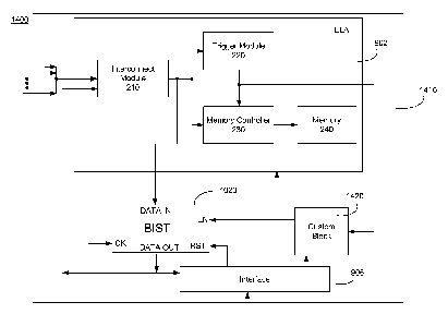
[0057] Fig. 14 is a block diagram of system 1400 according to another
embodiment.
System 1400 may include integrated circuit 1410 having embedded logic analyzer
902 which
may include interconnect module 210, trigger module 220, memory controller 240
and
memory 250 as described above, and receive signals from various system modules
for test or
debug. In addition, integrated circuit 1410 may include BIST block 1020 as
described above
with respect to Fig. 13, having a data input and a data output coupled to
embedded logic
analyzer 902 as well as an enable input. Interface 906 may be coupled to
embedded logic
analyzer 902 and BIST block 1020 for providing user access thereto. In
addition, integrated
circuit 1410 may include a custom block 1420.
[0058] Custom block 1420 may be connected between trigger module 220 of
embedded logic analyzer 902 and BIST block 1020. In particular, custom block
1420 may
include an input coupled to at least one output of trigger module 220, and an
output coupled
to the enable input of BIST block 1020. Custom block 1420 may generate at
least one signal
at its output which is based upon the detection of at least one triggering
event by trigger
module 220.
[0059] Similar to custom block 920, custom block 1420 may include
circuitry that is
specific to the system modules M that are capable of being tested or debugged
by embedded
17
CA 02807323 2013-01-31
WO 2012/033876 PCT/US2011/050761
logic analyzer 902. In one embodiment, the functions performed by custom block
1420 in
generating one or more output signals may be configurable and/or programmable
using
FPGA or CPLD circuitry, a processor executing downloaded test/debug code,
state machine
circuitry, etc. Interface 906 may be coupled to custom block 1420 for
providing access
thereto so that custom block 1420 may be controlled, configured and/or
programmed using a
network device, such as a host device.
[0060] As mentioned, custom block 1420 may receive as an input one or
more signals
generated by trigger module 220. In particular, one or more trigger signals
generated by
trigger module 220, which indicates the detection of at least one event, may
be provided as an
input to custom block 1420. One or more output signals generated by custom
block 1420 and
provided to BIST block 1020 thus may be based upon the one or more trigger
signals
generated by trigger module 220 as well as the functions that are configured
and/or
programmed in custom block 1420. In this way, an output signal generated by
custom block
1420 which selectively enables BIST block 1020 may be defined based upon
signals
generated by system modules M under test or debug as well as actions and
functions that are
defined and executed at runtime of a test or debug session.
[0061] The one or more output signals generated by custom block 1420
that enables
BIST block 1020 may also serve to disable BIST block 1020. Such one or more
signals may
disable BIST block 1020 based upon the detection of one or more trigger events
by trigger
module 220 and/or upon a predetermined function defined in custom block 1420.
The
predetermined function, which may be configured or otherwise programmed at
runtime of a
test or debug session, may including a timer function which disables BIST
block 1020 a
predetermined period of time following its enablement. It is understood,
though, that the
signal which disables BIST block 1020 may be based in part upon virtually any
predetermined function defined in custom block 1420.
[0062] It is further understood that integrated circuits 1010 and 1410
may include
more than one BIST block 1020 so that multiple signatures may be separately
maintained and
generated during a test or debug session. Fig. 15 illustrates a system 1500
having integrated
circuit 1510 which includes multiple BIST blocks 1020 and 1020', each of which
receives
one or more signals from embedded logic analyzer 902. In particular, each BIST
block 1020,
1020' may receive a distinct set of one or more signals from or associated
with embedded
logic analyzer 902, such as signals appearing at the output of interconnect
module 210. The
output of each BIST block 1020, 1020' may be coupled to embedded logic
analyzer 902 for
18
CA 02807323 2013-01-31
WO 2012/033876 PCT/US2011/050761
sampling or storing therein. For example, the data output of each BIST block
1020, 1020'
may be coupled to an input of embedded logic analyzer 902, as shown in Fig.
15.
[0063] Each BIST block 1020, 1020' may be separately enabled and
disabled for
signature generation. In particular, the enable/disable input of each BIST
block 1020 and
1020' may be coupled to the output of a distinct custom block 1420 and 1420',
respectively.
Each custom block 1420, 1420' may receive at an input thereof one or more
signals from
trigger module 220. The one or more signals received from trigger module 220
by each
custom block 1420, 1420' may be distinct relative to the one or more signals
received by the
other custom block 1420, 1420'. In addition, each custom block 1420, 1420' may
be
separately programmed and/or configured by a host device using interface 906.
As a result,
custom blocks 1420 and 1420' may be capable of separately and independently
enabling and
disabling its corresponding BIST block 1020 and 1020', respectively. It is
understood that
system 1500 may include more than two BIST blocks 1020 and 1020' depending
upon the
system modules M to be tested and debugged.
[0064] The operation of systems 1400 and 1500 will be described with
reference to
Figs. 16a and 16b. At runtime of a test or debug session, trigger events are
defined at 1610
for configuring the trigger events that trigger module 200 is to detect during
the session. At
around the same time, the functions performed by custom blocks 1420 and 1420'
are defined
at 1620 so that custom blocks 1420 and 1420' generate enable signals for BIST
blocks 1020
and 1020', respectively, according to desired functions that may be based upon
the particular
system modules M being tested or debugged. This may be accomplished by
programming
programmable circuitry in custom blocks 1420 and 1420'. In the event custom
blocks 1420
and 1420' include a processor, this defining may be accomplished by loading
code into
memory that is accessible by the processor for execution. It is understood
that defining the
functions to be performed by custom blocks 1420 and 1420' depends upon the
particular
implementations of such blocks.
[0065] Also at runtime, each of BIST blocks 1020 and 1020' may be
placed in its
known, predetermined state at 1630 using interface 906. Next, during the
system test or
debug session, at 1640 embedded logic analyzer 902 may receive signals from
one or more
system modules M. During this time, embedded logic analyzer 902 may select at
1650
certain signals from the received signals as candidate signals. This selection
may be
performed by interconnect module 210. One or more of the selected candidate
signals may
be used by trigger module 220 for detecting for the occurrence of a previously
defined trigger
19
CA 02807323 2013-01-31
WO 2012/033876 PCT/US2011/050761
event, while other candidate signals may be available for signal capture in
response to such
detection.
[0066] Next, a determination may be made at 1660 by trigger module 220
whether
one or more previously defined trigger events have occurred. Upon an
affirmative
determination that a trigger event has occurred, one or more candidate signals
may be
captured by memory controller 240 and stored in memory 250. In addition or in
the
alternative, the detection of a trigger event by trigger module 220 may cause,
at least in part,
at least one of custom blocks 1420 and 1420' to generate an enable signal at
1670 for
enabling a corresponding BIST block 1020 and 1020', respectively, depending
upon the
function previously defined at 1620. In the event a custom block 1420 enables
its
corresponding BIST block 1020 at least partly in response to the detection of
a trigger event,
a new signature is generated at 1680 at each clock pulse based upon the
previously
maintained signature and upon the signals appearing at the data input of BIST
block 1020.
[0067] At some point in the test or debug session following detection
of a trigger
event at 1660, another trigger event may occur at 1685 to disable the
previously enabled
BIST block 1020. This trigger event may be detected, for example, by trigger
module 220
based upon one or more of the candidate signals selected at 1650.
Alternatively, such trigger
event may be based upon the lapse of a predetermined period of time following
the
enablement of BIST block 1020 or following the detection of the trigger event
in 1660, as
monitored by trigger module 220 or custom block 1420. Upon the detection of
the trigger
event at 1685, BIST block 1020 may be disabled which thereby inhibits further
signature
generation. At this point, the signature generated by BIST block 1020 may be
provided to
embedded logic analyzer 902 at 1690 for sampling and storage or for event
triggering therein.
The signature may also be provided over interface 906 for analysis.
[0068] If the test or debug session is not complete, operation may resume
at 1660 for
determining whether another trigger event has occurred, or at 1650 for
selecting another
group of signals to serve as candidate signals.
[0069] The generated signature may be provided at 1690 to embedded
logic analyzer
902 for initiating a trigger event or for signal capture by memory controller
240 for storage in
memory 250. This may occur following BIST block 1020 no longer being enabled.
In the
event the generated signature is captured and stored in memory 250, the
signature may be
thereafter retrieved for analysis. Such analysis may include comparing the
retrieved
CA 02807323 2013-01-31
WO 2012/033876 PCT/US2011/050761
signature to an expected signature value identified through system simulation,
and
determining that the system is operating correctly if the retrieved signature
matches the
expected signature value.
[0070] It is understood that any one or more of BIST blocks 1020 and
1020' and
custom blocks 1420 and 1420' may be included within logic analyzer 902. It is
further
understood that integrated circuits 1010, 1410 and 1510 may be used in
virtually any system
which may benefit from an embedded mechanism to facilitate the efficient
testing and
debugging of the system and the system modules M thereof. For example, a
printer, all-in-
one printing device or multifunction printer may include integrated circuit
900.
[0071] A mechanism for testing and debugging a system may include, in
addition to
custom blocks 904 and 920, software to communicate with embedded logic
analyzer 902 and
custom blocks 904 and 920. The software provides the user with the ability to
select in-
system options for such blocks and control or otherwise program them after the
system has
been synthesized and/or assembled, such as at runtime of a system test or
debug session. The
software, including a user interface, provides communication with embedded
logic analyzer
902 and blocks 904 and 920 via interface 906. The software may be used to
receive at a
remote device the data sampled and stored by embedded logic analyzer 902 and
display the
signals to the remote device user.
[0072] It will be apparent to those skilled in the art that various
modifications and
variations can be made to the present invention without departing from the
spirit and scope of
the invention. For example, it is understood that the embedded logic analyzer
902 may
include an output module 230 and controller 270 found in embedded logic
analyzer 200 of
Fig. 2. In addition or in the alternative, integrated circuit 900, 910 and 940
may include a
CPU 500 and storage medium 510 coupled to embedded logic analyzer 902 as shown
in Figs.
5 and 6. Integrated circuits 900, 910 and 940 may also include a processor 710
coupled to
trigger module 220 as shown in Fig. 7. Thus it is intended that the present
invention cover
the modifications and variations of this invention provided they come within
the scope of the
appended claims and their equivalents.
21