Note : Les descriptions sont présentées dans la langue officielle dans laquelle elles ont été soumises.
CA 02810053 2013-03-20
READING DEVICE IN WIRED COMMUNICATION WITH A PROBE
HAVING AN EMBEDDED MEMORY DEVICE
Background of the Invention
Field of the Invention
[0001] The present invention is directed to a monitoring system and method for
operating the
system including a reading device in wired communication with a probe. In
particular, the
present invention is directed to a monitoring system in which the reading
device is in wired
communication with a probe having a memory device embedded therein to prohibit
being
separated from a sensor by the user during use.
Description of Related Art
[0002] Medical probes comprising one or more physiological sensors or
transducers are used
to measure parameters such as, but not limited to, pressure, tension or
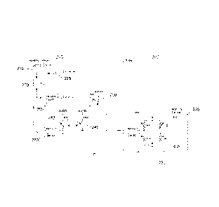
displacement. Such
probes may be external to the body or implantable within the body. Some
sensors or
transducers such as pressure sensors are typically designed as a resistive
bridge balancing
circuit (e.g., a Wheatstone bridge). When using a sensor or transducer a non-
volatile
read/write memory may be required to store data such as calibration parameters
(e.g., zeroing,
temperature coefficient), information associated with a patient (e.g., age)
and/or equipment
information (e.g., probe expiration date, probe usage time and/or failure mode
information
(for instance, recovery data in case of memory corruption)). As an
illustrative example, the
medical probe may be a differential pressure sensor for measuring intracranial
pressure (1CP)
within the brain. In such application, prior to implantation of a device
(e.g., implantable ICP
solid state sensor) an ambient pressure reference value, also referred to as
"zero reference
value" or "offset reference value," is detected and stored in a memory.
Typically, the zero or
offset pressure reference value is measured when the sensor is wet by soaking
the tip in a
shallow pool of sterile water or sterile saline for a predetermined period of
time (e.g.,
approximately 15 minutes to approximately 30 minutes). Alternatively, the zero
or offset
1
CA 02810053 2013-03-20
=
11.
reference value (e.g., offset pressure value) may be measured in air. During
use, each
measurement value detected by the sensor is compensated or offset by the
previously
calibrated offset reference value to produce a compensated value.
[0003] Reading of information from or writing of information to the memory
device
associated with the probe by a separate reading device occurs via a
communication interface
(e.g., wireless or wired). A wireless communication interface using such
technology as bar
code scanning is limited to reading information stored in the memory
associated with the
probe. Writing or storing of new information to the memory device is not
permitted with bar
code scanning. Other commonly used wireless technology such as Radio Frequency
Identification (RFID) disadvantageously increases the overall complexity due
to the
additional circuitry and components required.
[0004] Alternatively, a wired connection via an interface cable may be used to
transmit
information to and from the reading device, wherein the probe and a memory
device are
embedded within the interface cable itself. The zero or offset reference value
stored in
memory must undesirably be reentered/acknowledged whenever interface cables
used to
connect the probe to the reading device are replaced or even when the same
interface cables
are used to reconnect the probe to the reading device. Furthermore, a reusable
interface cable
that requires sterilization, (e.g., autoclaved), may possibly result in
physical damage to the
memory. Thus, embedding of the memory device in the interface cables
disadvantageously
permits the memory device to be separated from the probe itself. For either a
reusable or one-
time-usage probe capable of being powered off or disconnected while in use, it
is preferable
that separation of the memory from the probe by the patient while in use be
prohibited in
order to: (i) avoid the possibility of crossing the probe with a memory
associated with a
different probe and thus avoid the use of wrong data; (ii) retain data stored
within the memory
device even in the absence of power; and (iii) reduce complexity of confirming
the zero value
associated with a probe.
[0005] It is therefore desirable to develop a probe with a memory device
embedded therein
that prohibits separation by the user during use while simultaneously
minimizing the overall
2
CA 02810053 2013-03-20
footprint of the probe and the number of wires/lines/electrical connections
between the probe
and a separate reading device.
Summary of the Invention
[0006] The present invention is directed to a probe with a memory device
embedded therein
that prohibits separation by the user during use while simultaneously
minimizing the overall
footprint of the probe and the number of wires/lines/electrical connections
between the probe
and a separate reading device.
[0007] One aspect of the present invention is directed to a monitoring system
including a
reading device electrically connected to a probe via a wired interface. The
probe has a
physiological sensor/transducer configured as a Wheatstone resistive bridge
balancing circuit.
Integrated within the housing of the probe to prohibit separation during use
by a user is a
memory device arranged in parallel with the sensor. Communication between the
reading
device and the probe occurs via a wired interface utilizing a same number of
electrical
connections between the reading device and the Wheatstone resistive bridge
balancing circuit
as would be required if the memory device was eliminated. Control circuitry
controls
selection between one of two modes for accessing either sensor signal response
or data from
the memory device.
[0008] Another aspect of the present invention relates to a method for
operating the
monitoring system described in the preceding paragraph. Specifically, the
method includes
the step of configuring, via a control signal generated by the control
circuitry, the position of
each switch so as to select between the two modes.
Brief Description of the Drawing
[0009] The foregoing and other features of the present invention will be more
readily apparent
from the following detailed description and drawings of illustrative
embodiments of the
invention wherein like reference numbers refer to similar elements throughout
the several
views and in which:
3
CA 02810053 2013-03-20
I.
[0010] Figure 1 is an exemplary schematic diagram of a prior art monitoring
system
including a reading unit communicating via several wire-lines/connections with
a probe
having a memory device embedded therein;
[0011] Figure 2A is an exemplary schematic diagram of a system in accordance
with the
present invention including a reading device having three switches
communicating via a one-
wire protocol using a One-Wire Master with a probe having a resistive
Wheatstone bridge
and a slave One-Wire memory device embedded therein;
[0012] Figure 2B is an exemplary schematic diagram of another embodiment of a
system in
accordance with the present invention including a reading device having one
switch
communicating via a UNI/O protocol using a UNI/O Master with a probe having a
resistive
Wheatstone bridge and UNUO single I/0 memory device embedded therein and one
switch;
[0013] Figure 2C is an exemplary schematic diagram of yet another system in
accordance
with the present invention including a reading device having one switch
communicating via a
one-wire protocol using a One-Wire Master with a probe having a resistive
Wheatstone
bridge and a slave One-Wire memory device embedded therein;
[0014] Figure 3 is a schematic diagram of the system of Figure 2A wherein the
three switches
in the reading device are set in a sensor access mode in which access is
provided to the
sensor/transducer measurements; and
[0015] Figure 4 is a schematic diagram of the system of Figure 2A wherein the
three switches
in the reading device are set in a memory access mode in which access is
provided for either
writing data to/reading data from the memory device embedded in the probe.
Detailed Description of the Invention
[0016] The present invention discloses a monitoring system including a reading
device (e.g.,
external bedside monitor or neuro-monitor) connected via a wired interface
(e.g., one or more
interface cables) to a probe. The probe includes one or more physiological
sensors or
transducers configured as a Wheatstone resistive bridge balancing circuit.
Embedded,
4
CA 02810053 2013-03-20
included or integrated within the housing of the probe is a memory device such
that the sensor
and memory device are prohibited from being separated from one another during
use by a
user. The memory device is preferably a non-volatile memory device.
[0017] Many different types of memory devices are available of which the
number of
electrical wire-line connections required vary. Figure 1, is a prior art
system wherein four
wires-lines plus an additional k wires-lines (where k 2) electrically connect
electronic control
circuits 115, 125 associated with external reading device 110 (e.g., a neuro
monitor) and
probe 120, respectively. Thus, at a minimum, when k=1, five wires-lines are
required
between the control circuits 115, 125. Electronic control circuitry 125 in
probe 120 is
electrically connected in series with sensor/transducer 130 and a Serial
Peripheral Interface
(SPI) memory device 135. Memory device 135 is accessed by the external reading
device
110 via electronic control circuitry 125. Electronic control circuits 115, 125
connect the
sensor(s)/transducer(s) of probe 120 to the external reading device 110 in
order to access
physiological measurements and/or other data from the sensor(s)/transducer(s).
Electronic
control circuitry 125 employs four wires-lines plus an additional k wires-
lines (where k 2) in
order to connect the sensor/transducer 130 or the memory 135 to the external
reading device
110. In this prior art configuration the additional circuitry (electronic
control circuitry 125)
and k additional wires-lines disadvantageously increase the overall cost and
size of the
footprint and the interface cable section. Even in the case in which
electronic control circuitry
125 is eliminated altogether by electrically connecting circuit 115 directly
to the sensor 130
and memory 135, the additional wire-line electrical connections still increase
the overall cost.
[0018] Alternatively, it is also well known in the art to substitute an I2C
memory device for
the SPI memory device in Figure 1. Despite the number of wires-lines desirably
being
reduced from that of the SPI memory device, the need for additional wire-line
connections
required when using the I2C memory chip relative to that without the embedded
memory
device still increases the overall cost of manufacture and the size of the
probe footprint. The
overall cost of manufacture is always a concern, but with some applications,
most notably,
intracranial pressure, minimizing the footprint size of the probe is a
significant factor in its
design configuration. It is therefore desirable to utilize a design that
minimizes the number of
wire-line connections between the memory device embedded in the probe and the
separate
5
CA 02810053 2013-03-20
external reading device. In particular, for existing products, it is desirable
to embed within
the probe a one-wire memory device in which the number of wires-lines required
is equal to
that without the memory device in the probe.
[0019] Figure 2A is such an exemplary system in accordance with the present
invention
wherein the probe has embedded therein a memory device (i.e., a "one-wire
memory device")
(for example, a One-Wire EEPROM memory device manufactured by Maxim
Integrated
Products, Inc.) requiring only two pins, contacts or electrical wires, i.e.,
one for ground and
the other for the Data/Power supply. In addition, the circuit design or
configuration in
accordance with the present invention permits sharing of common wire-line
connections
thereby utilizing the same number of wires-lines (e.g., four wires-lines, not
including the
shield connection) for interfacing between reading unit 210 and either the
sensor/transducers
230 or the memory device 235 as would be required without the memory device.
Moreover,
the need for additional circuitry (e.g., control circuitry 125 associated with
the probe as shown
in prior art Figure 1) is eliminated and thus the overall size of the
footprint is reduced by
arranging the One-Wire memory device 235 in parallel with the
sensor/transducer 230.
Electronic control circuitry 215 allows external reading device 210 to access
(e.g., reading of
data from/writing data to) the One-Wire non-volatile memory device 235
embedded in the
probe 220. Supply voltage and electronics around the One-Wire memory device
are
designed in such way that the One-Wire device works within manufacturer
specifications
(e.g., I/0 logical level, I/0 current sink, etc.)
[0020] In the system 200 in Figure 2A, external reading device 210 is
electrically connected
to probe 220 via 4 wires-lines. Probe 220 includes an EEPROM memory device
235,
preferably a One-Wire EEPROM memory device such as DS2431 a 1024-bit, one-
wire
EEPROM chip manufactured by Maxim Integrated Products, Inc. Although probe
220, as
depicted in Figure 2A, has only a one-wire memory device, it is contemplated
and within the
intended scope of the present invention to include additional one-wire devices
such as, but not
limited to, a DS18S20 One-Wire Digital Thermometer manufactured by Maxim
Integrated
Products, Inc., arranged in parallel with the one-wire memory device 235. The
one-wire
memory device may be selected to also include an additional digital port,
wherein the digital
signals received via the port may specifically configure the sensor, for
example, during a self-
6
CA 02810053 2013-03-20
test or a calibration. One such additional digital port may be provided using
a DS28E04-100,
4096-bit, One-Wire EEPROM chip manufactured by Maxim Integrated Products
having
two general-purpose I/0 ports that can be used for input or to generate level
and/or pulse
outputs. Electronically connected to the One-Wire EEPROM 235 is a
sensor/transducer
230, for example, a Wheatstone resistive bridge balancing circuit (without
Kelvin connections
in this example) having two excitation lines (Vs+, Vs-) and two differential
output voltage
lines (sensor+, sensor-). As stress is applied to the strain gauge, a change
in resistance
unbalances the Wheatstone bridge resulting in a signal output (sensor+, sensor-
), related to the
stress value. Since the differential signal output value is relatively small,
(typically a few
hundred microvolts) a differential amplifier or instrumentation amplifier 270
is preferably
employed to boost or increase the sensor output signal level to a full scale
of preferably,
approximately 2.5V volts around bias voltage (e.g. using a gain of preferably
approximately
128). Amplifier 270 is a separate device. It is, however, contemplated for the
amplifier to be
embedded within an analog-to-digital converter (ADC) such as ADS1246
manufactured by
Texas Instrument. Additional signal conditioning electronics may be employed
to further
process the sensor output signals.
[0021] Three switches SW1, SW2, SW3 (referred to by reference element numbers
240, 245,
250, respectively) are utilized to set or control probe 220 between one of two
modes,
configurations or states. Each of the switches may be analog switches, solid
state relays,
transistors (e.g., a P-channel MOSFET switch), photo-transistors or any
combination thereof.
For instance, switches SW1, SW2 may be two single pole, single throw (SPST)
switches
SW1, SW2 while switch SW3 is one single pole, double throw (SPDT) switch. As
an
alternative configuration, the one SPDT switch SW3 may be realized by using
two SPST
switches. A first memory access mode, configuration or state is one in which
memory device
235 is accessible by the reading device 210 for reading and/or writing
operations. In a second
sensor access mode, configuration or state the data (e.g., physiological
parameter values)
detected by the sensor/transducer 230 is accessible by the reading device 210.
[0022] Electronic control circuitry 215 associated with the external reading
device 210 is
used to configure or control the settings of each of the switches SW1, SW2,
SW3 and thus
select between the two different modes. In order to access the memory device
235 to perform
'7
CA 02810053 2013-03-20
reading/writing operations, control circuitry 215 preferably includes a One-
Wire Master 255
manufactured by Maxim Integrated Products, Inc. that provides data, signaling
and power via
a single signal serial clock, data input/output (SCIO) pin. This type of one-
wire interface or
bus requires only two wires: data and ground. The One-Wire Master may be
realized either
by a software layer or by means of a hardware module such as a UART to One-
wire
converter; an I2C to a One-wire converter (e.g. DS2482/DS2483 from Maxim
Integrated
Products, Inc.); a USB to One-wire converter; or it may be synthesized into an
ASIC/FPGA.
In addition, control circuitry 215 also includes a CPU 260 such as a
microcontroller, a FPGA,
a processor, a programmable logic and/or a combination of any of these
devices. The output
of the control circuitry 215 generated by I/O block 265 is a control signal
(SW_ON/OFF) for
configuring the settings of each of switches SW1 and SW2. Analog signal supply
voltage
AVDD supplies the sensor/transducer excitation voltage reference and
alternately the power
necessary for reading data from/writing data to the memory.
[0023] In operation, as depicted in Figure 4, when the reading device seeks
access to (i.e.,
write data to or read data from) the memory device 235, the control signal
output
(SW ON/OFF) generated by the control circuit 215 sets the orientation of each
of switches
SW1 and SW2 to enable a first mode or Memory Access Mode. In this first mode,
SW1 240
and SW2 245 are connected to the excitation power supply voltage (AVDD) (e.g.,
5V), while
switch SW3 250 is configured to connect the control circuit 215 of the reading
device 210 to
the memory device 235. While in this first mode, configuration or state, the
excitation power
supply voltage AVDD is not applied to the sensor/transducer 230. Instead,
resistors R1 and
R2 of the Wheatstone bridge 230 connected via the 1/0 line of the One-Wire
memory
device 235 act as a pull-up resistor pulling up the cun-ent to Vs+ (e.g., 5V).
Without such
pull-up resistance the data could neither be written to nor read from the
memory device 235.
It is worthwhile noting that an external pull-up resistor separate from or in
addition to those in
the Wheatstone bridge may not alternatively be employed to provide the
necessary pull-up
resistance. The reason being that resistors R3 and R4 connected to ground pull-
down and
thus defeat or cancel out the functionality provided by such separate or
additional external
pull-up resistance.
8
CA 02810053 2013-03-20
=
[0024] A second mode or Sensor Access Mode in which the sensor/transducer
output signal
of the probe is accessible by reading device 210 is enabled by setting
switches SW1 and SW2
so that they are not powered by the excitation power supply voltage AVDD,
while switch
SW3 connects the excitation power supply voltage AVDD to the memory device
235, as
illustrated in Figure 3. In this second configuration or state, power signal
AVDD (e.g.,
approximately 5 V) is supplied to the Wheatstone bridge 230, while the memory
device 235 is
placed in standby mode so as not to interfere with the sensor/transducer
signals.
[0025] Both switches SW1 and SW2 are preferably chosen so that their leakage
current does
not impact the quality of the measured sensor signals, while the switch SW3 is
preferably
chosen with a low on resistance (RON) in such a way that it does not impact
the quality of the
measured sensor signals.
[0026] As an alternative, if the impedance of the transducer bridge 230 is
relatively high
(e.g., approximately 2000 ohms or greater), the bridge may be connected in
parallel to the
memory device 235 while accessing the memory, during which time the bridge
acts as a
relatively weak pull down resistor (as shown in Figure 2C). Power to the
memory device is
supplied via a digital voltage DVDD (e.g., approximately +5V) This alternative
embodiment
advantageously eliminates the need for switches SW1 and SW2 wherein switching
between
the sensor and memory access modes is realized using a single switch SW3 250;
however,
such configuration is limited to transducer bridges having a relatively high
resistance
approximately 2000 ohms and greater.
[0027] Figure 2B is an exemplary schematic diagram of an alternative
embodiment in
accordance with the present invention employing a UNI/08 single I/0 EEPROM
235'
manufactured by Microchip and a single switch SW3 250. Communication between
the
reading device and probe is via a UN1/08 Master 255'. Such configuration
requires
additional circuitry inside the probe. Specifically, a capacitor Cl and a
Schottky diode D1
together act as a rectifier 275 to insure that the voltage supply does not
fall below the minimal
supply voltage level during the data transfer between the reading device 210
and the memory
device 235. The capacitor Cl is preferably non-polarized.
9
CA 02810053 2013-03-20
[0028] Thus, the present inventive circuit configuration advantageously
eliminates the need
for additional lines/wires/electrical connections between a reading device and
a probe when
embedding a memory device (e.g., One-Wire memory device or UNI/0 single I/O
memory device in the probe). Although the present claimed invention has been
shown and
described with respect to only a One-Wire memory device or UNI/08 memory
device
embedded in the probe, additional one-wire devices may also be embedded
therein. By way
of example, a DS18S20 One-Wire digital temperature sensor manufactured by
Maxim
Integrated Products, Inc. may be connected in parallel with the memory device.
Furthermore,
minimal additional space is required for embedding the memory device in the
probe, requiring
the addition of only one chip (i.e., the memory device itself). The need for
separate or
additional pull-up resistance(s) may be eliminated, in accordance with the
embodiment in
Figure 2A of the present invention, wherein pull-up resistance necessary for
the memory
functionality is instead uniquely provided by the Wheatstone bridge. The
present inventive
configuration realizes the aforementioned advantages by employing circuitry
for selecting
between two dedicated modes, configurations or states: (i) a first mode or
Sensor Access
Mode permits access to the sensor(s) measured signal by the reading device,
without the
memory altering the sensor(s) signal quality; and (ii) a second mode or Memory
Access Mode
allowing the reading of data from and/or the writing of data to the memory
device embedded
in the probe.
[0029] Thus, while there have been shown, described, and pointed out
fundamental novel
features of the invention as applied to a preferred embodiment thereof, it
will be understood
that various omissions, substitutions, and changes in the form and details of
the devices
illustrated, and in their operation, may be made by those skilled in the art
without departing
from the spirit and scope of the invention. For example, it is expressly
intended that all
combinations of those elements and/or steps that perform substantially the
same function, in
substantially the same way, to achieve the same results be within the scope of
the invention.
Substitutions of elements from one described embodiment to another are also
fully intended
and contemplated. It is also to be understood that the drawings are not
necessarily drawn to
scale, but that they are merely conceptual in nature. It is the intention,
therefore, to be limited
only as indicated by the scope of the claims appended hereto.