Note : Les descriptions sont présentées dans la langue officielle dans laquelle elles ont été soumises.
CA 02810827 2013-03-07
WO 2011/066028
PCT/US2010/047977
- 1 -
WIRELESS PASSIVE RADIO-FREQUENCY STRAIN AND DISPLACEMENT
SENSORS
RELATED APPLICATION
This application claims the benefit of U.S. Provisional Application No.
61/240,430, filed September 8, 2009, the entire teachings of which are
incorporated
herein by reference.
GOVERNMENT SUPPORT
The invention was supported, in whole or in part, by an Award No. W911NF-
07-2-0081 from the Army Research Laboratory. The Government has certain rights
in the invention.
BACKGROUND OF THE INVENTION
Structural health monitoring to assess the integrity of civil infrastructure,
aerospace components, and military aircraft components is critical for the
estimation
of the optimal service life of these structures and prevention of catastrophic
failure.
Crack and strain sensing are some of the aspects of structural health
monitoring.
Catastrophic failure may be caused by strains or displacement beyond allowable
(or
design permitted) levels, and failure is often preceded by the formation of
cracks that
are caused by strain.
Strain sensing is one of the most critical aspects of structural health
monitoring and non-destructive evaluation. There is a demand for robust strain
and
displacement sensors that are light-weight, cost-effective, and easy to
install. Strain
sensors that can measure considerable strains over large areas of structures
are
needed. Traditional resistive metal foil strain gauge sensors, though low-cost
and easy
to install, have limitations, such as the need for a physical connection of
the sensing
element with the interrogation unit. Fiber-optic-based sensors have also
received
considerable attention since they are very compact and can provide very high
resolution. However, they have inherent problems such as fragility and
susceptibility
WO 2011/066028 CA 02810827 2013-03-07
PCT/US2010/047977
- 2 -
to damage. In both these types of strain sensors, the physical connection
between the
sensor and the interrogation unit is also prone to corrosion and fracture. In
addition,
wireless monitoring of strains in the absence of a clear line of sight and/or
physical
connection to the structure of interest is impossible using conventional
resistive or
capacitive strain gauges. Conventional strain gauges often have active
elements that
deform when a load is applied. The performance of these strain sensors tend to
deteriorate/drift over time since the fatigue life and mechanical properties
of the
metallic element determines the ultimate performance.
Recently, wireless sensors have been the subject of tremendous interest. U.S.
Patent Application Publication No. 2007/0186677 Al, incorporated by reference
herein in its entirety, discloses a non-contact radio-frequency (RF) strain
sensor that
uses a planar LC (inductor-capacitor combination) circuit element for
detecting the
resonant frequency change caused by structural deformation proportional to the
applied stress. However, this strain sensor contains metallic sensing elements
that
physically deform on application of the load. The long-term performance of
these
strain gauges again depends on the fatigue life of the metallic sensing
elements, which
can typically undergo only a few thousands to tens of thousands of cycles
before
failure or deterioration in performance. Unfortunately, strain sensors with
deformable
metallic sensing elements may fail too soon to be suitable for long-term
sensing
applications, such as monitoring bridges, towers, aircraft components, and the
like. In
addition, premature failure of deformable metallic sensing elements may not be
distinguishable from failure of the structure being monitored.
SUMMARY OF THE INVENTION
Embodiments of the present invention include multi-layer strain sensors,
methods of sensing strain, and methods of making multi-layer strain sensors.
Example strain sensors include first and second sensing layers formed on first
and
second rigid substrates, respectively. The sensing layers are separated by an
insulating interlayer, which can a flexible elastomer or other suitable
material,
including air. The sensing layers are coupled together electromagnetically
(i.e.,
capacitively and/or inductively) to form a structure that resonates at a
resonance
frequency that depends on the relative displacement between the first and
second
WO 2011/066028 CA 02810827 2013-03-07
PCT/US2010/047977
- 3 -
sensing layers. Transmitting a radio frequency (RF) signal toward the sensor
produces transmitted and reflected RF signals that each show a peak at the
resonance
frequency. Moving the first sensing layer with respect to the second sensing
layer
causes the resonance frequency to shift, causing the peak in the transmitted
and
reflected RF signals to shift.
Strain sensors of the invention typically have much longer fatigue lives than
conventional sensors because the rigid substrates employed in the invention
inhibit
defolination of the sensing elements during application of a tensile or
compressive
load to the sensor. Instead, tensile and compressive loads cause the to
interlayer to
defolin. Unlike the sensing layers, which are typically metallic, the
interlayer can be
made of an elastomer or other insulating material capable of undergoing
millions of
deformation cycles before failure. Some sensors may even have air interlayers.
As a
result, the sensors disclosed herein are more suitable for measuring stress
and strain in
bridges, buildings, aircraft, etc. than conventional strain sensors.
BRIEF DESCRIPTION OF THE DRAWINGS
The claimed concepts will be apparent from the following more particular
description of example embodiments of the invention, as illustrated in the
accompanying drawings in which like reference characters refer to the same
parts
throughout the different views. The drawings are not necessarily to scale,
emphasis
instead being placed upon illustrating embodiments of the present invention.
FIG. lA is a schematic diagram of a multi-layer strain sensor of the
invention.
FIG. 1B is a schematic diagram of the multi-layer strain sensor of FIG. lA
attached to a test sample.
FIGS. 2A and 2B are schematic views of a strain/displacement sensor and a
strain/displacement sensor attached to a test sample, respectively.
FIGS. 3A-3D show plan views of sensing elements suitable for use in upper
and lower sensing layers.
FIG. 4 is diagram of a wireless interrogation system suitable for probing a
multi-layer strain sensor.
FIG. 5 is a plot of RF response of the multi-layer strain sensor of FIG. 1
under
tensile strain.
WO 2011/066028 CA 02810827 2013-03-07
PCT/US2010/047977
- 4 -
FIG. 6 is a plot of resonant frequency versus percent tensile strain for the
sensor of FIG. 1.
FIG. 7 is a plot of resonant frequency versus percent compressive strain for
the
sensor of FIG. 1.
FIG. 8 is a plot of resonance frequency and tensile stress versus percent
strain
for a multi-layer strain sensor with a polypropylene (PP) sample.
FIG. 9A is a plot of frequency response from a printed LC sensor and a
cracked sensor
FIG. 9B is an optical micrograph of a microcrack propagating through a
printed circuit line.
FIG. 10 is a plan view of a directional sensor that includes five of the
inductor-
capacitor circuits shown in FIG. 7A. Sensor LC0 is disposed above sensors LC1,
LC2,
LC3, and LC4.
FIG. 11 is a plot of resonance frequency for sensors LC1, LC2, LC3, and LC4
versus displacement of sensor LC0 along the 45 axis shown in FIG. 10.
FIG. 12 is a plot of resonance frequency for sensors LC1, LC2, LC3, and LC4
versus displacement of sensor LC0 along the X axis shown in FIG. 10.
FIG. 13 is a plot of resonance frequency for sensors LC1, LC2, LC3, and LC4
versus displacement of sensor LC0 along the Y axis shown in FIG. 10.
DETAILED DESCRIPTION OF THE INVENTION
A description of example embodiments of the invention is as follows.
A multi-layer strain sensor of the invention includes passive RF-responsive
antennas, or sensing elements, that are mounted on rigid (i.e., stiff and
inflexible)
substrates. Displacement of the sensing elements shifts the sensor's resonance
frequency by an amount proportional to the applied strain. The rigid
substrates
prevent the sensing elements from deforming under the applied strain, making
it
possible for the sensor to undergo millions of measurement cycles before
failure. As
a result, the strain sensor is eminently suitable for monitoring strain in
bridges,
buildings, aircraft, and other structures. In some cases, the sensor make be
formed
using the structure itself. For example, the sensing elements can be printed
on
opposing surfaces of the structure under test, with an air or elastomer
interlayer
WO 2011/066028 CA 02810827 2013-03-07
PCT/US2010/047977
- 5 -
separating the sensing elements. Strain on the structure under test causes one
or both
of the surfaces to move (without deforming the sensing elements), resulting in
a
measurable change in the resonance frequency of the circuit formed by the
sensing
elements.
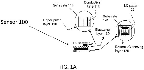
FIG. lA shows an example of an inductively coupled strain sensor 100 that
can detect structural deformation by relative displacement between sensing
elements.
Strain sensor 100 includes an upper sensing layer 102, also known as an upper
patch
layer 102; an insulating interlayer 104 made of polyethylene terephthalate
(PET), an
elastomer, such as silicone fluoropolymer, or another suitable material with a
low
coefficient of friction; and a bottom sensing layer 106, Upper sensing layer
110
includes a conductive line 112 and a rigid substrate 114; similarly, the lower
sensing
layer 120 includes an LC pattern 122 and a rigid substrate 124. Rigid
substrates 114
and 124 can be made of glass, ceramics, thermoset Bakelite, composite
materials,
wood, cement, concrete, or any other suitably rigid material.
Sensing layers 110 and 120 include metallic sensing elements (i.e., conductive
line 112 and LC pattern 122) that are electromagnetically coupled together to
form an
inductor/capacitor (LC) circuit that resonates at radio frequencies, i.e.,
from a few
kilohertz to about 300 GHz. In addition, each sensing element may be RF-
responsive
by itself The RF resonant frequency (fr) of strain sensor 100 is given by
fr = \ 2/ LC1
where L is the inductance and C is capacitance of a resonant circuit formed by
sensing
elements 112 and 122. Movement of upper sensing element 112 with respect to
lower
sensing element 122 changes the inductance (L) and/or capacitance (C) of the
resonant circuit, which affects the value of the resonant frequency according
to the
above equation. Changes in resonant frequency can be monitored by
interrogating the
circuit with a wireless radio-frequency (RF) signal and measuring the
reflected or
transmitted signal from the sensor, as described below with respect to FIG. 7.
FIG. 1B shows sensor 100 of FIG. lA mounted with support arms 140 on a
test substrate 150, which can be subject to a tensile or compressive load.
(Alternatively, lower sensing layer 120 of sensor 100 can be mounted directly
to test
substrate 150, or the strain can be applied directly to rigid substrates 110
and 120.)
WO 2011/066028 CA 02810827 2013-03-07
PCT/US2010/047977
- 6 -
Compressing or stretching test substrate 150 causes upper sensing layer 110 to
move
with respect to lower sensing layer 120 by an amount proportional to the
applied
strain. (Applying a strain to sensor 100 causes interlayer 130 to deform,
allowing
sensing elements 112 and 122 to move without being deformed.) This movement
shifts the resonance frequency by an amount proportional to the change in
inductance
and/or capacitance, which is proportional to the amount of movement.
Interrogating
sensor 100 with a swept RF signal yields a reflected signal with a resonant
absorption
peak whose center frequency shifts as a function of the magnitude of the
applied
strain.
Applying too much strain to test substrate 150 may cause test substrate 150 to
crack and fail. If the crack runs through one or both of sensing layers 110
and 120,
the crack will affect the resonance characteristics of sensor 100. In some
cases, the
resonance frequency of sensor 100 will shift outside the bandwidth or
disappear of the
chirped RF signal used to interrogate sensor 100, leading to the absence of a
resonant
peak in the reflected signal. This absence can be used to indicate the
presence of a
crack in the test structure.
FIGS. 2A and 2B show an alternative strain sensor 200 that includes two
sensing elements, or LC patterns 212, that are sandwiched between opposite
sides of
an insulating layer 230 and two glass substrates 214. Upper and lower LC
patterns
212 may be the same or different, depending on the application, and can be
printed on
the glass substrates 214 as described below. Insulating layer 230, which can
be an
elastomer, plastic film, air, or other suitable material, prevents abrasions
of the printed
sensing elements (LC patterns 212) and electrical contact between the sensing
layers.
Strain sensor 200 is mounted on a test sample 250 (on which the strain has to
be
determined) with the help of support blocks 242 on support arms 240 that
prevent
movement of strain sensor 200 in the Z-direction. Rubber sheets 246 are
secured
between support blocks 242 with adhesives 244.
Applying a force 252 to support arms 240 (e.g., by applying a tensile load to
test sample 250) causes insulating interlayer 230 to deform, which in turn
causes LC
patterns 212 to move with respect to each other. As in sensor 100 of FIG. 1,
glass
substrates 214 prevent LC patterns 212 from deforming during application of
force
252. The displacement between LC patterns 212 causes a shift in the resonance
WO 2011/066028 CA 02810827 2013-03-07
PCT/US2010/047977
- 7 -
frequency of the sensor proportional to the magnitude of applied force 252 as
described above.
One difference between strain sensors 100 and 200 shown in FIGS. 1 and 2,
respectively, and other strain gauges is that the sensing elements (e.g., LC
patterns
212) do not deform to produce a change in resonance frequency. Instead, the
rigid
substrates (e.g., glass substrates 214) inhibit or prevent deformation of the
sensing
elements while the interlayer (e.g., insulating interlayer 230) deforms during
application of a tensile or compressive load aligned in the plane of the test
sample.
The relative movement of the sensing elements with respect to each other
creates a
response (signal) proportional to the movement (strain) that can be monitored
wirelessly, without the requirement for a clear line of sight.
In sensors 100 and 200 shown in FIGS. lA and 2A, respectively, the
individual sensing elements may or may not resonate individually in response
to the
RF signal. Instead, the combination of the top and bottom sensing elements
provides
a resonant response that can be monitored remotely. For example, either the
first
and/or second element can resonate in response to an RF pulse by itself. The
presence
of the other element (e.g., the second element) changes the net resonance
response,
possibly by causing a new resonant peak to supplant the resonant peaks of the
individual sensing elements. After the strain/displacement sensor has been
assembled, the change in the net RF response is proportional to the applied
displacement/ strain.
FIGS. 3A-3D shows designs of suitable LC circuitry (sensing elements). The
sensing elements can include, but are not limited to combinations of the
designs
shown in FIGS. 3A-3D. Those skilled in the art will appreciate that other
designs fall
within the scope of the present invention. For example, other suitable
inductor-
capacitor (LC) combinations may have different combinations of patterns, each
of can
be varied by changing the size and number of inductor turns, and the size,
design, and
number of interdigitated fingers of the capacitor. The actual resonant
frequency of the
sensing device can be varied by variations in the design of the inductor and
capacitor,
variations in the position of the sensing elements, the area of overlap of the
top and
bottom conductive layers, and the thickness and dielectric constant of the
substrates
and the interlayer. Further variations in shape, size, position, and
orientation of the
WO 2011/066028 CA 02810827 2013-03-07
PCT/US2010/047977
- 8 -
sensing elements also fall within the scope of the present invention, as is
clear to those
skilled in the art. When the substrate (or interlayer) is deformed or when
there is
relative movement between the sensing elements, the LC coupling of conductive
layers changes proportionally to the deformation. In turn, the resonant
frequency of
strain sensor changes predictably with the deformation.
Example sensing elements, including those illustrated in FIGS. 3A-3D, may
be printed conductive elements in the sensing layer. These printed elements
may
include, but are not limited to combinations of inductors and capacitors
(i.e., LC
circuits). The inductor(s) and capacitor(s) can be on the same layer or in
different
layers of the sensing structure. They may be coupled inductively or by a
physical
electrical connection. The resonant frequency of strain sensor can be varied
by the
geometric arrangement of upper and bottom conductive elements in the sensor.
Example wireless strain/displacement sensors can be attached to monitor
strain on a variety of substrates that include but not limited to plastics,
ceramics, and
composite materials. Example sensors can also be used to measure displacement
or
crack enlargement in civil structures (e.g., the sensor can be attached across
the
crack). In addition, arrays of wireless sensors can be arranged in particular
geometric
arrangements to detect the direction of displacement and/or the direction of
applied
stress/compression as described below.
Fabrication of Passive Wireless Sensors
Low-cost fabrication of passive wireless sensors for damage detection is a
very promising aspect for structural health monitoring. Currently, the
fabrication of
sensors relies heavily on conventional photolithography which is an extremely
cumbersome and time-consuming process. Recently, a direct-write thermal spray
process combined with ultrafast laser micromachining has been described as an
alternative approach to the fabrication of sensors for wireless strain
monitoring.
However, this is a subtractive process that can involve long machining times
depending on the thickness of the thermally sprayed coatings. Additive
printing
techniques like screen and inkjet printing have emerged as attractive
alternatives to
photolithography due to their simplicity and cost effectiveness.
WO 2011/066028 CA 02810827 2013-03-07
PCT/US2010/047977
- 9 -
Screen printing is particularly suited for the deposition of thick film
circuits
and lends itself to large area, high volume production of patterns on a
variety of
substrates. Line widths of the order of 100 vim can be achieved by screen
printing and
the thickness of the deposited lines after curing, or sintering is about 10
m. Here,
example wireless LC sensors have been fabricated by screen printing for
applications
in sensors that can be used for damage detection. Conductive silver inks have
been
specifically developed for this purpose. These inks can be screen printed and
thermally cured to produce the sensing LC circuits. Conductive inks and pastes
used
in screen printing are generally viscous formulations that are composed of a
functional phase (metal particles and flakes) dispersed in an organic medium
(binders
and solvents). The inks used in this work are cured at temperatures around 150
C.
The method of fabrication of the sensing elements may include but no limited
to
screen printing. The sensing element can be fabricated by any additive process
such
as inkj et, gravure or any other conventional printing method or subtractive
processes
such as laser machining or stamping out from continuous sheets of metal.
The wireless sensors disclosed herein can be fabricated by simple techniques
such as screen-printing using specially formulated conductive silver inks.
Printed
silver ink that can be thermally converted into conductive patterns is used to
screen-
print inductor-interdigital capacitor circuits (LC sensors). These sensors can
be
printed on any substrate (ceramic, glass or even polymeric films) that needs
to be
monitored. Further details of conductive inks can be found in U.S. Provisional
Application No. 61/200,542, filed on Decemeber 1,2008, by Nagarajan et al.,
which
is incorporated by reference herein in its entirety.
Interrogation of Passive Wireless Sensors
FIG. 4 is a schematic diagram of a set-up 400 used to wirelessly interrogate
sensors such as those shown in FIGS. 1 and 2. As described above, the
inductance of
the planar spiral inductor (L) and the capacitance of the interdigital
capacitor (C)
depend on the size and shape of the circuit(s) printed on the sensor. A
Hewlett-
Packard 8 8753C vector network analyzer 402 connected to a loop antenna 404
inductively powers the sensor 100 under test. Making a reflection (S11) or
transmission (S12) measurement with vector network analyzer 402 when sensor
100
WO 2011/066028 CA 02810827 2013-03-07
PCT/US2010/047977
- 10 -
enters the interrogation zone of antenna 404 yields a dip at the resonant
frequency of
LC circuit 100 in the printed sensor. A computer 408 coupled vector network
analyzer 402 via a general-purpose instrument bus (GPIB) interface 406 records
the
measurement for subsequent analysis.
EXEMPLIFICATION
Example 1: Tensile and Compressive Load Measurement
Interdigital capacitance and meander inductance patterns were prepared
by screen printing technology as described above to form upper and lower
sensing layers. The size of LC pattern (lower layer) is 40 mm x 40 mm, and
line
pattern of upper patch layer 30 mm >< 3 mm. An adhesive elastomer layer was
inserted between the two conductive layers as shown in FIGS. 1A and 2A to
create the sensor. The RF response of strain sensors was measured using a
vector
network analyzer in reflection mode (i.e., an S11 measurement). The vector
network
analyzer transmitted a swept RF signal to the strain sensor, which absorbed
the
incident RF signal at a resonance whose center frequency varied with the
applied
load.
FIG. 5 shows a plot of resonant frequency shift caused by a tensile load
applied to a strain sensor similar to sensor 100 of FIG. 1. Alternating solid,
dashed,
and dotted lines show that the absorption resonance (a valley with an
amplitude of
about ¨5.0 dB) shifts from about 93.1 MHz to about 94.4 MHz as the applied
tensile
load increases from 0% to 2.0 %. In this case the resonant frequency shift
changes
linearly with the strain; the shift is on the order of 0.65 MHz/strain %, as
shown in
FIG. 6.
FIG. 7 shows a plot of shift in resonant frequency of a strain sensor
subjected
to compression. Exerting a compressive strain on the sensor causes the center
frequency of the absorption resonance to decrease linearly from about 90.5 MHz
to
about 89.2 MHz. Linearity in tension and compression indicates that the sensor
operates relatively free of hysteresis.
FIG. 8 is a plot of resonance frequency (lines RF1 through RF4) and tensile
stress (lines TS1 through TS4) versus percent strain for four separate
measurements.
Tensile stress varies in a perfectly linear fashion as a function of percent
strain.
WO 2011/066028 CA 02810827 2013-03-07PCT/US2010/047977
-11 -
Resonance frequency is slightly nonlinear due to imperfections in the sensor
and the
material responses of the test substrate and the glue used to secure the
sensor to the
test substrate.
Those skilled in the art will appreciate that the sensor can also be designed
and
manufactured to respond nonlinearly to applied strain. In addition, the rate
and total
amount of shift in resonant frequency can be set depending on the particular
application or measurement.
Example 2: Cracked Sensor Interrogation
Detection of cracks and structural damage in the absence of clear line of
sight
detection is still an important challenge. Fortunately, the RF-based
measurements
described herein can be applied to the detection of cracks in various
structures,
including ceramic plates used in body armor. Structural damage, such as a
crack on a
ceramic plate, leads to a detectable change in the RF response. The ultimate
sensitivity of the measured RF response is determined by the size of the metal
flake
present in the silver ink used for the fabrication of the sensor. The success
of these
sensors ultimately depends on their performance and ease of manufacture.
Most RF-based inductor-capacitor (LC) resonant sensors reported to date are
fabricated using techniques such as photolithography, inkjet printing, thermal
spray,
and laser micromachining. In this example, a sensor was created using the
screen-
printing techniques described above. Conductive silver inks were prepared by
blending silver powder, flakes and silver acetylacetonate in dry form,
followed by the
addition of a-terpineol as the solvent and additional mixing. Homogeneous
viscous
pastes containing about 80% solids were obtained by bead milling the admixed
constituents. The cure temperatures of the foimulated inks were determined
from the
thermal decomposition characteristics of the inks. Theimogravimetric analysis
was
performed on a TA Instruments Q50 thermogravimetric analyzer. The ink
samples
were heated in a nitrogen atmosphere at 10 C/minute up to 600 C.
A printed sensor was made with the inductor-interdigital capacitor circuit
pattern shown in FIG. 3B by screen-printing ink on ceramic substrates using a
305-
mesh monofilament polyester screen and subsequently curing the printed
substrate at
140 C for 15 minutes. The conductive silver inks formulated for screen
printing of
WO 2011/066028 CA 02810827 2013-03-07
PCT/US2010/047977
- 12 -
LC circuits include silver flakes as the predominant functional particles and
an
organic precursor of silver dispersed in a solvent medium. On heating,
evaporation of
solvent occurs while the organic precursor undergoes thermal decomposition to
form
a silver layer. The printed pattern starts becoming electrically conductive at
this stage
and subsequent sintering, leads to the formation of continuous, highly
conductive
traces in the desired pattern, e.g., the pattern of FIG. 3B.
FIG. 9A shows that a sharp resonance (solid line) appears at 107 MHz when
the printed sensor was brought into the interrogation zone of loop antenna 404
shown
in FIG. 4. The observed frequency response was very close to the value of the
resonance frequency obtained by high frequency structural simulator (HFSS)
simulation. The LC resonator in the printed sensor is activated by the
oscillating
electromagnetic field radiated by loop antenna 404 according to Faraday's Law;
this
induces an electromotive force (emf) (Vi) in the planar inductor coils of the
sensor.
The impedance of antenna 404, expressed in terms of the LC parameters, changes
due
to the back emf (Vf) from the printed sensor. The reflected voltage measured
across
loop antenna 404 in is given by:
811= ¨20 logVf¨
At resonance, both the induced emf and the back emf across loop antenna 404
reach a
maximum which is seen as a sharp dip at the sensor's resonant frequency.
FIG. 9B shows an optical micrograph of a crack across a silver line that forms
one of the conductive traces printed on a particular sensor. A microcrack such
as the
one shown in FIG. 9B produces a discontinuity in the sensing elements, thus
disrupting the LC circuit. This is manifested as a loss of the resonant
frequency of the
sensor, indicating the presence of a crack in the substrate. The dashed line
in FIG. 8
shows that interrogating a cracked sensor with the loop antenna yields a
reflection
measurement without a resonant frequency dip. Any form of structural damage
either
leading to the complete disruption of the sensing elements or a change in the
circuit
parameters leads to a detectable change in the resonant characteristics of the
sensor.
This methodology of using printed circuits can be extended to the detection of
structural damage in large-area structures and components.
WO 2011/066028 CA 02810827 2013-03-07 PCT/US2010/047977
- 13 -
Example 3: Passive Wireless Sensor Arrays
Sensors and sensing elements may also be arranged in periodic or aperiodic
arrays. In addition, different sensors and sensing elements in the array(s)
may be
oriented in different directions, depending on the application. Because the
individual
sensors are displaced from each other and/or oriented in different directions,
each
sensor measures a projection of the applied displacement along a different
basis (set
of axes). These measurements can be used to trace the direction of
displacement or
applied strain by measuring the change in resonant frequency profile of each
of the
sensors caused by the relative displacement of the sensing element on
complementary
layers.
FIG. 10 shows an example sensor 900 with four sensing elements 902a-902d
(LC1, LC2, LC3, and LC4) printed on a single surface to formed a single
sensing layer.
Another sensing element 904 (LC0) was printed on an upper surface to form a
complementary sensing layer. The upper sensing element 904 formed pairwise
combinations with each of the sensing elements 902a-902d on the lower sensing
layer, i.e, 902a with 904,902b with 904, and so on, that resonated at slightly
different
nominal center frequencies. Because the resonant frequency of each pairwise
combination is different, the sensor can be used to measure the magnitude and
direction of an applied strain.
The sensor 900 was interrogated with a loop antenna 920 while being subject
to tensile strain along the X, Y, and 45-degree axes shown in FIG. 10, and the
change
in RF response was measured with vector network analyzer 404 coupled to
antenna
400 (FIG. 4). Strain caused the upper sensing element 904 to move with respect
to
the lower sensing layer, yielding changes in the resonance frequencies of the
pairwise
combinations as shown in FIGS. 11-13, which are plots of resonance frequency
versus displacement along the X, Y, and 45-degree axes. By comparing with the
resonant frequency responses of sensing elements, the direction of tensile
strain can
be traced out in FIGS. 11-13. FIG. 11 shows that a 60 mm displacement along
the
45-degree axis caused the center frequencies associated with sensing elements
902a
(LC1) and 902c (LC3) to shift down and up, respectively, by about 15 MHz each.
Similarly, FIG. 12 shows that a 25 mm displacement along the X axis causes the
resonance frequencies associated with sensing elements 902b (LC2) and 902d
(LC4) to
WO 2011/066028 CA 02810827 2013-03-07
PCT/US2010/047977
- 14 -
shift up by about 15 MHz each. The resonance frequencies associated with
sensing
elements 902a and 902c shift down by about 5 MHz each. FIG. 13 shows similar
behavior for strain along the Y axis.
While this invention has been particularly shown and described with
references to example embodiments thereof, it will be understood by those
skilled in
the art that various changes in form and details may be made therein without
departing from the scope of the invention encompassed by the appended claims.