Note : Les descriptions sont présentées dans la langue officielle dans laquelle elles ont été soumises.
CA 02811711 2013-03-19
WO 2012/050635
PCT/US2011/032840
SYSTEM AND METHOD TO MANAGE POWER USAGE
BACKGROUND OF THE INVENTION
100011 1. Field of the Invention
100021 This invention relates to the management of electrical power usage.
[0003] 2. Description of the Related Art
[0004] Since the industrial revolution, the world's consumption of energy
has grown at a
steady rate. Most power generated and energy consumed is from the combustion
of fossil
fuels, which is a non-renewable natural resource that is rapidly becoming
depleted. As the
depletion of Earth's natural resources continues, power generation and energy
conservation
has become an increasingly important issue with governments in both this
country and
abroad. In addition, businesses and consumers are also concerned as the costs
for such
resources are rapidly increasing.
100051 Not only do there exist worldwide concerns with power generation and
energy
conservation, but there also exist concerns with power distribution,
especially in emerging
economies. Although power generation and energy conservation are of great
importance, the
problem of power distribution is also of great concern as it involves existing
infrastructure
CA 02811711 2013-03-19
WO 2012/050635
PCT/US2011/032840
that is usually inadequate for properly distributing power. Moreover, it is
not readily suitable
to be improved upon.
[0006] Electricity for residential and industrial use is typically
generated at an electric
power generating station, and sent through transmission lines in an
electricity grid to a
distribution system, which carries the electricity to the consumer. In many
parts of the world,
electric power supply has not kept up with demand, often resulting in
brownouts, and
sometimes blackouts. A brownout is a drop in voltage in the electrical power
supply, often
resulting in dimming of lighting when the voltage sags. Brownout voltages
sometimes drop
enough to cause appliances or equipment to stop operating. Such appliances or
equipment
may sustain permanent damage as a result of the low voltage condition.
[0007] In extreme occurrences of electric power demand exceeding supply,
blackouts may
occur. A blackout occurs when the supply voltage cannot be sustained at all,
or is reduced to
a dangerously low level, such as to cause electric motors to stall and
overheat. The times of
blackouts are generally known to the electrical company from historical
records of heavy
demand.
[0008] A brownout may be caused by (1) inadequate power generation, (2)
insufficient
power transmission capacity, and/or (3) insufficient power distribution
capacity. Inadequate
2
CA 02811711 2013-03-19
WO 2012/050635
PCT/US2011/032840
power generation and insufficient power transmission are easier to remedy than
insufficient
power distribution capacity. Both power generation demand and power
transmission capacity
can be calculated and fulfilled comparatively easily within fiscal budgets.
100091 The main obstacle to providing sufficient power to consumers is
insufficient power
distribution capacity. The need for power distribution capacity cannot be
easily planned for
or economically implemented. Moreover, as the world population grows, and
industrial
participation in the world economy increases, the power distribution
infrastructure will be
increasingly strained or overloaded by the additional loads placed on it. The
distribution
problems can often be attributed to copper losses within the cabling that
forms the
distribution infrastructure.
100101 Currently, governmental entities and power companies attempt to
remedy brown
out occurrences by elevating the AC voltage or adding power shedding
generation at
appropriate locations on the power grid. This method usually results in a wide
disparity of
voltages available to consumers in homes and/or business. The voltage
increases may range
from ten percent to fifteen percent (10%-15%) and, since power is calculated
by
Voltage2/load, the result of the governmental entities' and power companies'
"remedy" can
3
CA 02811711 2013-03-19
WO 2012/050635
PCT/US2011/032840
result in increased charges to the consumer of up to twenty-five percent
(25%). Thus, rather
than conserving energy, governmental entities and power companies are
expending energy.
[0011] Furthermore, although most appliances and equipment used in businesses
and
homes are capable of performing, exactly to specification, at the nominal
voltage minus ten
percent (10%), most energy savings devices do not exploit this feature. Thus,
a further
potential for energy savings is oftentimes ignored.
[0012] A transformer transfers electrical energy from one circuit to
another through
inductively coupled conductors. A varying current in the first or primary
windings creates a
varying magnetic flux in the transformer's core, and thus a varying magnetic
field through
the secondary windings. If a load is connected to the secondary, an electric
current will flow
in the secondary windings and electrical energy will be transferred from the
primary circuit
through the transformer to the load. The ratio of the transformer is the
number of turns in the
secondary windings to the number of turns in the primary windings.
[00131 The solution to the power distribution problem often employed is to
boost the
incoming voltage to allow sensitive appliances to continue operating. One
solution has been
to use motor driven Variac type transformers that continuously adjust the
voltage to the
nominal voltage. However, this solution requires mechanical implementation
that is prone to
4
CA 02811711 2013-03-19
WO 2012/050635
PCT/US2011/032840
failure. A second solution has been to employ electronic solid-state boosters
that
continuously adjust the voltage to the nominal voltage. However, this solution
is expensive
and inefficient. A third solution is to use relay switched transformers. The
problem with this
solution is that the mechanical contacts are prone to failure with the high
currents being
switched. Finally, manually switched transformers have been tried. This
solution is
undesirable because it requires a person in attendance, and the transformer
can be
inadvertently left in the boost position. Each of the above solutions of the
past has problems
of safety, efficiency, cost, complexity and/or reliability. The solutions of
the past that utilize
transformers and switching perform the switching on the transformer secondary
windings
side, where disadvantageous high currents are present. There is also a
disadvantageous
interruption of current with such prior solutions during the switching period.
100141 Pub. No.
U.S. 2009/0051344 proposes a TR1AC/SCR-based energy savings device,
system and method wherein a predetermined amount of voltage below a nominal
line voltage
and/or below a nominal appliance voltage is saved. Pub. No. U.S. 2009/0200981
proposes a
system and method for providing constant loading in AC power applications
wherein at least
one turn-on point of at least one half cycle of a modulating sine wave is
determined, at least
one turn-off point of the at least one half cycle of the modulating sine wave
is determined,
CA 02811711 2013-03-19
WO 2012/050635
PCT/US2011/032840
and at least one slice located between the at least one turn-on point and the
at least one turn-
off point in removed. Pub. No. U.S. 2010/0033155 proposes a power supply for
IGBT/FET
drivers that provides separated, isolated power to each IGBT/FET driver.
[0015] U.S. Patent No. 6,489,742 proposes a motor controller that includes
power
conveyance to an induction motor with a digital signal processor that
calculates and
optimizes supply of current for existent motor loading from a power supply and
main voltage
through a control element. Pub. No. U.S. 2010/0117588 proposes a motor
controller for
maximizing the energy savings in an AC induction motor at every load wherein
the motor is
calibrated at two or more load points to establish a control line, which is
then programmed
into a non-volatile memory of the motor controller. Pub. No. U.S. 2010/0320956
proposes a
closed loop motor controller to reduce the supply voltage to a pump jack
electric motor when
the motor would be generating energy in open loop mode.
[00161 The above discussed U.S. Pat. No. 6,489,742 and Pub. Nos. U.S.
2009/0051344;
2009/0200981; 2010/0033155; 2010/0117588; and 2010/0320956 are incorporated
herein by
reference for all purposes in their entirety.
[0017] A need exists for a system and method to manage energy usage that
reduces brown
outs, blackouts, and costs.
6
CA 02811711 2013-03-19
WO 2012/050635
PCT/US2011/032840
BRIEF SUMMARY OF THE INVENTION
[0018] During a first predetermined time period, such as when blackouts are
not
anticipated, a digital signal processor (DSP) controls an IGBT/FET-based
device to supply a
predetermined voltage that is less than the AC incoming line voltage or mains
input voltage.
Phase input connections are provided for inputting analog signals into the
device and system.
A magnetic flux concentrator or a current transformer senses the incoming
analog signal and
a volts zero crossing point detector determines the zero volts crossing point
of the signal.
The positive half cycle and negative half cycle of the signal is identified
and routed to the
DSP for processing the signal. The signal is reduced by a driver control via
pulse width
modulation and the reduced amount of energy is outputted, thereby yielding an
energy
savings for an end user.
[0019] A microprocessor measures the AC incoming line voltage, and compares
it with
the predetermined voltage. When the AC incoming line voltage is higher than
the
predetermined voltage, the microprocessor controls a switch on the primary
windings side of
a transformer to short circuit the primary windings. When the measured voltage
is less than
the predetermined voltage, and voltage increase is needed, such as during a
brownout
condition, the microprocessor controls the switch to connect one end of the
primary windings
7
CA 02811711 2013-03-19
WO 2012/050635
PCT/US2011/032840
to neutral, removing the short circuit from the transformer and allowing the
secondary
voltage to add to the AC incoming line voltage to provide a boosted output
voltage to the
predetermined voltage through the hot output line of the secondary windings
side of the
transformer. The secondary windings are not switched.
100201 During a second predetermined time period, such as when blackout
conditions are
anticipated, the DSP controls the IGBT/FET-based device to supply an allocated
amount of
power. The DSP and/or the microprocessor monitors power consumption, which may
be
displayed. When the power consumption exceeds the allocated amount of power,
the DSP
may shut off the power.
100211 Alternatively, when the consumed power exceeds the allocated power,
a signal
may be sent alerting the need to reduce power usage. The signal may be
audible, visible, or
other means. The power consumer may reduce the load to meet the allocated
power
requirement. In one embodiment, wirelessly controlled electrical outlets may
be used to
selectively reduce the load in response to the signal. If the load has not
been adequately
reduced after a predetermined amount of time, the DSP may shut off power. The
consumer
may then reduce some load, and initiate a command to turn on the power. The
command
may be initiated by changing the condition of a switch, including manually
and/or wirelessly.
8
CA 02811711 2013-03-19
WO 2012/050635
PCT/US2011/032840
If the load has still not been adequately reduced after the power has been
restored, then the
DSP may again shut off the power. Alternatively, the DSP may provide another
signal that
may again alert that the load must be reduced. If the consumed power is not
sufficiently
reduced after a predetermined amount of time, then the DSP may shut off power
for the
duration of the second predetermined time period.
[0022] Further alternatively, when the consumed power exceeds the allocated
power, the
DSP may shut off power to predetermined electrical outlets, while providing
power to other
electrical outlets, to reduce the overall power usage to the allocated power
amount.
Predetermined consumer preferences may be implemented. The system may use
wirelessly
controlled electrical outlets that may be automatically shut-down to meet the
predetermined
power amount. The system may be monitored, operated and adjusted wirelessly.
BRIEF DESCRIPTION OF THE DRAWINGS
[0023] In the following detailed description, reference will be made to the
attached
drawings in which:
[0024] FIG. I is a block diagram of an IGBT/FET-based device and system for
use in a
three-phase electrical system.
100251 FIG. 2 is perspective plan view of a sensing means.
9
CA 02811711 2013-03-19
WO 2012/050635
PCT/US2011/032840
[0026] FIG. 3 is a circuit diagram of a sensing means.
100271 FIG. 4 is a circuit diagram of a signal conditioning means.
[0028] FIG. 5 is an oscillogram for a volts zero crossing point determining
means.
100291 FIG. 6 is a circuit diagram for a volts zero crossing point
determining means.
100301 FIG. 7 is circuit diagram of a loss detecting means and phase
rotation
determination and rotating means.
[0031] FIG. 8 is a circuit diagram of a half cycle identifying means.
[0032] FIG. 9 is an oscillogram of a half cycle identifying means.
[0033] FIG. 10 is an oscillogram of a half cycle identifying means.
100341 FIG. 11A is a ci,rcuit diagram of the routing means.
[0035] FIG. 11B is a continuation of the circuit diagram of FIG. 11A.
[0036] FIG. 11C is a circuit diagram of a ports programmer of FIGS. 11A and
11B.
[0037] FIG. 11D is a circuit diagram of a resistor support of FIGS. 11A and
11B.
100381 FIG. 11E is a circuit diagram of a connector of FIGS. 11A and 11B.
[0039] FIG. 12A is an oscillogram of a voltage reducing means.
[0040] FIG. 12B is an oscillogram of a voltage reducing means of the IGBT-
based
invention.
CA 02811711 2013-03-19
WO 2012/050635
PCT/US2011/032840
[0041] FIG. 12C is a circuit diagram of an IGBT-based voltage reducing
means.
[0042] FIG. 12D is a circuit diagram of a drive circuitry for the IGBT-
based voltage
reducing means of FIG. 12C.
[0043] FIG. 12E is a oscillogram of a voltage reducing means of the FET-
based
invention.
[00441 FIG. 12F is a circuit diagram of a FET-based voltage reducing means.
[0045] FIG. 120 is a circuit diagram of a drive circuitry for the FET-based
voltage
reducing means of FIG. 12F.
[0046] FIG. 13 a circuit diagram of a combined resetting means and
indicator means.
100471 FIG. 14A is a circuit diagram of a power supply unit of a powering
means.
[0048] FIG. 14B is a continuation of the circuit diagram of FIG. 14A.
100491 FIG. 15A is a circuit diagram a communication means.
[0050] FIG. 15B is a circuit diagram of a USB interface of a communications
means of
FIG. 15A.
[0051] FIG. 15C is a circuit diagram of an isolator block of a
communications means of
FIG. 15A.
11
CA 02811711 2013-03-19
WO 2012/050635
PCT/US2011/032840
100521 FIG. 15D is a circuit diagram of a first connector of a
communications means of
FIG. 15A into a digital signal processor.
[0053] FIG. 15E is a circuit diagram of a second connector of a communications
means of
FIG. 15A.
[0054] FIG. 16 is a screen shot of a windows interface.
[00551 FIG. 17 is a screen shot of a windows interface.
100561 FIGS. 18A is a partial circuit diagram of a first embodiment of a
voltage booster
apparatus showing a transformer and an electronic switch with two solid state
relays.
[0057] FIG. 18B is a partial circuit diagram of a first embodiment of a
voltage booster
apparatus showing a DC power supply.
[0058] FIG. 18C is a partial circuit diagram of a first embodiment of a
voltage booster
apparatus showing a microprocessor.
100591 FIG. 19 is a partial circuit diagram of a second embodiment of a
voltage booster
apparatus showing the wiring arrangement for an exemplary 120V transformer.
[0060] FIG. 19A is a partial circuit diagram of a second embodiment of a
voltage booster
apparatus showing the wiring arrangement for an exemplary 230V transformer.
12
CA 02811711 2013-03-19
WO 2012/050635
PCT/US2011/032840
[0061] FIG. 19B is a partial circuit diagram of a second embodiment of a
voltage booster
apparatus showing DC power supplies and related circuitry.
[0062] FIG. 19C is a partial circuit diagram of a second embodiment of a
voltage booster
apparatus showing a microprocessor and two diode bridge circuits each
connected with an
1GBT device.
[0063] FIG. 20 is a block diagram of a signal module connected with the DSP
shown in
FIG. 1.
DETAILED DESCRIPTION OF THE INVENTION
[0064] The terminology used in reference to the numbered components in
FIGS. 1-17 is as
follows:
[0065] 1. IGBT/FET-based energy savings device and system, generally
[0066] 2. phase input connection
[0067] 3. magnetic flux concentrator
[0068] 4. analog signal conditioning device
[0069] 5. volts zero crossing point detector
[0070] 6. lost phase detection device
[0071] 7. phase rotation device
13
CA 02811711 2013-03-19
WO 2012/050635
PCT/US2011/032840
[0072] 8. half cycle identifier
[0073] 9. logic device
[0074] 10. digital signal processor
[0075] 11. AID converter
[0076] 12. power supply unit
[0077] 13. reset switch
[0078] 14. light emitting diode
[0079] 15. IGBT/FET drive control
100801 16. computing device
[0081] 17. phase output connection
100821 18. neutral
[0083] 19. incoming energy
[0084] 20. analog signal
[0085] 21. volts zero crossing point
[0086] 22. positive half cycle
[0087] 23. negative half cycle
[0088] 24. reduced energy
14
CA 02811711 2013-03-19
WO 2012/050635
PCT/US2011/032840
[0089] 25. USB communications interface
100901 26. circuit board
[0091] 27. housing
[0092] 28. conductor
[0093] 29. housing top half
[0094] 30. housing bottom half
[0095] 31. hinge
[0096] 32. first filter
[0097] 33. second filter
[0098] 34. comparator
[0099] 35. Schmidt buffer
[00100] 36. absolute zero cross signal
[00101] 37. magnetic flux concentrator chip
[0100] 38. aperture
[0101] 39. incoming sine wave
[0102] 40. windows interface
[0103] 41. main monitoring screen
CA 02811711 2013-03-19
WO 2012/050635
PCT/US2011/032840
101041 42. field, generally
[0105] 43. operational mode field
[0106] 44. phase field
[0107] 45. startup field
[0108] 46. calibration field
[0109] 47. setpoints field
[0110] 48. indicators
[0111] 49. real time clock
[0112] 50. digital electricity meter
101131 51. Schmidt-triggered inverting buffer
[0114] 52. transorb device
[0115] 53. diode
[0116] 54. positive half cycle control transistor
[0117] 55. FET
[0118] 56. capacitor
[0119] 57. transformer
[0120] 58. negative half cycle control transistor
16
CA 02811711 2013-03-19
WO 2012/050635
PCT/US2011/032840
[0121] 59. IGBT first shunt control transistor
[0122] 60. IGBT second shunt control transistor
[0123] 61. shunt device
101241 62. integrated circuit
[0125] 63. resistor
[0126] 64. split rail generator
[0127] 65. optical isolator
[0128] 66. optically-coupled driver
[01291 67. FET first shunt control transistor
[0130] 68. FET second shunt control transistor
101311 69. square wave
[0132] 70. operational amplifier
[0133] 71. isolator
[0134] 72. rectifier
[0135] 73. transistor
[0136] 74. USB port
101371 75. Zener diode
17
CA 02811711 2013-03-19
WO 2012/050635
PCT/US2011/032840
[0138] 76. first connector
[0139] 77. second connector
[0140] 78. inductor
[0141] 79. resistor support
101421 80. logic device connector
[0143] 81. linear voltage regulator
[0144] 82. positive half cycle drive signal applied to positive half cycle
control transistor
[01451 83. negative half cycle drive signal applied to negative half cycle
control transistor
101461 84. drive signal applied to positive half cycle control transistor
during negative
half cycle
[0147] 85. drive signal applied to negative half cycle control transistor
during positive
half cycle
[0148] 86. drive signal applied to IGBT first shunt control transistor
during negative half
cycle
[0149] 87. drive signal applied to IGBT second shunt control transistor
during positive
half cycle
18
CA 02811711 2013-03-19
WO 2012/050635
PCT/US2011/032840
[0150] 88. drive signal applied to FET first shunt control transistor
during negative half
cycle
[01511 89. drive signal applied to FET second shunt control transistor
during positive half
cycle
101521 90. switching regulator
[0153] With reference to FIG. 1, a block diagram of an energy savings
device and system
1 for use in a three-phase electrical system is shown. The energy savings
device and system
1 includes various components and means for reducing the amount of energy
inputted
wherein the reduced energy yields a virtually non-existent or minimal effect
on the
performance of an electronically-operated device.
[0154] A predetermined amount of incoming energy 19 having at least one
analog signal
20 therein is inputted into the device and system 1 via an inputting means,
which is
preferably at least one phase input connection 2. A neutral 18 line is also
provided in the
device and system 1. As shown in FIG. 1, the system and device 1 is utilized
in a three-phase
electrical system having an A-B-C phase plus neutral for use as a reference
point and as a
sink for a clamped back-EMF that is produced when the current in a lagging
power factor
load is interrupted. However, the energy savings system 1 may be utilized in a
single phase
19
CA 02811711 2013-03-19
WO 2012/050635
PCT/US2011/032840
system and/or a bi-phase system as well, wherein the only difference in
structure is the
amount of phase input connections 2 (e.g., in a single phase system, only one
phase input
connection 2 is utilized in addition to a neutral connection (A) and in a bi-
phase system, two
phase input connections 2 are utilized (A & B) in addition to a neutral
connection).
[0155] At least one phase input connection 2 is connected to at least one
sensing means,
which is at least one magnetic flux concentrator 3 that senses the
predetermined amount of
incoming energy 19. It is also contemplated that at least one current
transfonner may be used
instead of the at least one magnetic flux concentrator 3 for all embodiments.
The magnetic
flux concentrator 3 galvanically isolates the current of the incoming energy
19 and reports
any over-current conditions to a routing means, which is preferably at least
one logic device
9. If there are any over-current conditions, then the over-current conditions
are
simultaneously reported to the logic device 9 and a processing means, which is
preferably a
digital signal processor 10, wherein the digital signal processor 10
immediately shuts down
the device and system 1. This electronic breaker action is intended to
safeguard the device
and system 1 itself, as well as the teiniinal equipment used in conjunction
with the device and
system 1 in the event of a short circuit or overload. Thus, the logic device 9
provides total
protection of the power control devices in the event of a software/firmware
glitch and/or
CA 02811711 2013-03-19
WO 2012/050635
PCT/US2011/032840
power line glitch or surge in real-time as the reaction time of the logic
device 9 and digital
signal processor 10 is preferably Sus. The logic device 9 arbitrates between
the drive signals
applied to the IGBT/FET half cycle control transistors 54 and 58 and the
signals applied to
the IGBT/FET shunt control transistors 59, 60, 67 and 68. Therefore, it avoids
the
IGBT/FET half cycle control transistors 54 and 58 and IGBT/FET shunt control
transistors
59, 60, 67 and 68 from being simultaneously driven to an on-condition that
could lead to the
failure of the power control and/or shunt elements. The digital signal
processor 10 preferably
includes at least one A/D converter 11.
101561 Prior to reporting the analog value of the phase current from the
phase input
connection 2 to the digital signal processor 10, the magnetic flux
concentrator 3 or current
transformer first transmits the incoming energy 19 through at least one signal
conditioning
means, which is preferably at least one analog signal conditioning device 4.
After the
signal(s) have been conditioned, a method which is described below, the
conditioned signals
are then sent to a volts zero crossing point deteimining means, which is
preferably at least
one volts zero crossing point detector 5, for detecting the point where the AC
voltage goes
through zero volts relative to neutral 18, which is commonly referred to as a
zero crossing
point.
21
CA 02811711 2013-03-19
WO 2012/050635
PCT/US2011/032840
[0157] After the zero crossing point is detected and if using a three-phase
electrical
system, the conditioned signal then enters at least one loss detecting means,
which is
preferably at least one lost phase detection device 6 and at least one phase
rotation
determination and rotating means, which is preferably at least one phase
rotation device 7, so
as to prepare the signal for proper inputting into at least one half cycle
identifying means,
which is preferably at least one half cycle identifier 8, and then the logic
device 9 and digital
signal processor 10. Details of the half cycle identifier 8 are discussed
below.
101581 The power control is executed via at least one voltage reducing
means, which
preferably includes at least one IGBT/FET drive control 15, in electrical
connection with the
digital signal processor 10 to reduce the energy a predetermined amount. Prior
to the
processed signals entering the reducing means, however, the signals may once
again be
conditioned through at least one analog signal conditioning device 4 so as to
clean a signal to
remove any spurious signals or transient signals. The command signals to
exercise control of
the IGBT/FET drive control 15 of the voltage reducing means are determined by
the digital
signal processor 10 and mitigated by the logic device 9.
[0159] The reduced energy 24 then enters at least one magnetic flux
concentrator 3 or
current transformer and then enters at least one outputting means, which is
preferably at least
22
CA 02811711 2013-03-19
WO 2012/050635
PCT/US2011/032840
one phase output connection 17, and is outputted to an electrically-operated
device for
consumption.
101601 The system and device 1 is powered via a powering means, which is
preferably a
power supply unit 12 in electrical connection with the digital signal
processor 10. A resetting
means, which is preferably a reset switch 13, is preferably provided to permit
a user to reset
the device and system 1 as desired. In addition, an indicator means, such as a
light emitting
diode 14, may be in electrical connection with reset switch 13 so as to alert
a user if the
device and system 1 needs to be reset.
[0161] The device and system 1 may optionally include at least one digital
electricity
meter 50 and at least one communication means, such as a USB communications
interface
25, capable of interfacing with at least one computing device 16 having at
least one USB port
74 and at least one window interface 40, via wired or wireless transmission.
The USB
communications interface 25 permits a user to monitor, display and/or
configure the device
and system 1 via his/her computing device 16. However, inclusion of the USB
communications interface 25 is not necessary in the implementation of the
device and system
1. In addition, a real time clock 49 may optionally be incorporated within the
digital signal
processor 10 of or otherwise connected to the energy savings device and system
1.
23
CA 02811711 2013-03-19
WO 2012/050635
PCT/US2011/032840
101621 A user may determine the operational manner in which to use the energy
savings
device and system 1, e.g., a user may select how he/she would like to save
energy by either
inputting the desired RMS value, inputting the desired percentage voltage or
inputting the
desired percentage savings reduction into a computing device 16. For example,
if a user
chooses to reduce the incoming voltage by a fixed percentage, the energy
savings device and
system 1 permits such voltage percentage reduction and automatically lowers
the voltage so
as to be consistent with a maximum allowed harmonic content by establishing a
lower
voltage threshold. The lower voltage threshold assures that in lower or brown-
out conditions,
the system and device 1 does not continue to attempt to reduce the available
voltage by the
percentage reduction specified.
101631 FIG. 2 is perspective plan view of a sensing means. The sensing
means, which is
at least one magnetic flux concentrator 3 or at least one current transformer,
measures AC
current galvanically when connected to active circuitry of the device and
system 1 of the
present invention. A housing 27, which preferably is made of plastic, includes
a housing top
half 29 and a housing bottom half 30 and a hinge 30 connecting the two halves
29 and 30,
carries a circuit board 26 having a magnetic flux concentrator chip 37 mounted
on the bottom
side of the housing top half 29. Each half 29 and 30 includes at least one
notched portion
24
CA 02811711 2013-03-19
WO 2012/050635
PCT/US2011/032840
wherein when the halves 29 and 30 are joined together, at least one aperture
38 is formed for
permitting a conductor 28 to extend therethrough. The utilization of said
housing 27
accurately defmes the distance between the magnetic flux concentrator chip 37
and the core
center of the conductor 28. A window detector associated with the magnetic
flux
concentrator chip 37 accurately determines when current, within the negative
or positive half
cycles, is out of a normal ranges. In addition, the magnetic flux concentrator
3 uses an open
collector Schmidt buffer to allow multiple concentrators 3 to be connected to
both the analog
signal conditioning device 4 and the logic device 9.
[01641 The
housing 27 snaps together and bears on the conductor 28, which is preferably a
cable, to ensure that the conductor 28 is held firmly against the housing 27.
The housing top
half 29 may be formed in various sizes so as to accommodate differing wire
gauges. A
plurality of apertures 38 of various sizes may be formed when the halves 29
and 30 are
snapped together so as to accommodate conductors 28 of various widths. The
magnetic flux
concentrator 3 provides galvanic isolation of the incoming energy 19, performs
accurate
current measurement, is adaptable to any range of currents through multiple
cable passages
located within the housing 27, provides high voltage galvanic isolation, has
zero harmonic
CA 02811711 2013-03-19
WO 2012/050635
PCT/US2011/032840
distortion and superb linearity. In addition, since the current measurement
range is
determined by mechanical means, no changes are necessary to the printed
circuit board 26.
The following equation determines the approximate sensitivity:
\Tout = 0.06*I/(D+0.3mm)
[0165] where I = current in the conductor 28 and D = the distance in mm
from the top
surface of the magnetic flux concentrator chip 37 to the center of the
conductor 28.
[0166] Since no electrical connection is made to the measurement target,
full galvanic
isolation is achieved. Moreover, there is zero insertion loss and, therefore,
no heat is
dissipated nor energy lost as there is no electrical connection made nor is a
shunt or a
transformer used.
[0167] FIG. 3 is a circuit diagram of the sensing means. The magnetic flux
concentrator 3
measures the magnetic flux generated when an alternating electric current
flows within the
conductor 28. Over-current is accomplished by comparators 34 that form a
window
comparator. When the thresholds set by resistors 63 are exceeded by an output
of the
magnetic flux concentrator 3, which may yield a "Current Hi" signal, open
collector outputs
of comparators 34 go low and pass to the logic device 9 and a microprocessor
non-maskable
input to shut-down the device and system 1. To avoid ground loop problems, the
magnetic
26
CA 02811711 2013-03-19
WO 2012/050635
PCT/US2011/032840
flux concentrator 3 preferably includes an integrated circuit 62 that
regulates the operational
voltage of the magnetic flux concentrator 3 to 5VDC.
101681 With reference to FIG. 4, a circuit diagram of a signal conditioning
means is
shown. The signal conditioning means, which is preferably at least one analog
signal
conditioning device 4, cleans or conditions a 50/60Hz sine wave analog signal
so as to
remove any spurious signals or transient signals prior to its transmittal to
the half cycle
identifier 8. If the sine wave has any noise or distortion of sufficient
amplitude, this can,
under certain circumstances, give rise to false zero cross detections. Thus,
the inclusion of
such analog signal conditioning device 4 is of importance.
101691 To properly condition the sine wave signal, operational amplifiers
70 are utilized.
An operational amplifier 70 is configured as an active, second order, low pass
filter to
remove or reduce harmonics and any transients or interfering signals that may
be present.
When utilizing such filter, however, group delay occurs wherein the group
delay offsets, in
time, the zero crossing of the filtered signal from the actual zero crossing
point of the
incoming AC sine wave. To remedy the delay, operational amplifiers 70 are
provided to
allow the phase change necessary to correct the zero crossing point accurately
in time as
required. The output of the operational amplifiers 70 is the fully conditioned
50/60 Hz sine
27
CA 02811711 2013-03-19
WO 2012/050635
PCT/US2011/032840
wave signal that is connected to the A/D converter 11 of the digital signal
processor 10 (see
FIG. 1) for root-mean-square (RMS) value measurement. This signal is exactly
half the
supply rail which is necessary to enable measurement of both positive and
negative half
cycles. The A/D converter 11 performs the well-known 2s compliment math to
enable same
and requires the AC signal to deviate both positively and negatively with
respect to the center
or split rail voltage. The signal also enters the half cycle identifier 8.
101701 FIGS. 5 and 6 show an oscillogram and circuitry diagram,
respectively, for a volts
zero crossing point determining means. The volts zero crossing point
detellnining means,
which is preferably at least one volts zero crossing point detector 5 wherein
the zero crossing
point 21 is accurately determined. An operational amplifier 70 is configured
as a comparator
34 with its reference at exactly half the supply voltage using half the supply
rail. A
comparator 34 operates at a very high gain and, as a result, switches within a
few millivolts
of the split rail voltage.
101711 Additional conditioning of the zero cross signal is further
performed by a Schmidt
buffer 35. Subsequent to the additional signal processing, a very accurate
square wave 69
accurate to a few millivolts of the actual volts zero crossing point 21 of the
sine wave is
produced.
28
CA 02811711 2013-03-19
WO 2012/050635
PCT/US2011/032840
101721 FIG. 7 shows a circuit diagram of a loss detecting means and phase
rotation
determination and rotating means. The loss detecting means, which is
preferably at least one
lost phase detection device 6, and the phase rotation determination and
rotating means, which
is preferably at least one phase rotation device 7, work together so as to
properly prepare the
signal for transmittal into the logic device 9 and digital signal processor 10
when utilizing a
three-phase electrical system. The lost phase detection device 6 circuitry
includes operational
amplifiers 70 configured as comparators 34 where each utilizes a high value of
series
resistors, comprising two 0.5 Meg Ohm resistors in series, which is necessary
for achieving
the required working voltage of the resistors 63, and two diodes 53 connected
in inverse
parallel. The diodes 53 are centered around the volts zero crossing point 21
of the incoming
sine wave 39 at approximately the voltage forward drop of the diodes 53, which
is in turn
applied to the comparator 34 that further conditions the signal suitable for
passing to the logic
device 9 and digital signal processor 10, resulting in the system being shut
down in the
absence of any of the signals.
101731 In a three-phase electrical system, the phase rotation may be either
A-B-C or A-C-
B. To enable the digital signal processor 10 to properly function, the phase
rotation must first
be ascertained. The comparators 34 are used to detect the volts zero crossing
point(s) 21 and
29
CA 02811711 2013-03-19
WO 2012/050635
PCT/US2011/032840
report the point(s) 21 to the digital signal processor 10. The digital signal
processor 10, in
turn, makes the rotational timing through timing logic. Each of the
operational amplifiers 70
act as a simple comparator 34 with the input signal, in each case provided by
the inverse
parallel pairs of diodes 53 in conjunction with the series resistors 63.
[0174] FIGS. 8, 9 and 10 show a circuit diagram and oscillograms,
respectively, of a half
cycle identifying means. The half cycle identifying means, which is preferably
at least one
half cycle identifier 8, provides additional data to the logic device 9 and
digital signal
processor 10 by identifying whether the half cycle of the analog signal is
positive or negative.
This is of great importance to avoid a situation where if the IGBTNET half
cycle control
transistors 54 and 58 and the IGBT/FET shunt control transistors 59, 60, 67
and 68 are
simultaneously on, a short circuit would occur across the input power.
[0175] The operational amplifiers 70, which are configured as window
comparators 34,
have separate switching thresholds determined by at least one resistor 63. As
shown in
FIG. 9, there are three signals, an absolute zero cross signal 36 and two co-
incident signals
wherein one co-incident signal has a positive half cycle 22 and one co-
incident signal has a
negative half cycle 23 of an incoming sine wave 39. The design allows the
window to be
adjusted to provide, when required, the "dead band."
CA 02811711 2013-03-19
WO 2012/050635
PCT/US2011/032840
101761 With reference to FIGS. 11A, 11B, 11C, 11D and 11E, circuit diagrams
of the
routing means are shown. The routing means, which is preferably at least one
logic device 9,
works in real time, outside the digital signal processor 10, to arbitrate
between the on-times
of the IGBT/FET half cycle control transistors 54 and 58 and the 1GBT/FET
shunt control
transistors 59, 60, 67 and 68.
101771 The logic device 9 performs the routing function to assure that all
signals are
appropriate to the instantaneous requirement and polarity of the incoming sine
wave 39 and
performs the pulse width modulation function so as to assure the safe
operation of the energy
savings device and system 1, regardless of the state of the digital signal
processor 10,
presence of noise, interference or transients. The circuitry of the isolator
71, as shown in
FIG. 11C, permits programming of the logic device 9. The circuitry of the
resistor support 79
of the logic device 9, as shown in FIG. 11D, is necessary to operate the logic
device 9. As
shown in FIG. 11E, the circuitry of the logic device connector 80 enables
activation and
deactivation of certain aspects of the logic device 9.
[0178] Dealing with a resistive load is much less demanding than dealing
with a reactive
load, in particular, an inductively reactive load. Currently, pulse width
modulation (PWM) is
defined as modulation of a pulse carrier wherein the value of each
instantaneous sample of a
31
CA 02811711 2013-03-19
WO 2012/050635
PCT/US2011/032840
modulating wave produces a pulse of proportional duration by varying the
leading, trailing,
or both edges of a pulse and which is also known as pulse-duration modulation.
However,
for purposes of this invention and application, PWM is defined as the
modulation of a pulse
carrier wherein at least one slice is removed from an area under the curve of
a modulating
wave. When PWM is applied directly to the incoming power, the inductive
component reacts
when power is removed and attempts to keep the current going and will raise
its self-
generated voltage until the current finds a discharge path. This circumstance,
without the
shunt circuitry, would destroy the half cycle control transistors.
[01791 Therefore, the logic device 9 is a "supervisor" wherein it takes the
appropriate
action should the digital signal processor 10 "hang-up", if there is an over-
current condition
or if there is a phase loss. In any of these situations, the logic device 9
responds immediately,
in real time, to safeguard the half cycle control transistors and shunt
devices and the
equipment connected to it.
[0180] Additionally, the logic device 9 mitigates the complex drive
requirements of the
IGBT/FET half cycle control transistors 54 and 58 and the IGBT/FET shunt
control
transistors 59, 60, 67 and 68 and, to an extent, unloads the digital signal
processor 10 of this
task. Since the logic device 9 controls this function, it may be performed in
real time and,
32
CA 02811711 2013-03-19
WO 2012/050635
PCT/US2011/032840
therefore, the timing control of the drive requirements can be held to much
stricter limits than
would be achieved by the digital signal processor 10. The ability to respond
in real time is
important to the safe, reliable operation of the energy savings device and
system 1 of the
present invention.
101811 FIGS. 12A, 12B, 12C, 12D, 12E, 12F and 12G show oscillograms and
circuit
diagrams of a voltage reducing means. The voltage reducing means, which
preferably
includes at least one IGBT/FET drive control 15, reduces the analog signals of
the incoming
sine wave 39, which is the amount of energy inputted into the energy savings
device and
system 1, by pulse width modulation wherein at least one slice is removed from
an area under
the curve of the modulating sine wave 39, thereby reducing energy and without
the attendant
harmonics previously associated with such voltage control. This technique, as
shown in FIG.
12A, works in conjunction with the inherent characteristics of the IGBT/FET
devices that
allows the on and off triggering point to be controlled. All of the potential
energy is contained
in each half cycle and, in the case of a complete half cycle, has the greatest
area under the
curve. If each half cycle is modulated on a mark space ratio of 90%, the area
under the curve
is reduced by 10% and, as a result, the energy is reduced proportionally as
seen in FIG. 12A.
33
CA 02811711 2013-03-19
WO 2012/050635
PCT/US2011/032840
[0182] The original shape of the input sine wave is retained and, since
modulation can be
made high, possibly 10's of KHz, filtering of the output is possible due to
the smaller size of
the wound components becoming a practical proposition. The overall effect is
realized when
the root-mean-square value (RMS), which is the square root of the time average
of the square
of a quantity or, for a periodic quantity, the average is taken over one
complete cycle and
which is also referred to as the effective value, is correctly measured and
the output voltage is
seen to be reduced by a percentage similar to the mark space ratio employed.
Reduced
voltage results in reduced current, thereby resulting in reduced power
consumed by an end
user.
[01831 Since IGBT and FET devices are unipolar in nature, in the case of AC
control, it is
necessary to provide at least one IGBT/FET drive control 15 to control each
half cycle.
Furthermore, to avoid reverse biasing, steering diodes are used to route each
half cycle to the
appropriate device. Additionally, many IGBT and FET devices have a parasitic
diode
shunting main element wherein connecting two IGBT or FET devices in inverse
parallel
would result in having two of the parasitic diodes in inverse parallel,
thereby rendering the
arrangement inoperative as a controlling element.
34
CA 02811711 2013-03-19
WO 2012/050635
PCT/US2011/032840
101841 The diodes 53 are connected across the positive half cycle
transistor 54 and the
negative half cycle control transistor 58 and works ideally for a purely
resistive load or a
current-leading reactive load. However, when driving a load with a current
lagging power
factor, when the current in an inductively reactive component is suddenly
removed, as is the
case when the modulation occurs, the collapsing magnetic field attempts to
keep the current
going, similar to an electronic fly-wheel, and produces an EMF that will rise
in voltage until
it finds a discharge path that will enable release of the energy. With this
arrangement, this
"back EMF" would cause active components of the half cycle control element to
fail. To
prevent this from occurring, additional IGBT/FET shunt control transistors 59,
60, 67 and 68
are placed in a shunt configuration.
[0185] During the positive half cycle, the positive half cycle control
transistor 54
modulates and a diode 53 is active during the complete positive half cycle.
The IGBT second
shunt control transistor 60 is turned fully on and a diode 53 is active.
Therefore, any opposite
polarity voltages resulting from the back EMF of the load are automatically
clamped.
[0186] During the negative half cycle, the other devices comprised in
series and shunt
networks are activated in a similar manner.
CA 02811711 2013-03-19
WO 2012/050635
PCT/US2011/032840
[0187] During the switching transitions, a spike may be present which may
last for a very
short period of time. The spike is clamped by the transorb devices 52, which
are capable of
absorbing large amounts of energy for a very short period of time and enables
vary fast
response time. The transorb devices 52 also clamp any mains bourn transient
signals due to
lightning strikes or other sources that could otherwise damage the active
components of the
half cycle transistors or shunt transistors. Further, while each half cycle
transistor is pulse
width modulating, the other half cycle transistor is turned fully on for the
precise duration of
the half cycle. The duties of these half cycle transistors reverse during the
next half cycle.
This process provides complete protection against the back EMF signals
discussed above.
This arrangement is necessary, especially near the zero crossing time when
both shunt
elements are in transition.
101881 Each of the IGBT/FET half cycle control transistors 54 and 58 and
the IGBT/FET
shunt control transistors 59, 60, 67 and 68 have insulated gate
characteristics that require the
devices to be enhanced to enable them to turn on. This enhancement voltage is
preferably 12
Volts in magnitude and is preferably supplied by a floating power supply,
preferably one for
each pair. This is only possible since the IGBT/FET devices are operated in
the common
emitter mode in the case of the IGBT's and in the common source mode in the
case of the
36
CA 02811711 2013-03-19
WO 2012/050635
PCT/US2011/032840
FET's; otherwise, four isolated power supplies would be required for each
phase. Each of the
pairs requires a separate drive signal that is provided by the isolated,
optically-coupled
drivers 66. These drivers 66 make use of the isolated supplies and serve to
very rapidly turn
on and turn-off each power device. These drivers 66 are active in both
directions, which is
necessary since the input capacitance of the power devices are high and have
to be actively
discharged rapidly at the turn-off point and charged rapidly at the turn-on
point.
101891 The problem with direct pulse width modulation is when driving an
inductively
reactive load as when the IGBT modulates off, there is a back EMF that needs
to be clamped.
Referring to FIG. 12B, an incoming sine wave 39 that is applied to the
positive half cycle
control transistor 54 and the negative half cycle control transistor 58 is
shown. Normally,
these half cycle control transistors 54 and 58 are in the "off' condition and
need to be driven
on. During the positive half cycle, the positive half cycle control transistor
54 is modulated
and works in conjunction with a diode 53 to pass the modulated positive half
cycle to a line
output terminal. The IGBT second shunt control transistor 60 is on for the
duration of the half
cycle and operates in conjunction with a diode 53 so as to clamp the back EMF
to ground.
During the positive half cycle, the negative half cycle control transistor 58
is turned on fully
37
CA 02811711 2013-03-19
WO 2012/050635
PCT/US2011/032840
and its on condition is supported by a diode 53. These diodes 53 perform the
appropriate
steering of the signals.
[01901 Due to modulation of the positive half cycle, a back EMF signal
occurs. Since the
negative half cycle control transistor 58 is on during this time, the negative
back EMF is
passed through a diode 53 to be clamped at the simultaneous AC positive half
cycle voltage.
101911 Although no modulation is applied to the IGBT first shunt control
transistor 59 and
the IGBT second shunt control transistor 60, these transistors 59 and 60 work
in conjunction
with diodes 53 in a similar manner as set forth above.
[0192] As shown in FIG. 12B, which is an oscillogram of the voltage
reducing means of
the IGBT-based device, during the positive half cycle 22, a drive signal is
applied to the
negative half cycle control transistor 85 and a drive signal is applied to the
IGBT second
shunt control transistor 87. During the negative half cycle 23, a drive signal
is applied to the
positive half cycle control transistor 84 and a drive signal is applied to the
IGBT first shunt
control transistor 86. The positive half cycle drive signal 82 applied to the
positive half cycle
control transistor 54 and the negative half cycle drive signal 83 applied to
the negative half
cycle control transistor 58 are also shown.
38
CA 02811711 2013-03-19
WO 2012/050635
PCT/US2011/032840
101931 Similarly, as shown in FIG. 12E, which is an oseillogram of the
voltage reducing
means of the FET-based device, during the positive half cycle 22, a drive
signal is applied to
the negative half cycle control transistor 85 and a drive signal is applied to
the FET second
shunt control transistor 89. During the negative half cycle 23, a drive signal
is applied to the
positive half cycle control transistor 84 and a drive signal is applied to the
FET first shunt
control transistor 88. The positive half cycle drive signal 82 applied to the
positive half cycle
control transistor 54 and the negative half cycle drive signal 83 applied to
the negative half
cycle control transistor 58 are also shown.
[0194] In summary, there are two clamping strategem used, the first for the
positive half
cycle and the second for the negative half cycle. During the positive half
cycle, when the
positive half cycle control transistor 54 is modulated, the negative half
cycle control transistor
58 and the second shunt control transistor 60 are on. During the negative half
cycle, when the
negative half cycle control transistor 58 is modulated, the positive half
cycle control transistor
54 and the IGBT first shunt control transistor 59 are on.
[0195] The hardware utilized in the IGBT-based and FET-based energy savings
device
and method 1 of the present invention is identical with the only difference
being the
IGBT/FET half cycle control transistors 54 and 58 and the IGBT/FET shunt
control
39
CA 02811711 2013-03-19
WO 2012/050635
PCT/US2011/032840
transistors 59, 60, 67 and 68. The circuitry diagrams of the IGBT-based
circuitry FIG. 12C
and the IGBT based driver FIG. 12D and the FET-based circuitry FIG. 12E and
the FET-
based driver FIG. 12F are shown for comparison purposes.
101961 With reference to FIG. 13, a circuit diagram of a combined resetting
means and
indicator means is shown. The resetting means, which is preferably at least
one reset switch
13, and indicator means, which is preferably at least one light emitting diode
14, work
together so as to indicate when the IGBT/FET-based energy savings device and
system 1 is
not properly working and to permit a user to reset the device and system 1 as
needed.
Preferably, the light emitting diode 14 will indicate that the device and
system 1 is working
properly by flashing on/off. When in a fault condition, the light emitting
diode 14 preferably
changes to an uneven pattern that is immediately obvious and recognizable as a
fault
condition.
101971 FIGS. 14A and 14B are a circuit diagram of a power supply unit 12 of a
powering
means. The powering means, which is preferably at least one power supply unit
12, accepts a
variety of inputs, including, but not limited to, single phase 80 Vrnis to 265
V,Ths, bi-phase 80
V. to 600 Vms, three-phase 80 Vmõ to 600 V,ins and 48 Hz to 62 Hz operation.
CA 02811711 2013-03-19
WO 2012/050635
PCT/US2011/032840
[0198] The power supply unit 12 is fully-isolated and double-regulated in
design. At the
input, a rectifier 72 composed of diodes 53 accepts single, bi- and three-
phase power. The
power is applied to a switching regulator 90 and integrated circuit 62 via a
transformer 57. In
view of the large voltages existing across the DC terminals, the switching
regulator 90 and
integrated circuit 62 is supplemented by a FET transistor 73 employed in a
StackFET
configuration in order to raise its working voltage. The secondary of
transformer 57 has a
diode 53 and a reservoir capacitor 56. The DC voltage across capacitor 56 is
passed via the
network resistors 63 and a Zener diode 75 to an optical isolator 65 and
finally to the feedback
terminals. Use of the optical isolator 65 guarantees galvanic isolation
between the input and
the supply output (6.4V DC). Finally, the output of the linear voltage
regulators 81(3.3 VA
DC) is passed to a operational amplifier 70, which is configured as a unity
gain buffer with
two resistors 63 that set the split rail voltage. The main neutral is
connected to this split rail
point and also a zero Ohm resistor. An inductor 78 isolates the supply rail
digital (+3.3V)
from the analog (3.3 VA) and reduce noise.
[0199] Next, FIGS. 15A, 15B, 15C, 15D and 15E show the circuitry of a
communication
means. The communication means, which is preferably at least one USB
communications
41
CA 02811711 2013-03-19
WO 2012/050635
PCT/US2011/032840
interface 25, permits a user to monitor and set the parameters of the energy
savings device
and system 1 of the present invention as desired.
102001 The circuitry of a USB communications interface 25 is shown in FIG.
15B, an
isolator block 71 utilized in isolating the USB communications interface 25
from the digital
signal processor 10 is shown in FIG. 15C and first and second connectors 76
and 77 for
connecting the communications means to the digital signal processor 10 are
shown in FIGS.
15D and 15E.
102011 Since the main printed circuit board is not isolated from neutral,
it is necessary to
galvanically isolate the USB communications interface 25. Use is made of the
built-in serial
communications feature of the digital signal processor 10 to serially
communicate with the
communication means 46. Signals, on the user side of the isolation barrier,
are applied to an
integrated circuit 62, which is a device that takes serial data and translates
it to USB data for
direct connection to a computing device 16 via a host USB port 74. The host
USB 5V power
is used to power the communication means 46 and voids the necessity of
providing isolated
power from the unit. Preferably, there are two activity light emitting diodes
14, that indicate
activity on the TX (transmit) and RX (receive) channels. Communications
preferably
operates at 9600 Baud, which is adequate in view of the small amount of data
passed.
42
CA 02811711 2013-03-19
WO 2012/050635
PCT/US2011/032840
[0202] Although the inclusion of a communications means is not necessary in
the
performance of the energy savings device and system 1, it is a feature that
permits easier use
of the device and system 1.
[0203] Finally, with reference to FIGS. 16 and 17, screen shots of a
windows interface 40
of the present invention are shown. The windows interface 40 is displayed on
the computing
device 16 and permits a user to monitor and configure the energy savings
device and system
1 as desired. A main monitoring screen 41 having a plurality of fields 42 in
which an end user
may adjust the energy savings device and system 1 are provided. For example,
the fields 42
may include an operational mode field 43, a phase field 44, a startup field
45, a calibration
field 46 and a setpoints field 47.
[0204] In the operational field 43, a user may select the manner in which
he/she/it desires
to conserve energy. The manners include voltage reduction percentage wherein
the output
Volts is adjusted by a fixed percentage, savings reduction percentage wherein
the output
Volts is aimed at achieving a savings percentage and voltage regulation
wherein the root
mean squared Volts output is a pre-set value.
[0205] The phase field 44 permits a user to select the phase type used in
connection with
the energy savings device and system 1, i.e., single phase, bi-phase or three
phase.
43
CA 02811711 2013-03-19
WO 2012/050635
PCT/US2011/032840
[0206] The startup field 45 permits a user to configure the system and
device 1 to
randomly start and/or to have a delayed or "soft start" wherein the user input
the delay time
in seconds in which the system and device will start.
[0207] The calibration field 46 permits a user to input the precise
calibrations desired
and/or to rotate the phases.
[0208] The setpoints field 47 displays the settings selected by the user
and shows the
amount of energy saved by utilizing the energy savings device and system 1 as
voltage
regulation, voltage reduction percentage or power savings reduction
percentage. With respect
to percentage voltage reduction, the lower limit RMS is set below the incoming
voltage
passed therethrough to permit the incoming voltage to be passed through when
it is less than
or equal to the lower limit voltage. With respect to the percentage savings
reduction, the
lower limit RMS is set below the incoming voltage passed therethrough.
[0209] Indicators 48 are provided on the windows interface 40 display
operating current,
operating voltage, line frequency, calculated power savings and phase
rotation.
102101 A real time clock 49 may be incorporated into the windows interface
40 to allow
programming of additional voltage reduction for a predetermined time and a
predetermined
operational time, e.g., for seasons, days of the week, hours of the day, for a
predetermined
44
CA 02811711 2013-03-19
WO 2012/050635
PCT/US2011/032840
operational time. In addition, a user may program the energy savings device
and system 1 to
operate during various times of the day. The real time clock 49 is set through
a
communications port or fixed to allow the selection of defined seasonal dates
and time when,
through experience, are known to exhibit power grid overload. During these
times, the system
allows further reduction of the regulated AC voltage, thereby reducing the
load on the grid.
Multiple time can be defined each with its own additional percentage reduction
or voltage
drop.
[02111 The digital electricity meter 50 provides a means to log statistical
data on power
usage, power factor and surges. The digital electricity meter 50 also provides
the ability to
include capacitors for power factor correction, operates on single, bi and
three-phase systems
and operates on all world wide voltages. It may be used remotely or locally to
disable or
enable the user's power supply at will by the provider. In addition, the
digital electricity
meter 50 may detect when the energy savings device and system 1 has been
bridged by an
end user attempting to avoid paying for energy consumption wherein the
provider is alerted
to such abuse. Finally, use of the real time clock 49 permits a user and/or
provider to reduce
the consumption of power at selected times of a day or for a selected time
period, thereby
relieving and/or eliminating brown-out conditions.
CA 02811711 2013-03-19
WO 2012/050635
PCT/US2011/032840
102121 FIGS. 18A-18C taken together show a first embodiment of a voltage
booster
apparatus 30' configured for 220/230 Voltage root mean square (Vrms). The
voltage booster
apparatus 30' may also be configured for 120/127 Vrms. FIG. 18A shows
transformer 41'
and switch 16'. Switch 16' comprises first relay 20' and second relay 22'.
FIG. 18B shows
power supply 24'. FIG. 18C shows microprocessor 26'. Turning to FIG. 18A,
secondary
windings 2A and 2B of transformer 41' are in series between the input line hot
terminal 6'
and the output line hot terminal 8'. Hot input line 34' to hot output line 36'
passes through
the transformer secondary windings 2A and 28 at all times, and is not
switched. To
configure for 120/127 Vrms, then the secondary windings 2A and 2B would be in
parallel.
Alternatively, the transformer may be a single voltage type specifically for
230 V, 120 V, or
any other voltage range.
102131 The transformer primary windings 10A and 10B have first end or first
line 12'
connected to hot input terminal 6' and second end or second line 14' connected
through
connector F2 with electronic switch 16'. Switch 16' allows transformer second
line 14' to
either (1) connect with first line 12' of the transformer primary windings
10A, 10B, thereby
short-circuiting the transformer 41', or (2) connect with neutral line 18'.
Connectors (F1, F2,
F3) are Faston type connectors. The connectors (F1, F2, F3) allow for the
removably
46
CA 02811711 2013-03-19
WO 2012/050635
PCT/US2011/032840
plugging in of different current rated transformers allowing for greater or
lesser loads. Other
types of connectors are also contemplated.
102141 When the transformer primary windings second line 14' is switched to
neutral, the
secondary voltage adds to the mains input voltage, thereby providing boosted
or increased
output voltage at hot output terminal 8'. An electrical load may be connected
at hot output
terminal 8', such as a residential, commercial or industrial load. The winding
voltage is
phased to be additive to the incoming AC line voltage, thereby providing
boosted voltage
when needed. When the microprocessor 26' switches to increased or boosted
voltage, the
boosted voltage may be maintained at the incoming Vrms multiplied by the
percentage ratio
of the transformer turns ratio.
[0215] When switch 16' is switched to the other condition, state, or
position, removing the
second line 14' connection from neutral and connecting it with first line 12',
the transformer
primary windings 10A and 10B are short circuited. By creating a short circuit
in the non-
boosted condition or state, the transformer 41' is disconnected and does not
consume any
power. Also, since the primary 10A and 10B is shorted out, and the secondary
2A and 2B is
permanently connected between input tel ininal 6' and output terminal 8',
there will be
substantially no reactive component of current in the secondary side and
therefore
47
CA 02811711 2013-03-19
WO 2012/050635
PCT/US2011/032840
substantially no inductively reactive losses are incurred during non-boost
operation. The
only impediments to the passage of the AC power from hot input 6' to hot
output 8' will be
the very small ohmic resistance of the copper or other windings of the
secondary windings
2A and 2B.
[0216] The switching is advantageously performed on the transformer primary
side (10A,
10B). While switching could take place on the secondary side (2A, 2B) of the
transformer
41, disadvantageous high currents would be present. Since the transformer 41'
may have a
ratio of ten (10) to one (I), only one-tenth of the current would need be
switched in the
primary side (10A, 10B) of the transformer 41'. Other transformer ratios are
also
contemplated. The transformer ratio is the number of turns in the secondary
(2A, 2B) to the
number of turns in the primary (10A, 10B). In all embodiments, this technique
of switching
on the primary side allows for the use of smaller more reliable switches for
lower current,
such as relay devices 20' and 22', as compared to much more expensive devices
if the
switching were to take place at the secondary side (2A, 2B) of the transfoimer
41'. Also, the
switching on the primary side advantageously provides for no interruption of
power during
the switching period. Although two relay devices 20' and 22' are shown, it is
also
contemplated that there may be more than two of the devices (20', 22').
48
CA 02811711 2013-03-19
WO 2012/050635 PCT/US2011/032840
10211 Power supply 24' (FIG. 188) may provide power to the switching network
16' and
microprocessor 26'. A small inexpensive five (5) volt DC power supply may be
employed to
power the switch 16' and/or microprocessor 26', although other power supplies
and voltages
are also contemplated, including alternating current. Devices 20' and 22'
(FIG. 18A) may
each consist of an optically coupled driver in communication with a small
TRIAC device,
thereby forming two solid-state AC relays. Opto-electronically (opto) isolated
Triac drivers
using opto isolated TRIACS (0T1, 0T2) are contemplated. Other types of relays
are
contemplated. It is also contemplated that the voltage may be controlled
through the use of
other power control devices, including TRIACs, SCRs, IGBTs, and/or MOSFETs.
102181 Microprocessor 26' (FIG. 18C) measures the AC incoming line voltage,
such as in
lines 34' or 28', and decides the voltage level at which the increased voltage
should be
employed. Other types of processors are also contemplated. Three small jumper
blocks or 3
x 2 header 32' may allow the selection of the six (6) voltages as shown below
in Table 1 and
on FIG. 19C:
TABLE 1: JUMPER VOLTAGE SELECTION
SET VOLTAGE CONTACTS CONTACTS CONTACTS
1 & 2 3 8t 4 5 & 6
200 Volts OUT OUT OUT
190 Volts IN OUT OUT
180 Volts OUT IN OUT
170 Volts IN IN OUT
160 Volts OUT OUT IN
49
CA 02811711 2013-03-19
WO 2012/050635
PCT/US2011/032840
210 Volts IN OUT IN
OPTION 1 OUT IN IN
OPTION 2 IN IN IN
Other predetermined voltage settings are also contemplated. Other numbers of
jumper blocks
or headers 32' are also contemplated. The microprocessor 26' operates and
controls the relay
devices 20' and 22' according to the selected voltage.
102191 Microprocessor 26' (FIG. 18C) measures the AC incoming line voltage.
The
microprocessor 26' utilizes detection of the zero voltage crossing point of
the incoming AC
mains voltage. This zero cross detection is used to assure correct timing of
the switching of
the solid-state relays 20' and 22'. Zero cross timing eliminates the
possibility of both relays
20' and 22' being on at the same time. FIGS. 5 and 6 propose an oscillogram
and circuitry
diagram, respectively, of a volts zero crossing point determining means that
is contemplated.
Other types of volts zero crossing point determining means are also
contemplated. Hysteresis
may be employed to eliminate any erratic switching around the threshold point
set by the
jumpers 32'.
[0220] In FIGS. 18A-18C, components RI to R23 are resistors, components Cl
to C8 are
capacitors, components D1 to D3 are diodes, component D4 is a Zener diode,
components
D5 and D10 are light emitting diodes, component T1 is a transformer,
components T2 and
CA 02811711 2013-03-19
WO 2012/050635
PCT/US2011/032840
13 are transorb devices, component Q1 is an NPN transistor, component Ul is a
switching
regulator, components TR1 and TR2 are TR1ACs, components OT1 and 0T2 are opto
isolated TRIACS, and component ills a jumper block or 1 x 5 header.
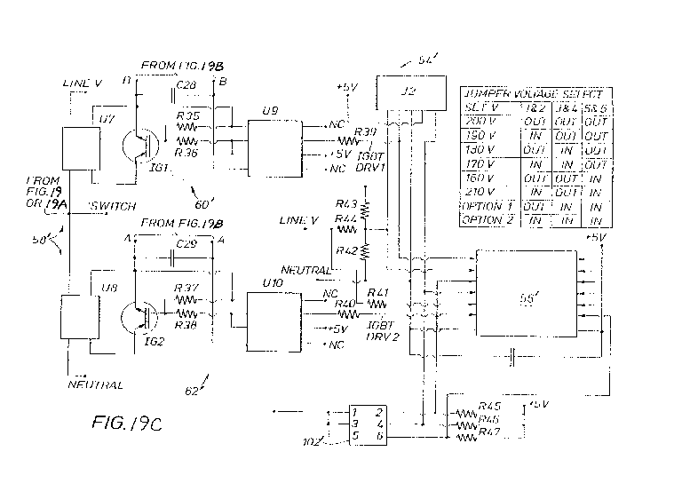
102211 FIGS. 19-19C taken together show a second embodiment of a voltage
booster
apparatus 54'. FIG. 19 shows exemplary 120 Volt transformer 66'. FIG. 2A shows
exemplary 230 Volt transformer 68'. The wiring arrangements are different in
FIGS. 19 and
19A. The windings for the 120 Volt transformer 66' (FIG. 19) are in parallel,
and the
windings for the 230 Volt transformer 68' (FIG. 19A) are in series. The same
transformer
66', 68' may be used for 120 Volt and for 230 Volt by configuring the wiring
arrangements as
shown: parallel for 120 Volts and series for 230 Volts. However, different
66', 68'
transformers may be used as well. The transformer may be a single voltage type
specifically
for 230 V, 120 V, or any other voltage range. Other transformers with
different current
ratings are also contemplated. Only one such transformer 66', 68' would be
connected with
the system at a time. FIG. 19B shows two isolated DC power supplies (50',
52'), power
supply 63', and power supply regulation circuitry 64'. FIG. 19C shows
microprocessor 56'
and IGBT switch device 58'. Switch 58' comprises first diode bridge circuit
U7, first IGBT
circuit 60', second diode bridge circuit U8, and second IGBT circuit 62'.
51
CA 02811711 2013-03-19
WO 2012/050635
PCT/US2011/032840
102221 Turning to FIG. 19, secondary windings 72A and 72B of 120 Volt
transformer 66'
are in parallel between the input line hot terminal 78' and the output line
hot terminal 80'.
Hot input line 74' to hot output line 76' passes through the transformer
secondary windings
72A and 72B at all times, and is not switched. The transfoimer 66' primary
windings 70A
and 70B have first end or first line 82' connected to hot input terminal 78'
through connector
F5, and second end or second line 84' connected through connector F14 with
electronic
switch 58'. Switch 58' allows transformer 66' second line 84' to either (1)
connect with first
line 82' of the transformer 66' primary windings 70A, 70B, thereby short-
circuiting the
transformer 66', or (2) connect with neutral line 90'. Connectors F4 through
F17 are Faston
type connectors. The connectors (F1 to F17) allow for the removably plugging
in or
connecting of different rated transfoimers (66', 68'), such as 120V and 230V.
Other types of
connectors are also contemplated.
102231 In FIG. 19A, the 230V transformer 68', like the 120V transformer
66', may be
removably plugged or unplugged into the same connectors (Fl to F17). However,
the wiring
arrangement for transformer 68' is different. Other arrangements of wiring and
connection
are also contemplated. The transformer 68' secondary windings 92A and 92B are
in series
between the input line hot terminal 78' and the output line hot terminal 80'.
Hot input line
52
CA 02811711 2013-03-19
WO 2012/050635
PCT/US2011/032840
85' passes through connector F8 to terminal 78'. Hot output line 87' passed
through
connector Fit to terminal 80'. Hot input line 85' to hot output line 87'
passes through the
transformer secondary windings 92A and 92B at all times, and is not switched.
The
transformer 68' primary windings 94A and 94B have first end or first line 96'
connected to
hot input terminal 78' through connector F5, and second end or second line 98'
connected
through connector F14 with electronic switch 58'. Switch 58' allows
transformer 68' second
line 98' to either (1) connect with first line 96' of the transformer 68'
primary windings 94A,
94B, thereby short-circuiting the transformer 68', or (2) connect with neutral
line 90'.
102241 As can now be understood, the same transformer may be used for 120 V
and 230
V, with the connections shown in FIGS. 19-19A configuring the transformer for
120 V (FIG.
19) or 230 V (FIG. 19A) as desired. When the transformer primary windings
second line 84',
98' is switched to neutral, the secondary voltage adds to the mains input
voltage, thereby
providing boosted output voltage at hot output terminal 80'. An electric load
may be
connected with output terminal 80'. The winding voltage is phased to be
additive to the
incoming AC line voltage, thereby providing boosted voltage when needed.
102251 When switch 58' is switched to the other state or condition,
removing the primary
windings second line 84', 98' connection from neutral and connecting it with
respective first
53
CA 02811711 2013-03-19
WO 2012/050635
PCT/US2011/032840
line 82', 96', the transformer primary windings (70A, 70B) or (94A, 94B) are
short circuited.
By creating a short circuit in the non-boosted position, the transformer is
disconnected and
does not consume any power. Also, since the primary is shorted out, and the
secondary is
permanently connected between hot input terminal 78' and hot output telininal
80', there will
be substantially no reactive component of the current on the secondary
windings side and
therefore substantially no inductively reactive losses during non-boost
operation. The only
impediments to the passage of the AC power from input 78' to output 80' will
be the very
small ohmic resistance of the copper or other windings of the secondary
windings. As with
the first embodiment, the switching is advantageously performed on the
transformer primary
side, which allows for switching with less current. Also, there is
substantially no interruption
of power during the switching period.
[0226] Turning
to FIG. 19B, three independent power supplies (50', 52', 63') may provide
power to switching network 58' and/or microprocessor 56'. First power supply
50' provides
power to first IGBT circuit 60', and second power supply 52' provides power to
second
IGBT circuit 62'. It is contemplated that the arrangement could be reversed.
Third power
supply 63' may provide power for microprocessor 56', LEDs, and Optos. Other
arrangements are also contemplated. First and second power supplies (50', 52')
may each
54
CA 02811711 2013-03-19
WO 2012/050635
PCT/US2011/032840
provide twelve (12) volt DC power, and third power supply 63' may provide five
(5) volt DC
power, although other power supplies and voltages are also contemplated,
including
alternating current. It is contemplated that there may be only one power
supply, or more than
three power supplies.
[0227] In FIG. 19C, first diode bridge circuit U7 is configured with first
IGBT circuit 60'
comprising first IGBT device IG1 and first optically isolated IGBT/MOSFET
driver U9.
Second diode bridge circuit U8 is configured with second IGBT circuit 62'
comprising
second IGBT device IG2 and second optically isolated IGBT/MOSFET driver U10.
Diode
bridge circuits U7, U8 are used to steer the current positive and negative
half cycles to arrive
at a condition known as unidirectional half cycles. This enables the use of a
single IGBT
device IG1 and IG2 since the IGBT is a unidirectional device. MOSFET devices
are also
contemplated.
[0228] Switch 58' functions like a single pole, double throw (SPDT) switch,
sometimes
referred to as a "changeover switch." When the respective IGBT device IG1 or
IG2 is in an
OFF condition, state, or position, then no AC current flows through the
respective diode
bridge U7, U8. When the respective IGBT device IG1 or IG2 is in an ON
condition, state, or
position, then AC current flows through the respective diode bridge U7, U8.
Microprocessor
CA 02811711 2013-03-19
WO 2012/050635
PCT/US2011/032840
56' measures the AC incoming line voltage, such as in line 100', and decides
the voltage level
at which the increased voltage should be employed. Three small jumper blocks
or 3 x 2
header 102' may allow the selection of the six (6) voltages as shown in Table
1 above and in
FIG. 19C. Other predetermined voltage settings are also contemplated. Other
numbers of
jumper blocks or header 102' are also contemplated. The microprocessor 56'
operates and
controls the IGBT switch device 58' to maintain the selected voltage.
102291 The microprocessor 56' may utilize detection of the zero voltage
crossing point of
the incoming AC mains voltage. This zero cross detection is used to assure
correct timing of
the switching of the IGBT devices IG1 and I62. Zero cross timing eliminates
the possibility
of both devices I61 and I62 being on at the same time. FIGS. 5 and 6 propose
an
oscillogram and circuitry diagram, respectively, of a volts zero crossing
point detennining
means that is contemplated. Other types of volts zero crossing point
determining means are
also contemplated. Hysteresis may be employed to eliminate any erratic
switching around
the threshold point set by the jumpers 102'.
102301 In FIGS. 19-19C, components R30 to R47 are resistors, components C20
to C29
are capacitors, components D10 and D1 1 are diodes, component Z1 is a
transorb,
components Z2 to Z4 may be (Schottky type) diodes, component Z5 is a Zener
diode,
56
CA 02811711 2013-03-19
WO 2012/050635
PCT/US2011/032840
components IC! and IG2 are IGBT transistors, component TRA1 is a transformer,
component U2 is a switching regulator, component U3 is an Opto isolator,
components U4 to
U6 are linear regulators, components U7 and U8 are diode bridge circuits or
bridge rectifiers,
component U9 and U10 are optically isolated IGBT/MOSFET drivers, and component
J2 is a
1 x 5 header.
102311 As can now be understood, all switching may be perfoinied at
substantially less
current on the primary side, such as primary side (10A, 10B) of the
transformer 41', than on
the secondary side, such as secondary side (2A, 2B) of transformer 41'. Since
the secondary
windings are permanently connected, and the boost switching is performed on
the primary
side, there will be substantially no interruption of electricity during the
switching period.
This cannot be achieved when switching is performed on the secondary side.
Different
embodiments of electronic switches (16', 58') are employed to short circuit
the transformer
primary when it is not in use, thereby eliminating the reactive component of
the current from
the secondary winding side. The transformer is only active during the voltage
boost period.
The amount of boost or increase may be selected by the transformer ratio.
Transformers with
different ratios and/or current ratings may be removably connected with the
system. The
apparatus may be used for universal operation for AC 120 Volts to 250 Volts.
The apparatus
57
CA 02811711 2013-03-19
WO 2012/050635
PCT/US2011/032840
size may be relatively small. There may be very small thermal dissipation. The
apparatus
may be cost effective and reliable. The apparatus may be used to supply
increased voltage
for electric loads, including residential, industrial or commercial.
102321 Although two switching network embodiments are shown in FIGS. 18A-19C,
other
embodiments are contemplated, including, but not limited to, the switching
performed with
(1) a diode bridge in conjunction with an IGBT, (2) a diode bridge in
conjunction with a
power MOSFET, (3) a diode bridge in conjunction with a mechanical switch,
relay, contactor
or any other type of mechanical switch, (4) a diode bridge in conjunction with
an
SCR/Thyristor or a TR1AC, (5) TRIAC, (6) SCR/Thyristor devices arranged in an
inverse
parallel arrangement, or (7) a mechanical switch, relay, contactor or any
other type of
mechanical switch. The switches may be used to provide a first state,
condition, or position
short circuiting the primary windings, and a second state, condition, or
position for adding the
transformer secondary voltage with the mains input voltage. In all
embodiments, other
transformer primary windings taps are contemplated to provide different boost
levels at a
variety of threshold voltages. The taps may allow a certain number of turns of
the
transformer primary winding to be selected, providing a transformer with a
variable turns
58
CA 02811711 2013-03-19
WO 2012/050635
PCT/US2011/032840
ratio. For all embodiments, there may be multiple taps on the primary windings
selected by
the microprocessor for providing differing boost levels at differing input
voltage levels.
[0233] Managing Electrical Power Usage
102341 The IGBT/FET-based device 1 shown in FIGS. 1-17 and the voltage
booster
system 30' shown in FIG. 18A-19C may work together to manage electrical power
usage.
During a first predetermined time period, such as when blackouts are not
anticipated, the DSP
controls the IGBT/FET-based device 1 shown in FIG. 1 to supply a predetermined
voltage
that is less than the AC incoming line voltage. Phase input connections 2 are
provided for
inputting analog signals into the device 1. The magnetic flux concentrator 3
(or a current
transformer) senses the incoming analog signal and the volts zero crossing
point detector 5
determines the zero volts crossing point of the signal. The positive half
cycle and negative
half cycle of the signal is identified and routed to the digital signal
processor 10 for
processing the signal. The signal is reduced by the driver control 15 via
pulse width
modulation and the reduced amount of energy is outputted, thereby yielding an
energy
savings for an end user. As shown in FIG. 1, real time clock module 49 is
connected with the
DSP 10. The real time clock module 49 may be used to set the predetermined
time periods.
59
CA 02811711 2013-03-19
WO 2012/050635
PCT/US2011/032840
[0235] The microprocessor 26' shown in FIG. 18C may measure the AC incoming
line
voltage, and compare it with the predetermined voltage. When the AC incoming
line voltage
is higher than the predetermined voltage, the microprocessor controls the
switching network
16' shown in FIG. 18A on the primary windings side of the transformer to short
circuit the
primary windings. When the measured voltage is less than the predetermined
voltage, and
voltage increase is needed, such as during a brownout condition, the
microprocessor 26'
controls the switching network 16' to connect one end of the primary windings
to neutral,
removing the short circuit from the transformer and allowing the secondary
voltage to add to
the mains input voltage to provide a boosted output voltage through the hot
output line of the
secondary windings side of the transfoliner. The voltage may be increased to
the
predetermined voltage. The secondary windings are not switched.
[0236] During a second predetermined period of time, such as when blackout
conditions
are anticipated, the DSP 10 controls the IGBT/FET-based device 1 shown in FIG.
1 to supply
an allocated amount of power, which may be predetermined. The DSP 10 and/or
the
microprocessor 26' monitors power consumption, which may be displayed. When
the power
consumption exceeds the allocated amount, the DSP 10 may shut off the power.
CA 02811711 2013-03-19
WO 2012/050635
PCT/US2011/032840
102371 Alternatively, when the consumed power exceeds the allocated power,
a signal
may be sent alerting the need to reduce power usage. In FIG. 20, signal module
100 is
connected with DSP 10 and may provide the signal. The signal may be audible,
visible, or
other means. The signal module may be a buzzer module, although other modules
are also
contemplated. Wirelessly controlled electrical outlets may be used to
selectively reduce the
load in response to the signal. If the load has not been adequately reduced
after a
predetermined amount of time, the DSP 10 may shut off power. The consumer may
then
reduce some load, and initiate a command to turn the power back on. The
command may be
initiated by changing the condition of a switch, including manually and/or
wirelessly. If the
load has still not been adequately reduced after the power has been restored,
then the DSP
may again shut off the power. Alternatively, the DSP may provide another
signal that may
again alert that the load must be reduced. If the consumed power is not
reduced sufficiently
after a predetermined amount of time, then the DSP may shut off power through
the hot
output line for the duration of the second predetermined time period.
[0238] Further alternatively, when the consumed power exceeds the allocated
power, the
DSP may shut off power to predetermined electrical outlets, while providing
power to other
electrical outlets, to reduce the overall power usage to the allocated power
amount. The
61
CA 02811711 2013-03-19
WO 2012/050635
PCT/US2011/032840
system may use wirelessly controlled electrical outlets that may be
automatically shut-down
to meet the predetermined power amount. The system and method may use preset
consumer
preferences to reduce the power consumed. The system may be monitored,
operated and
adjusted wirelessly.
102391 Energy allocation, such as described above, allows consumers to
enjoy electrical
power for key appliances rather than have no power at all. There are many
times that this
action is necessary where there is insufficient electrical power for all
consumers. Under such
conditions, the electrical company may desire to provide a reduced or
allocated service to all
consumers, rather than provide service to some consumers and no service at all
to others. The
consumer may become part of the solution rather than part of the problem.
102401 Through wireless communication there is the ability to communicate
between
controllers, adapters, and input devices. The display device may utilize an
off the shelf
computer, iPad, smart phone, or other input device using a keyboard, touch
screen or
combination thereof. Other devices are also contemplated. An iPad is available
from Apple
Inc. of Cupertino, California. While an input device may be used to wirelessly
monitor,
adjust settings, or adjust control parameters, the system may function
completely on its own,
independent of the input device. Furthermore, the main unit may have full
wireless
62
CA 02811711 2013-03-19
WO 2012/050635
PCT/US2011/032840
communications to enable remote control of the aforementioned power outlet and
adapters.
The system may provide full lighting and environment control. The system may
allow for a
consumer's power usage profile to be input and implemented for power
allocation and
selective power reduction. The system and method may provide dynamic power
allocation.
102411 As can now be understood, the system and method is a conservation power
management system that is installed at the point of consumption. The
implementation does
not require any immediate increase in power generation, nor does it require
any immediate
enhancement of the power grid. The solution uses an energy management system
that saves
energy, reduces brown outs and blackouts, and manages usage to reduce costs to
the
consumer and the electrical generating and distribution company. The
management system
results in a reduction in copper losses, thereby releasing energy previously
wasted as heat and
at a financial loss to the electrical company. The conserved energy can be
provided to
additional consumers, thereby providing additional income to the electrical
utility, at no
additional costs.
[0242] The system and method have at least eight main features: (1) energy
conservation
and user cost savings, (2) voltage stabilization, (3) uniform electricity
costs to consumers, (4)
63
CA 02811711 2013-03-19
WO 2012/050635
PCT/US2011/032840
copper loss reduction, (5) hydrocarbon emission mitigation, (6) brownout
mitigation, (7)
blackout mitigation, and (8) energy allocation.
102431 The system and method provide energy conservation and user cost
savings.
Electrical power is typically delivered to the consumer at a nominal voltage
of 120/127/230
Vrms. This is the target voltage that the electrical company aims to supply.
This voltage can
disadvantageously fluctuate by plus or minus 10%, or more, within the power
company
specification, often by a much greater margin. Appliance manufacturers, well
aware of the
power shortcomings, design their appliances for the low (minus 10%) end of the
supply
voltage and design the devices to withstand the high (plus 10%) end of the
supplied voltage.
At the low end, the appliance will perform its task as specified. However, at
any voltage
above the low voltage, the appliance will be over supplied and will waste
electrical energy at
a cost to the consumer. The system and method minimize this situation. The
invention
regulates the AC voltage at the selected low voltage, thereby saving energy.
102441 The system and method provide voltage stabilization. In extreme
cases where the
delivered voltage falls below the low voltage, the system and method solve
this problem by
boosting the incoming voltage, such as to allow the voltage regulation to
occur. Unlike
voltage boosters that are available for single appliances, the boost section
of the system
64
CA 02811711 2013-03-19
WO 2012/050635
PCT/US2011/032840
maintains the voltage at the low end for the whole home or business. Not only
does this
improve the quality of service for the consumer, it also allows the removal of
unsightly
boosters, used in some countries, from the vicinity of specific appliances so
equipped.
102451 The
system and method provide uniform electricity cost to consumers. In a typical
community, the consumers are charged inconsistently for the same amounts of
electrical
power required, which is a result of inconsistent voltages being supplied to
the community.
These losses result from copper losses. Electrical conductors impede the flow
of electrical
current. This shortcoming of all conductors can be planned for, and larger
copper conductors
can be employed. Increasing the size of the conductor reduces the copper
losses.
Unfortunately, the existing power distribution networks were not designed to
carry the power
needs of emerging economies where affluence is accompanied by the desire, on
the part of
the consumer, to have appliances and entertainment systems to complement the
improved life
style. The result is that for a community, the power delivered to the consumer
closest to the
main electricity transformer, has a much higher voltage than that which is
delivered to the
consumer furthermost removed from the transformer. This unfair situation
results in the
consumer closest to the transformer paying for more energy than the consumer
at the other
end, even if both consumers have identical appliances and a similar lifestyle.
The product of
CA 02811711 2013-03-19
WO 2012/050635
PCT/US2011/032840
electrical voltage and current is watts, and higher voltage results in higher
wattage. Wattage
per hour is what the consumer pays for. This unfair power situation may be
resolved by the
system and method.
102461 The system and method provide copper loss reduction. Copper losses are
the
cumulative power distribution losses experienced in all power distribution
networks. In most
emerging economies the power distribution network is not capable of sustaining
the loading
imposed when a community attempts to consume quantities of power that the
network was
not designed for. This situation usually results from an increase in
affluence, which is
generally accompanied by the ownership of consumer items like air
conditioners, central
heating, televisions, washers, audio and improved lighting. When the feeder
supplying power
to the homes in such a community experiences excessive loading, the electrical
resistance,
present in all conductors, becomes significant, and a portion of the supplied
voltage appears
across the resistance of the conductor. The product of this voltage together
with the current
from many consumers causes a power loss (Watts) within the conductor that is
dissipated as
heat. This represents a major loss of revenue to the electrical company. With
the system and
method installed and implemented in the homes associated with this section of
the network,
66
CA 02811711 2013-03-19
WO 2012/050635
PCT/US2011/032840
the power that was otherwise wasted may then be available to other consumers
and may
result in an improved revenue stream to the electrical company.
102471 The system and method provide hydrocarbon emission mitigation.
Hydrocarbon
emissions exist when fossil fuels (oil, gas or coal) are used to generate
electrical power. The
system and method manage the power being consumed with considerable
conservation, at the
point of consumption. The effect is twofold: first, a reduction in electrical
energy results in a
reduction in fossil fuel being consumed with the attendant savings of carbon
emissions; and
second, this can defer the immediate need for additional generation capacity.
Either way
benefits are accrued and directly affect the carbon bond situation in a
positive way.
102481 The system and method provide brownout mitigation. The system and
method,
just by their implementation, mitigates this problem. However, associated with
the system
and method is a feature where, at known times susceptible to brownout, the
device can be
programmed to, automatically, apply an additional percentage of voltage
reduction. Under
such circumstances, the loading on the network is further reduced and results
in further
copper loss reduction.
[0249] The system and method provide blackout mitigation. The times of
blackouts are
usually well known to the electrical company. The system and method, at known
times
67
CA 02811711 2013-03-19
WO 2012/050635
PCT/US2011/032840
susceptible to blackout, automatically monitor the power usage, alert the
consumer, and
allocate the power such that every consumer gets their rationed amount.
[0250] In one embodiment, when the set time is activated and the allocated
wattage is
being exceeded, an audible warning device alerts the consumer to shed load.
Sometime later,
if insufficient load has been shed, the system can be automatically shut down.
At this point
the consumer can shed some load and then change the condition of a switch to
bring the
system back on line. If insufficient load has been shed, the audible warning
device will again
alert the consumer to shed more load. If the consumer does not respond, the
system may be
set to shut down power for the remaining timed period. Other embodiments are
contemplated. Various scenarios can be invoked in accordance with the local
situation,
desires, and needs of the electricity company, at their discretion.
Furtheimore, wirelessly
controlled electrical outlets can be utilized so that the appropriate devices
can be
automatically shut-down to meet the required load shedding requirements in
relation to the
allocated power.
[0251] The system and method provide energy allocation. Energy allocation
described
above allows consumers to enjoy electrical power for key appliances rather
than have no
power at all. There are many times that this action is necessary where there
is insufficient
68
CA 02811711 2013-03-19
WO 2012/(15(1635
PCT/US2011/032840
electrical power to go around everyone. Under such a scenario, it is fair to
provide a reduced
service to everyone to an allocated amount rather than provide service to some
and no service
at all to others. Each consumer is part of the solution rather than part of
the problem.
102521 It is to be understood that while embodiments are illustrated, they
are not to be
limited to the specific form or arrangement of parts herein described and
shown. It will be
apparent to those skilled in the art that various changes may be made without
departing from
the scope of the invention and the invention is not be considered limited to
what is shown and
described in the specification and drawings.
69