Note : Les descriptions sont présentées dans la langue officielle dans laquelle elles ont été soumises.
CA 02816184 2013-04-26
WO 2012/055780 PCT/EP2011/068424
DESCRIPTION
OPTIMIZED SEMICONDUCTOR PACKAGING IN A THREE-DIMENSIONAL STACK
BACKGROUND
WU The present application relates generally to an
improved data processing apparatus and method and more
specifically to mechanisms for optimizing semiconductor
packing in a three-dimensional stack.
Nom Three-dimensional (3D) integration provides
performance improvements for microprocessor architectures
through the increased interconnectivity between tiers within
the chip stack. However, the electrical off-stack
connectivity (signals and power) is still implemented on only
one surface of the chip stack and does not scale with the
number of tiers. With further scaling of complementary metal-
oxide-semiconductor (CMOS) transistors the number of C4s will
not be sufficient even for single dies, due to the slow
reduction in C4 pitch over time. For 3D chip stacks, this
results in sever design constraints and reduces the
performance gain possible from vertical integration.
SUMMARY
[0003] In one illustrative embodiment, a three-dimensional
very-large-scale integration (VLSI) device is provided. The
three-dimensional VLSI device comprises a processor layer
coupled to at least one signaling and input/output (I/O) layer
via a first set of coupling devices. The three-dimensional
VLSI device further comprises a power delivery layer coupled
to the processor layer via a second set of coupling devices.
In the three-dimensional VLSI device, the power delivery layer
CA 02816184 2013-04-26
WO 2012/055780 PCT/EP2011/068424
- 2 -
is dedicated to only delivering power and does not provide
data communication signals to the elements of the three-
dimensional VLSI device. Also in the three-dimensional VLSI
device, the at least one signaling and input/output (I/O)
layer is dedicated to only transmitting the data communication
signals to and receiving the data communications signals from
the processor layer and does not provide power to the elements
of the processor layer.
KOM In another illustrative embodiment, a data processing
system is provided. The data processing system comprises a
processor layer coupled to at least one signaling and
input/output (I/O) layer via a first set of coupling devices.
The data processing system further comprises a power delivery
layer coupled to the processor layer via a second set of
coupling devices. In the data processing system, the power
delivery layer is dedicated to only delivering power and does
not provide data communication signals to the elements of the
data processing system. Also in the data processing system,
the at least one signaling and input/output (I/O) layer is
dedicated to only transmitting the data communication signals
to and receiving the data communications signals from the
processor layer and does not provide power to the elements of
the processor layer.
[0005] In yet another illustrative embodiment, a method, in a
data processing system, is provided for optimizing
semiconductor packing in a three-dimensional very-large-scale
integration (VLSI) device. The illustrative embodiment
couples a processor layer to at least one signaling and
input/output (I/O) layer using a first set of coupling
devices. The illustrative embodiment also couples a power
delivery layer to the processor layer using a second set of
coupling devices. In the illustrative embodiment, the power
delivery layer is dedicated to only delivering power and does
CA 02816184 2013-04-26
WO 2012/055780 PCT/EP2011/068424
- 3 -
not provide data communication signals to the elements of the
three-dimensional VLSI device. In the illustrative
embodiment, the at least one signaling and input/output (I/O)
layer is dedicated to only transmitting the data communication
signals to and receiving the data communications signals from
the processor layer and does not provide power to the elements
of the processor layer.
[0006] These and other features and advantages of the present
invention will be described in, or will become apparent to
those of ordinary skill in the art in view of, the following
detailed description of the example embodiments of the present
invention.
CA 02816184 2013-04-26
WO 2012/055780
PCT/EP2011/068424
- 4 -
BRIE F DESCRIPTION OF THE SEVERAL VIEWS OF THE DRAWINGS
[0007] The invention, as well as a preferred mode of use and
further objectives and advantages thereof, will best be
understood by reference to the following detailed description
of illustrative embodiments when read in conjunction with the
accompanying drawings, wherein:
[0008] Figure 1 depicts a block diagram of a data processing
system with which aspects of the illustrative embodiments may
advantageously be utilized;
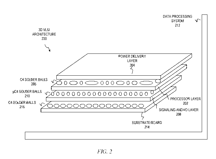
[0009] Figure 2 depicts one example of a three-dimensional
(3D) very-large-scale integration (VLSI) architecture in
accordance with an illustrative embodiment;
[001O] Figures 3A-3C depict one example of a power delivery
system implementation in accordance with an illustrative
embodiment;
KOM Figures 4A-4G depict another example of a power
delivery system implementation in accordance with an
illustrative embodiment; and
[0012] Figure 5 depicts a 3D VLSI architecture comprising a
high-speed signaling and I/O layer coupled to a
substrate/board via a second plurality of C4 solder balls in
accordance with an illustrative embodiment.
CA 02816184 2013-04-26
WO 2012/055780 PCT/EP2011/068424
- 5 -
DETAILED DESCRIPTION
[0013] One illustrative embodiment provides a mechanism for
optimizing semiconductor packing in a three-dimensional (3D)
stack by dedicating one side of the 3D to power delivery and
the other side of the 3D stack to high speed signaling
delivery. Power delivery and high speed signal issues for the
3D stack are then solved by use of through silicon vias
(TSVs). In another illustrative embodiment, delivery of
multiple power voltages required by a 3D stack are provided
via a heat sink that provides an integrated power delivery and
distribution to the various integrated circuits of the 3D
stack. In yet another illustrative embodiment, delivery of
multiple power voltages required by a 3D stack are provided
via a laminate structure between the top of a 3D chip stack
and a heat dissipation device, such as a heat sink, a cold
plate, or the like, that provides power delivery for multiple
power domains to the various integrated circuits of the 3D
stack and obstructs the heat conduction only minimally.
[0014] Thus, the illustrative embodiments may be utilized in
many different types of data processing environments including
a distributed data processing environment, a single data
processing device, or the like. In order to provide a context
for the description of the specific elements and functionality
of the illustrative embodiments, Figure 1 is provided
hereafter as example environments in which aspects of the
illustrative embodiments may be implemented. While the
description following Figure 1 will focus primarily on a
single data processing device implementation for a three-
dimensional processor core architecture that provides
performance improvement through an increased interconnectivity
and higher packaging density, this is only an example and is
not intended to state or imply any limitation with regard to
CA 02816184 2013-04-26
WO 2012/055780 PCT/EP2011/068424
- 6 -
the features of the present invention. To the contrary, the
illustrative embodiments are intended to include distributed
data processing environments and embodiments in which
performance improvement through an increased interconnectivity
and higher packaging density may be provided for a three-
dimensional processor core architecture.
[0015] Referring now to the drawings and in particular to
Figure 1, there is depicted a block diagram of a data
processing system with which aspects of the illustrative
embodiments may advantageously be utilized. As shown, data
processing system 100 includes processor units 111a-111n.
Each of processor units 111a-111n includes a processor and a
cache memory. For example, processor card 111a contains
processor 112a and cache memory 113a, and processor card 111n
contains processor 112n and cache memory 113n.
[0016] Processor units 111a-111n are connected to main bus
115. Main bus 115 supports a system planar 120 that contains
processor units 111a-111n and memory cards 123. The system
planar also contains data switch 121 and memory controller/
cache 122. Memory controller/cache 122 supports memory cards
123 that include local memory 116 having multiple dual in-line
memory modules (DIMMs).
[0017] Data switch 121 connects to bus bridge 117 and bus
bridge 118 located within a native I/O (NIO) planar 124. As
shown, bus bridge 118 connects to peripheral components
interconnect (PCI) bridges 125 and 126 via system bus 119. PCI
bridge 125 connects to a variety of I/O devices via PCI bus
128. As shown, hard disk 136 may be connected to PCI bus 128
via small computer system interface (SCSI) host adapter 130.
A graphics adapter 131 may be directly or indirectly connected
to PCI bus 128. PCI bridge 126 provides connections for
external data streams through network adapter 134 and adapter
card slots 135a-135n via PCI bus 127.
CA 02816184 2013-04-26
WO 2012/055780 PCT/EP2011/068424
- 7 -
[0018] An industry standard architecture (ISA) bus 129
connects to PCI bus 128 via ISA bridge 132. ISA bridge 132
provides interconnection capabilities through NIO controller
133 having serial connections Serial 1 and Serial 2. A floppy
drive connection, keyboard connection, and mouse connection
are provided by NIO controller 133 to allow data processing
system 100 to accept data input from a user via a
corresponding input device. In addition, non-volatile RAM
(NVRAM) 140, connected to ISA bus 129, provides a non-volatile
memory for preserving certain types of data from system
disruptions or system failures, such as power supply problems.
A system firmware 141 is also connected to ISA bus 129 for
implementing the initial Basic Input/Output System (BIOS)
functions. A service processor 144 connects to ISA bus 129 to
provide functionality for system diagnostics or system
servicing.
[0019] The operating system (OS) is stored on hard disk 136,
which may also provide storage for additional application
software for execution by data processing system. NVRAM 140
is used to store system variables and error information for
field replaceable unit (FRU) isolation. During system
startup, the bootstrap program loads the operating system and
initiates execution of the operating system. To load the
operating system, the bootstrap program first locates an
operating system kernel type from hard disk 136, loads the OS
into memory, and jumps to an initial address provided by the
operating system kernel. Typically, the operating system is
loaded into random-access memory (RAM) within the data
processing system. Once loaded and initialized, the operating
system controls the execution of programs and may provide
services such as resource allocation, scheduling, input/output
control, and data management.
CA 02816184 2013-04-26
WO 2012/055780 PCT/EP2011/068424
- 8 -
[0020] The illustrative embodiment may be embodied in a
variety of data processing systems utilizing a number of
different hardware configurations and software such as
bootstrap programs and operating systems. The data processing
system 100 may be, for example, a stand-alone system or part
of a network such as a local-area network (LAN) or a wide-area
network (WAN).
[0021] In known three-dimensional (3D) very-large-scale
integration (VLSI) architectures, power delivery is mixed with
high-speed signaling via C4 solder balls or pins to the 3D
VLSI chip stack. However, the possible number of C4 pins
which may be implemented limits that maximal input/output
(I/O) bandwidth and power delivery. To distribute the power
across the chip stack with minimal voltage drop, C4's on a
151pm pitch are needed. Hence, only very few C4's may be used
for signaling in the case of the limit of 44 C4's per square
millimeter, constraining the communication bandwidth.
Furthermore, by mixing the power delivery with the high-speed
signaling on one side of the 3D VLSI chip stack as is
currently done in known prior art, the thermal path is
minimized from the junction to the cooling device due to the
full access of the heat dissipation device on the opposed chip
stack surface whether the heat dissipation device is air or
liquid cooled. Similar mixing of power delivery with high-
speed signaling via C4 solder balls or pins is also
implemented in two-dimensional VLSI architectures. Thus,
while the below description is directed to 3D VLSI
architectures, the illustrative embodiments may also be
implemented for other dimensional VLSI architectures without
departing from the spirit and scope of the invention.
[0022] Figure 2 depicts one example of a three-dimensional
(3D) very-large-scale integration (VLSI) architecture in
accordance with an illustrative embodiment. In order to
CA 02816184 2013-04-26
WO 2012/055780 PCT/EP2011/068424
- 9 -
increase power delivery to support future complementary metal-
oxide semiconductor (CMOS) technologies, 3D VLSI architecture
200 comprises high-performance high-power processor layer 202
comprising a plurality of processor cores. Power delivery
layer 204 delivers power (Vdd) and ground from data processing
system 212 to high-performance high-power processor layer 202
via a first plurality of C4 solder balls 206 that are
optimized by size and/or geometry to deliver the required
power to each of the plurality of processor cores. While the
illustrative embodiments use C4 solder balls, other types of
coupling, such as copper pillars, may be used without
departing from the spirit and scope of the invention.
Possible implementations of power delivery layer 204 will be
discussed in detail below. Power delivery layer 204 may be
coupled to data processing system 212 using any type of
coupling mechanism, such as connectors formed on a system
board, cabling to a power supply, or the like. Using power
delivery layer 204 to provide power via one side of 3D VLSI
architecture 200 increases the number of C4 pins, as opposed
to known systems, and increases the power delivery above the
current limit of 100 watts per square centimeter.
Additionally, providing power via one side of 3D VLSI
architecture 200 decreases power noise that is currently
experienced on signal paths when mixed with power on the same
side of a 3D VLSI stack. Furthermore, TSVs needed to deliver
the power to processor layer 202 through substrate/board 214
and signaling and input/output (I/O) layer 208 may be removed
due to the direct power delivery from power delivery layer
204. Providing power from one side saves active silicon area
and does not cause macro redesigns due to protruding TSVs,
especially for large size memory blocks.
[0023] 3D VLSI architecture 200 also comprises high-speed
signaling and I/O layer 208 that comprises a plurality of
CA 02816184 2013-04-26
WO 2012/055780 PCT/EP2011/068424
- 10 -
high-speed signaling devices, which may include memory,
switches, memory storage controller, or the like. In order to
provide power to the high-speed signaling devices of high-
speed signaling and I/O layer 208, 3D VLSI architecture 200
provides micro C4 (pC4) layer 210. Power passes from power
delivery layer 204 through C4 solder balls 206, through
processor layer 202 via through silicon vias (TSVs) within the
silicon die of the processor layer, through pC4 layer 210, to
high-speed signaling and I/O layer 208. A contact pad on one
side of a die of processor layer 202 provides a connection of
one or more C4 solder ball in C4 solder balls 206 to a TSV in
processor layer 202, which passes power through processor
layer 202 to a contact pad on the other side of the processor
layer 202. The contact pad on the other side of processor
layer 202 provides a connection of each TSV to a pC4 solder
ball in pC4 layer 210. The use of micro pC4s in pC4 layer
210 allows higher interconnection density between processor
layer 202 and high-speed signaling and I/O layer 208. Power
may further pass from the pC4 layer 210 to one side of high-
speed signaling and I/O layer 208. A contact pad on the side
of high-speed signaling and I/O layer 208 provides a
connection of one or more pC4 in pC4 layer 210 to a TSV in
high-speed signaling and I/O layer 208, which passes power
through high-speed signaling and I/O layer 208 to a contact
pad on the other side of high-speed signaling and I/O layer
208. While only one high-speed signaling and I/O layer 208 is
depicted, the illustrative embodiments recognize that any
number of high-speed signaling and I/O layers may be
implemented and connected via additional layers of C4 solder
balls and TSVs.
[0024] Not only does pC4 layer 210 provide power to high-
speed signaling and I/O layer 208, but pC4 layer 210 also
provides connectivity for signaling between high-performance
CA 02816184 2013-04-26
WO 2012/055780 PCT/EP2011/068424
- 11 -
high-power processor layer 202 and high-speed signaling and
I/O layer 208 in a reverse fashion similar to the above
description for power delivery from one layer to another
layer. In order for high-speed signaling and I/O layer 208 to
transmit and receive signals with data processing system 212,
high-speed signaling and I/O layer 208 is coupled to
substrate/board 214 of data processing system 212 via a second
plurality of C4 solder balls 216. In addition to providing
connectivity for high-speed signaling and I/O, the second
plurality of C4 solder balls 216 may also provide connectivity
for ground as well as any low-power requirements that may not
be provided by power delivery layer 204 via pC4 layer 210.
Thus, high-speed signaling and I/O layer 208 comprises C4 pins
for signals mixed with ground pins for shielding, power
delivery, reference ground, and optional power for low(er)
power chips.
[0025] Therefore, 3D VLSI architecture 200 provides for
dedicated I/O for signal/ground via one side of the 3D stack
and voltage/ground via an opposite side of the 3D stack. For
connectivity to both high-performance high-power processor
layer 202 and high-speed signaling and I/O layer 208, the
illustrative embodiments provide different dedicated
technologies, such as C4s, pC4s, or macroC4s in different
geometries and pitches. Power delivery system 204 may provide
power via power pads or power strips, while inductive,
capacitive, or optical signal may be established via
substrate/board 214 to high-speed signaling and I/O layer 208.
The more flexible and granular arrangement of power pins for
different power domains of high-performance high-power
processor layer 202 decreases the restrictions associated with
mixing signaling and I/O with power. That is, the different
C4s pitch and geometries associated with a first plurality of
C4 solder balls 206 precisely mimic power domains of
CA 02816184 2013-04-26
WO 2012/055780 PCT/EP2011/068424
- 12 -
processing units/processing cores of high-performance high-
power processor layer 202. Furthermore, by not mixing power
with signaling and I/O the inductances in power delivery are
reduced and, thus, power noise in the signal and I/O paths is
reduced.
[0026] Figures 3A-3C depict one example of a power delivery
system implementation in accordance with an illustrative
embodiment. In the illustrative embodiment shown in Figure
3A, heat sink 302 comprises grooves 304 on one face of heat
sink 302 that will be coupled directly to a first plurality of
C4 solder balls providing connectivity to a high-performance
high-power processor layer. Each groove in grooves 304
comprises insulating material 310 between the metal of heat
sink 302 and conductors 312 which supply a path for power and
ground from a coupled power supply to the first plurality of
C4 solder balls. Insulating materials 310 may be comprised of
any insulating material such as ceramics, oxides such as
Aluminum Nitride (A1N), Aluminum Oxide (A1203), Silicon
Dioxide (SiO2), polymers, or the like. Heat sink 302 may be
comprised of any thermal conducting material such as copper,
aluminum, or the like. Conductors 312 may be comprised of any
electrical conducting material such as copper, aluminum, or
the like. Depending on the required voltages of the
processing units/processing cores of the high-performance
high-power processor layer, one or more of conductors 312 in
grooves 304 may supply one voltage, while another one or more
of conductors 312 supply a different voltage, such as 1.00
volt, 1.10 volts, 1.20 volts, or the like, while another one
or more of conductors 312 in grooves 304 may supply grounding
potential. Additionally, heat sink 302 may be used for ground
potential as long as heat sink 302 is coupled to the ground
potential of the data processing system. Use of exemplary
heat sink 302 provides very low impedance in power delivery,
CA 02816184 2013-04-26
WO 2012/055780 PCT/EP2011/068424
- 13 -
reduces noise, and reduces area impact associated with other
types of power delivery systems.
[0027] In Figure 3B, a face view of heat sink 302 is shown
indicating that grooves 304 extend across the face of heat
sink 302 that will be coupled directly to a first plurality of
C4 solder balls. This figure shows only the grooves without
the insulating material or the conducting material. In this
example, the architecture of the high-performance high-power
processor layer would be such that the various power pins of
the processing units/processing cores of the high-performance
high-power processor layer would need to be arranged such that
the C4 pins would align with grooves 304 of heat sink 302.
However, the illustrative embodiments are not limited to only
providing straight grooves 304.
[0028] Figure 3C depicts a face view of heat sink 302
indicating that grooves 304 are formed such that grooves 304
conform to the arrangement of the processing units/processing
cores of the high-performance high-power processor layer.
This figure shows only the grooves without the insulating
material or the conducting material. Thus, as opposed to
having grooves 304 extend across the face of heat sink 302 in
a straight line or all the way across the face of heat sink
302, grooves 304 may be formed such that the grooves 304
conform to the C4 pins arrangement associated with the
processing units/processing cores of the high-performance
high-power processor layer.
[0029] Thus, the heat sink of the illustrative embodiments
provides a conductive material for the heat sink to provide a
plurality of voltages to the high-performance high-power
processor layer without decoupling.
[0030] Figures 4A-4G depict another example of a power
delivery system implementation in accordance with an
illustrative embodiment. In the illustrative embodiment shown
CA 02816184 2013-04-26
WO 2012/055780 PCT/EP2011/068424
- 14 -
in Figure 4A, laminated power plane 400 is formed by
laminating a plurality of conductors 402 between a plurality
of insulating material 404. Depending on the required
voltages of the processing units/processing cores of the high-
performance high-power processor layer, one or more of
conductors 402 may supply one voltage, while another one or
more of conductors 402 supply a different voltage, such as
1.00 volt, 1.10 volts, 1.20 volts, or the like, while another
one or more of conductors 402 may supply grounding potential.
In order that the supplied voltage may be transferred to a
first plurality of C4 solder balls and then to the high-
performance high-power processor layer, each plane of
conductor 402 is solid at points 422 where through laminate
vias (TLVs) will be coupled to the conductor plane while areas
424 where the plane will be penetrated but not coupled to have
openings that will provide an insulating gap between a TLV and
the conductor.
[0031] Figure 4B depicts one illustration of the formation of
a laminated power plane in accordance with an illustrative
embodiment. As discussed above, laminated power plane 400 is
formed by laminating a plurality of conductors 402 between a
plurality of insulating material 404. In Figure 4B, a first
insulating layer 404a which is solid in composition is the
basis for laminated power plane 400, on top of the first
insulating layer 404a, is a first conducting layer 402a, which
is solid in areas where connecting TLVs will be formed and
open in areas where through TLVs will be formed. On top of
first conducting layer 402a is a second insulating layer 404b
which is solid in form. On top of the second insulating layer
404b, is second conducting layer 402b, which is solid in areas
where connecting TLVs will be formed and open in areas where
through TLVs will be formed. The process of forming laminated
power plane 400 continues until a final conducting layer 402n
CA 02816184 2013-04-26
WO 2012/055780 PCT/EP2011/068424
- 15 -
is layered on top of a final conducting layer 404n. After
laminated power plane is formed, the various TLVs are formed
such that each TLV couples to a specified one of the plurality
of conductors 402 while being insulated from other ones of the
plurality of conductors 402.
[0032] Figures 4C-4G depicts alternative methods for the
formation of a laminated power plane in accordance with an
illustrative embodiment. As discussed above, laminated power
plane 400 is formed by laminating a plurality of conductors
402 between a plurality of insulating material 404. In Figure
4C, in formation of laminated power plane 400, an additional
non-electrically conductive organic laminate layer 410 may be
inserted to provide mechanical stability to laminated power
plane 400 and to reduce the effective thermal expansion
coefficient of the thermal power laminate. In Figure 4D, the
plurality of insulating material 404 may be polyimide material
412, which are organic materials with an attractive
combination of characteristics, such as low relative
permitivity (low k), good thermal stability, chemical
inertness, and good adhesion to semiconductors and metals. In
Figure 4E, the plurality of insulating material 404 may be a
low temperature co-fired ceramic (LTCC) material 414 that
reduces thermal resistance compared to organic materials. In
Figure 4F, laminated power plane 400 may have an additional
thermal conductive silicon layer 416 formed on top of
laminated power plane 400 to increase thermal conductivity and
remove heat from the 3D stack. In Figure 4G, laminated power
plane 400 may have an additional thermal conductive silicon
layer 418 formed below laminated power plane 400 to increase
thermal conductivity and remove heat from the 3D stack;
however, this example requires additional length be added to
the TLVs.
CA 02816184 2013-04-26
WO 2012/055780 PCT/EP2011/068424
- 16 -
[0033] In addition to providing power to a first plurality of
C4 solder balls and then to high-performance high-power
processor layer, a laminated power plane, such as that shown
in Figures 4A-4G may also be configured to optimize thermal
dissipation away from high-performance high-power processor
layer. In Figure 5, 3D VLSI architecture 500 comprises high-
speed signaling and I/O layer 502 coupled to substrate/board
504 via a second plurality of C4 solder balls 506 in
accordance with an illustrative embodiment. High-performance
high-power processor layer 508 is coupled to high-speed
signaling and I/O layer 502 via through silicon via
(TSV)/micro C4 (pC4) layer 510. Further, power is delivered
to high-performance high-power processor layer 508 from power
delivery system 512 via a first plurality of C4 solder balls
514 and heat is removed from the 3D stack by heast dissipation
device 516, which may be either a cold plate or a heat sink,
coupled to power delivery system 512.
[0034] Power delivery system 512 may be formed in any one of
the methods discussed in Figure 4A-4G. In the depicted
example, power delivery system 512 is a laminate structure
comprising a plurality of conductors 518 between a plurality
of insulating material 520, one or more ground planes 522, and
an additional non-electrically conductive organic laminate
layer 524, with TLVs 526 connecting the first plurality of C4
solder balls 514 to one of the plurality of conductors 518 or
one or more ground planes 522. Additionally, in order to
optimize thermal dissipation away from high-performance high-
power processor layer 508, 3D VLSI architecture 500 may also
include thermal conduction vias 528 for thermal transfer of
heat though sidewalls from TLVs 526 that are directly coupled
to the high-performance high-power processor layer 508 to the
thermal conduction vias 528 that are coupled to ground planes
522 which is coupled to heat dissipation device 516. The
CA 02816184 2013-04-26
WO 2012/055780 PCT/EP2011/068424
- 17 -
thermal transfer of heat to ground planes 522 at sidewalls
reduces heat flux by surface enlargement at low thermal
conductivity interfaces for minimal temperature gradient.
The arrows within power delivery system 512 indicate heat
flow. 3D VLSI architecture 500 may also include ground
thermal conduction trees 530 for thermal transfer of heat
mainly through ground vias, which also take space above other
via locations. 3D VLSI architecture 500 may also include in-
plane heat collection 532 that reduces heat flux by surface
enlargement at low thermal conductivity interfaces.
[0035] Thus, an anisotropic thermal conductive power plane is
provided with high thermal conductivity normal to chip
backside. The conductive power plane may be sandwiched
between chip/stack and a cold plate in order to enable double
side electrical access. The thermal coupling of the thermal
power laminate to heat dissipation device 516 may be performed
in general with thermal interface materials (typically
particle filled polymers), such as thermal grease, thermal
adhesive, thermal pads, or by soldering or fusion bonding.
[0036] The description of the present invention has been
presented for purposes of illustration and description, and is
not intended to be exhaustive or limited to the invention in
the form disclosed. Many modifications and variations will be
apparent to those of ordinary skill in the art. The
embodiment was chosen and described in order to best explain
the principles of the invention, the practical application,
and to enable others of ordinary skill in the art to
understand the invention for various embodiments with various
modifications as are suited to the particular use
contemplated.