Note : Les descriptions sont présentées dans la langue officielle dans laquelle elles ont été soumises.
CA 02816522 2013-05-23
Digital Spread Spectrum Technique for
Electromagnetic Emission Reduction
TECHNICAL FIELD
[0001] The present disclosure relates generally to wager-based gaming
machines, and more
specifically to methods and devices for reducing electromagnetic (EM) emission
in a wager-
based gaming machine.
BACKGROUND
[0002] Typically, utilizing a master gaming controller, a gaming machine
controls various
combinations of devices that allow a player to play a wager game on the gaming
machine and
also encourage game play on the gaming machine. For example, a wager game
played on a
gaming machine usually requires a player to input money or indicia of credit
into the gaming
machine, indicate a wager amount, and initiate a game play. These steps
require the gaming
machine to control payment devices, including bill validators and coin
acceptors, to accept
money into the gaming machine and recognize user inputs from user interfaces,
including key
pads, button pads or touch screens, to determine the wager amount and initiate
game play.
After game play has been initiated, the gaming machine determines a wager game
outcome,
presents the game outcome to the player and may dispense an award of some type
depending
on the outcome of the wager game.
[0003] Modem gaming machines make liberal use of lights to enhance the visual
experience
of the player as well as to convey information regarding game events to the
player. Groups of
lights in a common location within the game machine are often connected to a
common
circuit board, or lighting board, which controls the operation of the lights.
The lighting board
selectively operates each light based on instructions received from the master
gaming
controller over a communications, or light bus. The light bus connecting the
master gaming
controller to the lighting board carries a clock signal to synchronize data
sent along the bus.
The light bus may be several feet long and a major source of EM emissions from
the game
machine.
1
[0004] The EM emissions from the light bus have a pronounced energy peak at a
fundamental frequency equal to the frequency of the clock signal, and also at
harmonics of the
fundamental frequency. Radiation at these frequencies can interfere with other
carrier signals
and devices. Such interference is known as electromagnetic interference (EMI).
[0005] The Federal Communication Commission (FCC) rules limit EM emission
levels for
gaming machines over a range of frequencies. In gaming machines, when emission
is
excessive at one or more frequencies, remedies that may be effective in
lowering emissions
include adding shielding components, adding ferrite clamps to harnesses (both
inter-assembly
signal harnesses and power/ground harnesses), improving grounding connections
between
system components, and board redesigning to add key signal filtering, improve
on-board
power/ground handing, or incorporate various signal integrity improvement
techniques at the
board level. These solutions often increase system cost because of added
material,
manufacturing, and labor costs. Furthermore, sometimes these remedies are not
reliably
replaced after system field maintenance because leaving them out has no
detrimental effect on
the functional operation of the gaming machine.
[0006] For the foregoing and other reasons, it would be desirable to provide
novel methods
and devices for reducing EM emission levels at low cost in gaming machines
that are not
subject to inadvertent removal or disablement.
SUMMARY
[0007] Various embodiments described or referenced herein are directed to
gaming
machines and methods implementing and using techniques for reducing EM
emissions in
gaming machines.
[0008] In some implementations, there is described a machine comprising: a
master clock
generator configured to generate a master clock signal; one or more
microprocessors
configured to: (1) divide the master clock signal to generate a bus clock
signal, the bus clock
signal having a fundamental frequency and fundamental spectral components at
harmonics of
the fundamental frequency, the fundamental spectral components each having a
fundamental
amplitude; and (2) generate a data signal; a signal processor configured to:
generate a spread
2
CA 2816522 2019-01-03
spectrum clock signal utilizing the bus clock signal and the master clock
signal by causing the
bus signal to jitter between two or more frequencies around the fundamental
frequency such
that the spread spectrum clock signal has a nominal frequency substantially
equivalent to the
fundamental frequency of the bus clock signal, wherein the data signal is
synchronized with
the spread spectrum clock signal, and wherein the spread spectrum clock signal
has nominal
spectral components at harmonics of the nominal frequency, the nominal
spectral components
each having a nominal amplitude less than the fundamental amplitude of a
fundamental
spectral component at the same harmonic; one or more elements controlled by a
synchronized
data signal and spread spectrum clock signal; and a bus communicatively
connecting the one
or more microprocessors and the signal processor with the one or more
elements, the bus
configured to carry the synchronized data signal and the spread spectrum clock
signal to the
one or more elements.
[0009]
[00010]
[00011]
[00012] In some implementations, the amount of jitter between the two or more
frequencies
around the fundamental frequency is based on the frequency of the master clock
signal.
[00013] In some implementations, the one or more microprocessors are further
configured to
provide wager game play on the gaming machine.
[00014] In some implementations, the one or more microprocessors are further
configured to
generate a data signal for controlling the one or more elements. The one or
more elements are
further configured to receive the data signal. The bus is further configured
to carry the data
signal to the one or more elements. In some implementations, the signal
processor is further
configured to synchronize the data signal with the spread spectrum clock
signal.
[00015] In some implementations, the signal processor is implemented with a
programmable
logic device such as a field programmable gate array (FPGA) or complex
programmable logic
device (CPLD). The programmable logic device is further configured to perform
address
3
CA 2816522 2019-01-03
decoding, signal direction control, or various logic functions in the gaming
machine unrelated
to lowering EM emissions.
[00016] In some implementations, the one or more elements include a lighting
board. The
gaming machine further includes a lighting display. The lighting board may
include light
emitting elements configured to provide lighting to the lighting display.
[00017] In some implementations, there is described a method for lowering EM
emissions in
a machine, the method comprising: generating, by a master clock generator, a
master clock
signal; generating, by one or more microprocessors: (1) a bus clock signal
having a
fundamental frequency and fundamental spectral components at harmonics of the
fundamental frequency, the fundamental spectral components each having a
fundamental
amplitude, wherein generating the bus clock signal comprises dividing, by the
one or more
microprocessors, the master clock signal; and (2) a data signal; generating,
by a signal
processor, a spread spectrum clock signal utilizing the bus clock signal and
the master clock
signal by causing the bus signal to jitter between two or more frequencies
around the
fundamental frequency such that the spread spectrum clock signal has a nominal
frequency
substantially equivalent to the fundamental frequency of the bus clock signal,
wherein the
data signal is synchronized with the spread spectrum clock signal, and wherein
the spread
spectrum clock signal has nominal spectral components at harmonics of the
nominal
frequency, the nominal spectral components each having a nominal amplitude
less than the
fundamental amplitude of a fundamental spectral component at the same
harmonic; and
sending a synchronized data signal and spread spectrum clock signal to one or
more elements
controlled by the synchronized data signal and spread spectrum clock signal
via a bus.
[00018]
[00019]
[00020] In some implementations, generating the spread spectrum clock signal
includes
causing the bus signal to jitter between two or more frequencies around the
fundamental
frequency while maintaining the nominal frequency.
[00021] In some implementations, the amount of jitter between the two or more
frequencies
is based on the frequency of the master clock signal.
4
CA 2816522 2019-01-03
[00022] In some implementations, the method includes providing wager game play
on the
gaming machine.
[00023] In some implementations, the method further includes generating a data
signal for
controlling the one or more elements. The one or more elements are further
configured to
receive the data signal. The method further includes sending the data signal
to the one or
more elements via the bus. In some implementations, the method further
includes
synchronizing the data signal with the spread spectrum clock signal with a
programmable
logic device and sending a synchronized data signal to the one or more
elements via the bus.
[00024] In some implementations, a programmable logic device such as an FPGA
or CPLD
generates the spread spectrum clock signal and performs address decoding,
signal direction
control, or other logic functions in the gaming machine unrelated to lowering
EM emissions.
[00024a] There is also described a signal-processing device comprising a
signal processor
configured to: receive a bus clock signal comprising a fundamental frequency
and
fundamental spectral components at harmonics of the fundamental frequency, the
bus clock
signal based on a master clock signal, the bus clock signal comprising a
divided master clock
signal, wherein the fundamental spectral components each comprise a
fundamental amplitude;
generate a spread-spectrum clock signal utilizing the bus clock signal and the
master clock
signal by causing the bus clock signal to jitter between two or more
frequencies around the
fundamental frequency such that the spread-spectrum clock signal has a nominal
frequency
substantially equivalent to the fundamental frequency of the bus clock signal;
receive a data
signal and synchronize the data signal with the spread-spectrum clock signal;
and transmit a
synchronized data signal and spread-spectrum clock signal to a controllable
element
controlled by the synchronized data signal and spread-spectrum clock signal
via a bus,
wherein the spread-spectrum clock signal comprises nominal spectral components
at
harmonics of the nominal frequency, wherein the nominal spectral components
each comprise
a nominal amplitude less than the fundamental amplitude of the fundamental
spectral
component at the same harmonic.
CA 2816522 2019-01-03
[00024b] There is also described a method of operating a signal processing
device, the
method comprising: receiving, by a signal processor, a bus clock signal
comprising a
fundamental frequency and fundamental spectral components at harmonics of the
fundamental frequency, the bus clock signal based on a master clock signal,
wherein the bus
clock signal comprises a divided master clock signal, and wherein the
fundamental spectral
components each comprise a fundamental amplitude; generating, by the signal
processor, a
spread-spectrum clock signal utilizing the bus clock signal and the master
clock signal by
causing the bus clock signal to jitter between two or more frequencies around
the fundamental
frequency such that the spread-spectrum clock signal has a nominal frequency
substantially
equivalent to the fundamental frequency of the bus clock signal; receiving, by
the signal
processor, a data signal and synchronizing the data signal with the spread-
spectrum clock
signal; and transmitting, by the signal processor, a synchronized data signal
and spread-
spectrum clock signal to a controllable element controlled by the synchronized
data signal and
spread-spectrum clock signal via a bus, wherein the spread-spectrum clock
signal comprises
nominal spectral components at harmonics of the nominal frequency, wherein the
nominal
spectral components each comprise a nominal amplitude less than the
fundamental amplitude
of the fundamental spectral component at the same harmonic.
[00024c] There is also described a signal-processing device comprising a
signal processor
configured to: receive a bus clock signal comprising a fundamental frequency
and
fundamental spectral components at harmonics of the fundamental frequency, the
bus clock
signal based on a master clock signal, wherein the fundamental spectral
components each
comprise a fundamental amplitude; generate a spread-spectrum clock signal
utilizing the bus
clock signal and the master clock signal by causing the bus clock signal to
jitter between two
or more frequencies around the fundamental frequency such that the spread-
spectrum clock
signal has a nominal frequency substantially equivalent to the fundamental
frequency of the
bus clock signal; receive a data signal and synchronize the data signal with
the spread-
spectrum clock signal; and transmit a synchronized data signal and spread-
spectrum clock
signal to a controllable element controlled by the synchronized data signal
and spread-
spectrum clock signal via a bus, wherein the spread-spectrum clock signal
comprises nominal
spectral components at harmonics of the nominal frequency, wherein the nominal
spectral
5a
CA 2816522 2019-01-03
components each comprise a nominal amplitude less than the fundamental
amplitude of the
fundamental spectral component at the same harmonic.
[00024d] There is also described a method of operating a signal processing
device, the
method comprising: receiving, by a signal processor, a bus clock signal
comprising a
fundamental frequency and fundamental spectral components at harmonics of the
fundamental frequency, the bus clock signal based on a master clock signal,
wherein the
fundamental spectral components each comprise a fundamental amplitude;
generating, by the
signal processor, a spread-spectrum clock signal utilizing the bus clock
signal and the master
clock signal by causing the bus clock signal to jitter between two or more
frequencies around
the fundamental frequency such that the spread-spectrum clock signal has a
nominal
frequency substantially equivalent to the fundamental frequency of the bus
clock signal;
receiving, by the signal processor, a data signal and synchronizing, by the
signal processor,
the data signal with the spread-spectrum clock signal; and transmitting, by
the signal
processor, a synchronized data signal and spread-spectrum clock signal to a
controllable
element controlled by the synchronized data signal and spread spectrum clock
signal via a
bus, wherein the spread-spectrum clock signal comprises nominal spectral
components at
harmonics of the nominal frequency, wherein the nominal spectral components
each comprise
a nominal amplitude less than the fundamental amplitude of the fundamental
spectral
component at the same harmonic.
[00024e] There is also described a signal-processing device comprising a
signal processor
configured to: receive a bus clock signal comprising a fundamental frequency
and
fundamental spectral components at harmonics of the fundamental frequency, the
bus clock
signal based on a master clock signal, the bus clock signal comprising a
divided master clock
signal, wherein the fundamental spectral components each comprise a
fundamental amplitude;
generate a spread-spectrum clock signal utilizing the bus clock signal and the
master clock
signal and causing the bus clock signal to jitter between two or more
frequencies around the
fundamental frequency such that the spread-spectrum clock signal has a nominal
frequency
substantially equivalent to the fundamental frequency of the bus clock signal;
receive a data
signal and synchronize the data signal with the spread-spectrum clock signal;
and transmit a
synchronized data signal and spread-spectrum clock signal to a lighting board
controlled by
5b
CA 2816522 2019-01-03
the synchronized data signal and spread-spectrum clock signal via a bus,
wherein the spread-
spectrum clock signal comprises nominal spectral components at harmonics of
the nominal
frequency, wherein the nominal spectral components each comprise a nominal
amplitude less
than the fundamental amplitude of the fundamental spectral component at the
same harmonic.
[00024f] There is also described a method of operating a signal processing
device, the
method comprising: receiving, by a signal processor, a bus clock signal
comprising a
fundamental frequency and fundamental spectral components at harmonics of the
fundamental frequency, the bus clock signal based on a master clock signal,
wherein the bus
clock signal comprises a divided master clock signal, and wherein the
fundamental spectral
components each comprise a fundamental amplitude; generating, by the signal
processor, a
spread-spectrum clock signal utilizing the bus clock signal and the master
clock signal by
causing the bus clock signal to jitter between two or more frequencies around
the fundamental
frequency such that the spread-spectrum clock signal has a nominal frequency
substantially
equivalent to the fundamental frequency of the bus clock signal; receiving, by
the signal
processor, a data signal and synchronizing, by the signal processor, the data
signal with the
spread-spectrum clock signal; and transmitting, by the signal processor, the
synchronized data
signal and the spread-spectrum clock signal to a lighting board via a bus,
wherein the spread-
spectrum clock signal comprises nominal spectral components at harmonics of
the nominal
frequency, wherein the nominal spectral components each comprise a nominal
amplitude less
than the fundamental amplitude of the fundamental spectral component at the
same harmonic.
[00024g] There is also described a signal-processing device comprising a
signal processor
configured to: receive a bus clock signal comprising a fundamental frequency
and
fundamental spectral components at harmonics of the fundamental frequency, the
bus clock
signal based on a master clock signal, wherein the fundamental spectral
components each
comprise a fundamental amplitude; generate a spread-spectrum clock signal
utilizing the bus
clock signal and the master clock signal by causing the bus clock signal to
jitter between two
or more frequencies around the fundamental frequency such that the spread-
spectrum clock
signal has a nominal frequency substantially equivalent to the fundamental
frequency of the
bus clock signal; receive a data signal and synchronize the data signal with
the spread-
spectrum clock signal; and transmit a synchronized data signal and spread-
spectrum clock
5c
CA 2816522 2019-01-03
signal to a lighting board controlled by the synchronized data signal and
spread-spectrum
clock signal via a bus, wherein the spread-spectrum clock signal comprises
nominal spectral
components at harmonics of the nominal frequency, wherein the nominal spectral
components
each comprise a nominal amplitude less than the fundamental amplitude of the
fundamental
spectral component at the same harmonic.
[00025] In some implementations, one or more of the elements include a
lighting board. In
some implementations, the lighting board includes light emitting elements, the
light emitting
elements configured to provide lighting to a lighting display.
[00026] Aspects of the invention may be implemented by networked gaming
machines, game
servers and other such devices. These and other features and benefits of
aspects of the
invention will be described in more detail below with reference to the
associated drawings. In
addition, other methods, features and advantages of the invention will be or
will become
apparent to one with skill in the art upon examination of the following
figures and detailed
description. It is intended that all such additional methods, features and
advantages be
included within this description, be within the scope of the invention, and be
protected by the
accompanying claims.
5d
CA 2816522 2019-01-03
CA 02816522 2013-05-23
BRIEF DESCRIPTION OF THE DRAWINGS
[00027] The included drawings are for illustrative purposes and serve only
to provide
examples of possible structures and process steps for the disclosed subject
matter. These
drawings in no way limit any changes in form and detail that may be made to
embodiments by
one skilled in the art without departing from the spirit and scope of the
disclosure.
[00028] Figure 1 shows an example of an exterior of a gaming machine 2,
configured
in accordance with some implementations.
[00029] Figure 2 shows an example of a gaming machine system 200,
configured in
accordance with some implementations.
[00030] Figure 3 shows an example of a control system 300 for lighting
boards of a
gaming machine, configured in accordance with some implementations.
[00031] Figure 4 shows a flowchart of an example of a method 400 for
reducing EM
emissions using a digital spread spectrum technique, performed in accordance
with some
implementations.
[00032] Figure 5 shows an example digital spread spectrum technique, in
accordance
with some implementations.
[00033] Figure 6 shows another example digital spread spectrum technique,
in
accordance with some implementations.
[00034] Figure 7 shows an example circuit 700 for performing the example
digital
spread spectrum technique shown in Figure 5, configured in accordance with
some
implementations.
6
CA 02816522 2013-05-23
DETAILED DESCRIPTION
[00035] Applications of gaming machines and methods according to one or
more
implementations are described in this section. These examples are being
provided solely to
add context and aid in the understanding of the present disclosure. It will
thus be apparent to
one skilled in the art that the techniques described herein may be practiced
without some or
all of these specific details. In other instances, well known process steps
have not been
described in detail in order to avoid unnecessarily obscuring the present
disclosure. Other
applications are possible, such that the following examples should not be
taken as definitive
or limiting either in scope or setting.
[00036] In the following detailed description, references are made to the
accompanying
drawings, which form a part of the description and in which are shown, by way
of illustration,
specific implementations. Although these implementations are described in
sufficient detail
to enable one skilled in the art to practice the disclosure, it is understood
that these examples
are not limiting, such that other implementations may be used and changes may
be made
without departing from the spirit and scope of the invention as defined by the
appended
claims.
[00037] The present subject matter provides gaming machines and methods
implementing and using techniques for reducing EM emissions in gaming
machines.
Although the current description primarily describes gaming machines, some
implementations
of the invention apply equally to other types of digital devices.
[00038] With reference to Figures 1 and 2, a gaming machine 2 may include
an
external cabinet 4 that houses one or more microprocessors 132 that
communicate with a
memory device 134. The one or more microprocessors and the memory device may
comprise
a master gaming controller that controls the operation of components in the
gaming machine
2 to present one or more games, receive player inputs from various input
devices, and control
other gaming machine functionalities.
[00039] The one or more microprocessors 132 may include general purpose or
specialized processors. The one or more microprocessors may be a logic system
including a
7
CA 02816522 2013-05-23
plurality of specialized logic devices configured to control various devices
and functionalities.
For instance, a first logic device may control input devices while a second
logic device may
control the generation of graphics for display.
[00040] The memory device 134 may include one or more memory modules, flash
memory or another type of memory that stores executable programs that are used
by the one
or more microprocessors. The memory device 134 can include any suitable
software and/or
hardware structure for storing data, including a tape, CD-ROM, floppy disk,
hard disk or any
other optical or magnetic storage media. The memory device 134 may also
include a) random
access memory (RAM) 140 for storing event data or other data generated or used
during a
particular game and b) read only memory (ROM) 142 for storing program code
that controls
functions on the gaming machine such as playing a game.
[00041] Although the one or more microprocessors 132 and the memory device
134
may reside in the gaming machine as shown in Figures 1 and 2, some
configurations provide
some or all of their functions at a central location or remote location. For
example, some of
the described functionality may be provided by a network server over a local
area network
(LAN), wide area network (WAN), Internet connection, microwave link, and the
like.
[00042] The gaming machine 2 further may further include various devices
that may be
under the control of the one or more microprocessors 132. In some
implementations, the
gaming machine may include one or more input devices 138. Such devices allow a
player to
interact with the gaming machine. Examples of input devices may include a pull
arm or input
switches 32 (e.g., a play button, a bet button or a cash out button). One or
more of these input
device functions could also be implemented on a touch screen, such as a touch
screen 33
which may be coupled with a display device screen to receive inputs from the
player.
[00043] In some implementations, the input devices may include a game
activation
device that may be used by the player to start any primary game or sequence of
events in the
gaming machine. The game activation device can be any suitable play activator
such as a "bet
one" button, a "max bet" button, or a "repeat the bet" button located on the
input switches 32
or the touch screen. The gaming machine may automatically activate game play
after
detecting user input via the game activation device. Other input devices may
include a key
8
CA 02816522 2013-05-23
pad for entering player tracking information, a card reader for entering a
magnetic striped card
containing player tracking information, a cash-out button for receiving a cash
payment or
other suitable form of payment corresponding to the number of remaining
credits.
[00044] In some implementations, the gaining machine may include payment
devices
116. The payment devices include devices for receiving and rewarding payment
in various
forms. Examples of payment devices include a coin acceptor 28, a bill
validator 30, and a
coin dispensing tray 38. In some examples, a ticketing system may be used to
accept and
print tickets for a cashless ticketing system.
[00045] In some implementations, the gaming machine may include
communication
ports for enabling communication of the gaming machine processor with external
peripherals,
such as external video sources, expansion buses, game or other displays, a
SATA port, a key
pad, or a network interface for communicating via a network.
[00046] In some implementations, the gaming machine may include a sound
generating
device coupled to one or more sound cards 136. The sound generating device may
include
one or more speakers 10 and 12 or other sound generating hardware and/or
software. The
speakers may be mounted and situated in the cabinet with an angled orientation
toward the
player.
[00047] In some implementations, the gaming machine may include one or more
display devices. For example, the gaming machine.2 includes the display device
34 and an
information panel 36. The display device 34 and the information panel 36 may
each include
any of a cathode ray tube, an LCD, a light emitting diode (LED) based display,
an organic
light emitting diode (OLED) based display, a polymer light emitting diode
(PLED) based
display, an SED based-display, an E-ink display, a plasma display, a
television display, a
display including a projected and/or reflected image, or any other suitable
electronic display
device.
[00048] In some implementations, the display devices at the gaming machine
may
include one or more electromechanical devices such as one or more rotatable
wheels, reels, or
dice. The display device may include an electromechanical device adjacent to a
video
9
CA 02816522 2013-05-23
display, such as a video display positioned in front of a mechanical reel. The
display devices
may include dual-layered or multilayered electromechanical and/or video
displays that
cooperate to generate one or more images. The display devices may include a
mobile display
device, such as a smart phone or tablet computer, configured to play of at
least a portion of
the primary or secondary game at a location remote from the gaming machine.
The display
devices may be of any suitable size and configuration, such as a square, a
rectangle or an
elongated rectangle.
[00049] In some implementations, the display devices of the gaming machine
are
configured to display game images or other suitable images. The images may
include
symbols, game indicia, people, characters, places, things, faces of cards,
dice, and any other
images. The images may include a visual representation or exhibition of the
movement of
objects such as mechanical, virtual, or video reels and wheel. The images may
include a
visual representation or exhibition of dynamic lighting, video images, or any
other images.
[00050] In some implementations, the gaming machine may include a top box.
For
example, the gaming machine includes a top box 6, which sits on top of the
main cabinet 4.
The top box 6 may house any of a number of devices, which may be used to add
features to a
game being played on the gaming machine 2. These devices may include the
speakers 10 and
12, a display device 45, and any other devices. Furthermore, the top box 6 may
house
different or additional devices not illustrated in Figures 1 and 2. For
example, the top box
may include a bonus wheel or a back-lit silk screened panel which may be used
to add bonus
features to the game being played on the gaming machine. As another example,
the top box
may include a display for a progressive jackpot offered on the gaming machine.
As yet
another example, the top box may include a smart card interaction device.
During a game,
these devices may be controlled and powered, at least in part, by circuitry
(e.g. the one or
more microprocessors and the memory device) housed within the main cabinet 4
of the
gaming machine 2.
[00051] In some implementations, the gaming machine includes one or more
lighting
displays. The lighting displays may be used to produce an attractive visual
presentation or to
indicate the occurrence of various game states such as a winning outcome or
bonusing
I r
CA 02816522 2013-05-23
availability. In the gaming machine shown in Figure 1, the display device 34
is bordered by a
lighting display 7 and the set top box display device 45 is bordered by a
lighting display 8.
While Figure 1 shows two lighting displays implemented as borders around the
display
devices, those of skill in the art will appreciate that various lighting
displays may be placed
anywhere on the exterior of the gaming machine and in any arrangement as a
matter of design
choice.
[00052] The lighting displays may include a plurality or chain of light
emitting
elements on one or more lighting boards. A lighting board may be a printed
circuit board
configured to receive a signal from the gaming machine to control the
plurality of light
emitting elements. In some implementations, the light emitting elements may be
located
behind a diffuser that scatters the emitted light. The lighting board and the
diffuser may be
located behind a light transmissive glass. The glass serves as a protective
barrier for the light
emitting elements while being back lit by the light emitting elements.
[00053] The light emitting elements on the lighting boards may be light
emitting diodes
(LEDs). The light emitting elements may be any other effective light sources
known to those
of skill in the art including incandescent, florescent, fiber optic, light
pipes, organic light
emitting diodes (OLEDs) or combinations thereof. The color of emitted light
may be
determined by the configuration of the lighting board (e.g., the type of light
emitting element)
or the data signal sent by the one or more microprocessors of the gaming
machine.
[00054] Figure 3 shows an example of a control system 300 for the lighting
boards,
configured in accordance with some implementations. A master clock generator
310
generates a master clock signal 311 that is used to synchronize the control of
digital devices in
the gaming machine.
[00055] In some implementations, the master clock signal is used as a
source signal for
generating other clock signals with slower frequencies. These other clock
signals may be
carried along with data signals to various devices via one or more buses for
controlling the
operation of the devices. As shown in Figure 3, a bit clock 315 may divide the
master clock
signal into a bus clock signal 312 that controls the data rate of the bus. The
bus data is
11
CA 02816522 2013-05-23
typically significantly lower in frequency than the master clock (by x8 or x10
or more) and
may be in the 1 MHz to 10 MHz range.
[00056] In other implementations, the bus clock signal 312 is generated
directly by the
bit clock. For instance, the bit clock 315 may generate the bus clock signal
without receiving
the master clock signal 311 as input and using the master clock signal.
[00057] Returning to Figure 3, the one or more microprocessors 132 may be
configured
to generate a data signal 317. The data signal may be generated by the gaming
machine as it
executes code for providing a wager game, an attraction sequence, a bonus
game, or the like.
The data signal 317 includes data for controlling the operation of one or more
lighting boards
302. For example, the data signal may indicate that certain light emitting
elements switch on
while other light emitting elements switch off. In a conventional gaming
machine, the bus
clock signal 312 oscillates at a fixed frequency between a high state and a
low state to
coordinate the timing of the switching.
[00058] In some implementations, electronic emissions caused by the bus
clock signal
312 being carried on the bus 325 is reduced by a digital spread spectrum
technique. The
digital spread spectrum technique involves altering the bus clock signal so
that the bus clock
signal no longer operates at a single frequency. The bus clock signal 312 may
be altered with
a signal processor circuit. In one example, the signal processor circuit may
be implemented
with a programmable logic device 305, such as a field programmable gate array
(FPGA) or a
complex programmable logic device (CPLD). The programmable logic device 305
may be
physically disposed proximately to the one or more microprocessors to reduce
the amount of
EM emissions in a length 326 of the bus 325.
[00059] The programmable logic device is an integrated circuit designed to
be
configurable for specific functionalities after manufacturing. The
configuration or function of
the programmable logic device is generally specified in code using a hardware
description
language and then loaded into the programmable logic device. In a conventional
gaming
machine, a programmable logic device such as an FPGA may be used for many
other
functions besides clock manipulations or EM reduction, such as address
decoding, signal
direction control and other logic functions unrelated to lowering EM
emissions. Therefore,
12
CA 02816522 2013-05-23
implementing the signal processor circuit with the programmable logic device
may not
require additional hardware being added to the gaming machine.
[00060] In some implementations, the programmable logic device is
programmed to
generate a spread spectrum clock signal 318. Further details regarding the
generation of the
spread spectrum clock signal are described below.
[00061] The spread spectrum clock signal 318 may be sent to the one or more
lighting
boards 302 via a length 327 of the bus 325. The spread spectrum clock signal
oscillates
between a high state and a low state to coordinate the timing of the switching
for lighting
elements on the one or more lighting boards. Unlike the bus clock signal 312,
however, the
spread spectrum clock signal has been altered so that its frequency is not a
constant, but is
varied among two or more frequencies so that the EM emission is not confined
to a single
frequency and its harmonics but is spread at reduced peak power among multiple
frequencies
and their harmonics.
[00062] It will be appreciated that the one or more lighting boards 302 is
only one
example of an element of the gaming machine that may utilize the spread
spectrum clock
signal 318. The gaming machine may be configured such that any other device or
element
may be configured to utilize the spread spectrum clock signal 318 received via
the length 327
of the bus 325.
[00063] Figure 4 shows a flowchart of an example of a method 400 for
reducing EM
emissions using a digital spread spectrum technique, performed in accordance
with some
implementations. For clarity, the method 400 is described with reference to
the structures
shown in Figure 3. However, it will be appreciated that the structures shown
in Figure 3 are
only example structures for implementing the method 400, and that other
structures may be
used.
[00064] In block 405, a bus clock signal is generated. In some
implementations, the
master clock generator 310 generates a master clock signal which is used by
the one or more
microprocessors 132 to generate the bus clock signal. The one or more
microprocessors may
13
CA 02816522 2013-05-23
include a clock divider circuit (not shown) which takes an input signal at a
first frequency and
generates an output signal at a second frequency:
fout ¨
[00065] =
[00066] where n is an integer whose value is determined by the clock
divider circuit
designed. In one example, the clock divider is configured such that n is 10.
If the master
clock signal is at 30 MHz, the bus clock signal would be at 3 MHz.
[00067] As would be understood by a person of skill in the art, the
oscillation of the
bus clock signal when carried via a lengthy bus, such as the bus 325 shown in
Figure 3,
results in electronic emissions with fundamental EM spectral components at the
fundamental
frequency (e.g., 3 MHz) as well as at harmonics of the fundamental frequency.
The amplitude
of some of these spectral components may exceed FCC specifications.
[00068] In block 410, a spread spectrum clock signal is generated with a
signal
processor circuit, such as the programmable logic device 305. The spread
spectrum clock
signal 318 shares a nominal frequency substantially equivalent to the
fundamental frequency
of the bus clock signal (e.g., 3 MHz). The spread spectrum clock signal also
has nominal EM
spectral components at harmonics having substantially equivalent frequencies
as the
harmonics of the nominal frequency. Unlike the bus clock signal, however, the
spread
spectrum clock signal jitters between two or more frequencies around the
fundamental
frequency. This causes the EM emissions of the bus clock signal at the
fundamental
frequency and its higher frequency harmonics to be split into two or more
frequency
"buckets." As a result, the nominal EM spectral components each have a nominal
amplitude
less than the fundamental amplitude of a fundamental EM spectral component at
the same
harmonic.
[00069] One example of a digital spread spectrum technique where the EM
emissions
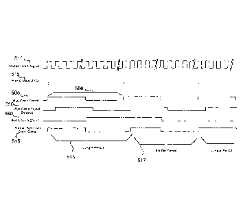
are split into two buckets is shown in Figure 5. At 505, the bus clock signal
is shown having
a period 506. The master clock signal 311, as discussed above, has a period
that is n times
shorter than the bus clock signal. The spread spectrum signal 515 is generated
by lengthening
14
CA 02816522 2013-05-23
and shortening the bus clock signal by one master clock signal period. For
instance, the
longer period 516 and the shorter period 517 may be expressed as:
[00070] Longer period = bus clock signal period + master clock signal
period
[00071] Shorter period = bus clock signal period ¨ master clock signal
period.
[00072] This may be achieved by delaying every other rising edge of the bus
clock
signal by one master clock signal period, as shown at 510, wherein a 1 means
delaying the
rising edge and a 0 means not delaying the rising edge. Those of skill in the
art will
appreciate a rising edge transition is used when devices utilizing the clock
for synchronization
are configured for rising edge transitions. If such devices were configured
for falling edge
transitions, similar results could be achieved by delaying every other falling
edge.
[00073] Figure 7 shows an example circuit 700 for performing the method
500,
configured in accordance with some implementations. It will be appreciated
that example
circuit 700 is only an example and that other implementations may be used to
achieve the
described functionalities. In some implementations, the example circuit 700 is
implemented
using a programmable logic device and the circuit may be specified using a
hardware design
language such as VHSIC hardware description language (VHDL) or Verilog. In
other
implementations, the example circuit or a circuit with similar function may be
implemented in
specialized hardware rather than the programmable logic device.
[00074] As shown in Figure 7, the circuit 700 is configured to receive the
bus clock
signal 505 and the master clock signal 311 and to output the spread spectrum
clock signal
515. For this example circuit 700, an assumption may be made that the master
clock signal
311 leads the bus clock signal 505 in order to avoid a race condition. This is
a reasonable
assumption when the master clock signal 311 is used to generate the bus clock
signal 505. If
this assumed timing relationship between the master clock signal 311 and the
bus clock signal
505 is not the case or if the relationship is unknown, the circuit that
generates the spread
spectrum clock signal 515 would have to take this in account to avoid a race
condition.
CA 02816522 2013-05-23
[00075] The bus clock signal delayed 550 is the bus clock signal delayed by
one master
clock period by a D flip flop 570 that clocks the bus clock signal 505 on
positive transitions of
the master clock signal 311.
[00076] The D flip flop 571 operates as a free-running divider that creates
the bus clock
signal/2 560 having half the frequency of the bus clock signal 505. The bus
clock signal/2
560 transitions on falling edges of the bus clock signal 505. It will be
appreciated that in
some implementations, the circuit 700 would be designed so that the state of
the D flip flop
571 would be controlled, and not be allowed to run free as in this example
circuit.
[00077] Combinatorial circuitry 572 generates the spread spectrum clock
signal 515
using the bus clock signal 505, the bus clock signal delayed 550 and the bus
clock signal/2
560. In this example, the combinatorial circuitry includes two AND gates and
an OR gate.
The spread spectrum clock signal 515 is generated by combining the inversion
of the bus
clock signal 505, the bus clock signal delayed 550, the bus clock signal/2
560, and the
inversion of the bus clock signal/2 560. The bus clock signal/2, operating at
half the
frequency of the bus clock signal, is used by the combinatory circuitry 572 to
alternately
select the bus clock signal, and on every other cycle, to select the ANDed
output of the bus
clock signal delayed 550 and bus clock signal 505.
[00078] An example of a digital spread spectrum technique where the EM
emissions
are split into three buckets is shown in Figure 6. The spread spectrum bus
clock 615 includes
the longer period 616, the shorter period 617, and .a normal period 606. This
can be achieved
by delaying one out of every three rising edges of the bus clock signal by one
master clock
signal period, as shown at 610, wherein a 1 means delaying the rising edge and
a 0 means not
delaying the rising edge. Those of skill in the art will appreciate that
similar digital
approaches can be used to achieve greater emission reduction by more
complicated delay
variations that cause the bus clock to modulate between more than three
frequencies.
[00079] Returning to Figure 4, the spread spectrum clock signal is sent to
the one or
more elements, such as the lighting boards 302, in block 415. The spread
spectrum clock
signal may be carried along the length 327 of the bus 325 along with the data
signal 317. In
some implementations, the data signal may be given the same timing treatment,
such as by the
16
CA 02816522 2013-05-23
programmable logic device, as the bus clock signal. This allows the data
signal to be
synchronized with the "jitter" of the spread spectrum clock signal to avoid
possible clock and
data synchronization problems at the one or more elements.
[00080] These and other aspects of the disclosure may be implemented by
various
types of hardware, software, firmware, etc. For example, some features of the
disclosure may
be implemented, at least in part, by machine-readable media that include
program
instructions, state information, etc., for performing various operations
described herein.
Examples of program instructions include both machine code, such as produced
by a
compiler, and files containing higher-level code that may be executed by the
computer using
an interpreter. Examples of machine-readable media include, but are not
limited to, magnetic
media such as hard disks, floppy disks, and magnetic tape; optical media such
as CD-ROM
disks; magneto-optical media; and hardware devices that are specially
configured to store and
perform program instructions, such as read-only memory devices ("ROM") and
random
access memory ("RAM").
[00081] Any of the above implementations may be used alone or together with
one
another in any combination. Although various implementations may have been
motivated by
various deficiencies with the prior art, which may be discussed or alluded to
in one or more
places in the specification, the implementations do not necessarily address
any of these
deficiencies. In other words, different implementations may address different
deficiencies
that may be discussed in the specification. Some implementations may only
partially address
some deficiencies or just one deficiency that may be discussed in the
specification, and some
implementations may not address any of these deficiencies.
[00082] While various implementations have been described herein, it should
be
understood that they have been presented by way of example only, and not
limitation. Thus,
the breadth and scope of the present application should not be limited by any
of the
implementations described herein, but should be defined only in accordance
with the
following and later-submitted claims and their equivalents.
[00083] It will be understood that unless features in any of the above-
described
implementations are expressly identified as incompatible with one another or
the surrounding
17
CA 02816522 2013-05-23
context implies that they are mutually exclusive and not readily combinable in
a
complementary and/or supportive sense, the totality of this disclosure
contemplates and
envisions that specific features of those implementations can be selectively
combined to
provide one or more comprehensive, but slightly different, technical
solutions. It will
therefore be further appreciated that the above description has been given by
way of example
only and that modifications in detail may be made within the scope of the
invention.
=
18