Note : Les descriptions sont présentées dans la langue officielle dans laquelle elles ont été soumises.
CA 02816840 2013-05-02
WO 2012/066273
PCT/GB2011/001579
1
METHOD FOR REDUCING CREEP CORROSION
The present invention relates to a method for reducing creep corrosion on
printed
circuit boards, to coated printed circuit boards and to the use of particular
polymers to
reduce creep corrosion.
BACKGROUND
Creep corrosion is a major problem in the electronics industry. Its increasing
impact
on the electronics industry is believed to be a result of a variety of
factors, such as
increased use of lead-free solder, miniaturization of components and exposure
of
electronic assemblies to increasingly harsh environments.
Creep corrosion is a mass transport process in which solid corrosion products,
typically metal sulfides, migrate over a surface. It is a particular problem
for printed
circuit boards, where corrosion products may migrate onto solder mask surfaces
on
the printed circuit boards. This can result in short circuits between adjacent
conductive tracks on the printed circuit boards and failure of the product.
The mechanism of creep corrosion is not well understood, but it is known to be
a
particular problem in high sulfur environments, where printed circuit boards
may fail
within six weeks. Moisture is also believed to be a contributory factor.
Various strategies for reducing creep corrosion have been attempted. Such
strategies
include: application of conformal coatings; cleaning of the printed circuit
board
following assembly; careful choice of the printed circuit board surface
finish; and
capping all non-soldered conductive tracks on the printed circuit board.
Each of these proposed solutions has been shown to fail in at least some cases
and can
actually make the situation worse. There is therefore a requirement in the
electronics
industry for a more reliable and efficient method for reducing creep
corrosion.
CA 02816840 2013-05-02
WO 2012/066273
PCT/GB2011/001579
2
SUMMARY OF THE INVENTION
The present inventors have surprisingly found that a plasma-polymerized
fluorohydrocarbon polymer can be used to reduce creep corrosion.
Thus, the present invention provides a method for reducing creep corrosion on
a
printed circuit board, the printed circuit board comprising a substrate, a
plurality of
electrically conductive tracks located on at least one surface of the
substrate, a solder
mask coating at least a first area of the plurality of electrically conductive
tracks and a
surface finish coating at least a second area of the plurality of electrically
conductive
tracks, the method comprising depositing by plasma-polymerization a
fluorohydrocarbon onto at least part of the solder mask and at least part of
the surface
finish.
The invention further provides a coated printed circuit board obtainable by
the method
of the invention.
The invention further provides a coated printed circuit board comprising a
substrate, a
plurality of electrically conductive tracks located on at least one surface of
the
substrate, a solder mask coating at least a first area of the plurality of
electrically
conductive tracks, a surface finish coating at least a second area of the
plurality of
electrically conductive tracks, and a plasma-polymerized fluorohydrocarbon
coating
on at least part of the solder mask and at least part of the surface finish.
The invention further provides use of a plasma-polymerized fluorohydrocarbon
to
reduce creep corrosion of a printed circuit board, the printed circuit board
comprising
a substrate, a plurality of electrically conductive tracks located on at least
one surface
of the substrate, a solder mask coating at least a first area of the plurality
of
electrically conductive tracks and a surface finish coating at least a second
area of the
plurality of electrically conductive tracks.
CA 02816840 2013-05-02
WO 2012/066273
PCT/GB2011/001579
3
DESCRIPTION OF THE FIGURES
Figure 1 shows a portion of the printed circuit board of Example 1, after 7
days of the
sulfur clay test. Very little creep corrosion is visible.
Figure 2 shows a portion of the printed circuit board of Example 2, after 7
days of the
sulfur clay test. Very little creep corrosion is visible.
Figure 3 shows a portion of the printed circuit board of Example 3, after 7
days of the
sulfur clay test. Very little creep corrosion is visible.
Figure 4 shows a portion of the printed circuit board of Example 4, after 7
days of the
sulfur clay test. Very little creep corrosion is visible.
Figure 5 shows a portion of the printed circuit board of Example 5, after 7
days of the
sulfur clay test. Very little creep corrosion is visible.
Figure 6 shows a portion of the printed circuit board of Example 6, after 7
days of the
sulfur clay test. No creep corrosion is visible.
Figure 7 shows a portion of the printed circuit board of Example 7, after 7
days of the
sulfur clay test. Very little creep corrosion is visible..
Figure 8 shows a portion of the printed circuit board of Comparative Example
1, after
7 days of the sulfur clay test. Extensive creep corrosion is visible.
Figure 9 shows a portion of the printed circuit board of Comparative Example
2, after
7 days of the sulfur clay test. Extensive creep corrosion is visible.
Figure 10 shows a portion of the printed circuit board of Comparative Example
3,
after 7 days of the sulfur clay test. Extensive creep corrosion is visible.
Figure 11 shows a portion of the printed circuit board of Comparative Example
4,
after 7 days of the sulfur clay test. Extensive creep corrosion is visible.
CA 02816840 2013-05-02
WO 2012/066273
PCT/GB2011/001579
4
Figure 12 shows a cross-section of an example of a printed circuit board prior
to
coating by the method of the invention.
Figure 13 shows a cross-section of an example of a coated printed circuit
board.
DETAILED DESCRIPTION OF THE INVENTION
An example method of the present invention involves depositing by plasma-
polymerization a plasma-polymerized fluorohydrocarbon onto a printed circuit
board
comprising a substrate, a plurality of electrically conductive tracks located
on at least
one surface of the substrate, a solder mask coating at least a first area of
the plurality
of electrically conductive tracks and a surface finish coating at least a
second area of
the plurality of electrically conductive tracks.
In particular, the example method may involve depositing the plasma-
polymerized
fluorohydrocarbon onto at least part of the solder mask, at least part of the
surface
finish and at least a third area of the plurality of electrically conductive
tracks which is
not coated with solder mask or surface finish.
Typically the plasma-polymerized fluorohydrocarbon is deposited onto more than
75%, and preferably more than 90%, of the surface area of the solder mask. The
plasma-polymerized fluorohydrocarbon may be deposited onto substantially all
of the
surface area of the solder mask
Typically the plasma-polymerized fluorohydrocarbon is deposited onto more than
75%, and preferably more than 90%, of the surface area of the surface finish.
The
plasma-polymerized fluorohydrocarbon may be deposited onto substantially all
of the
surface area of the surface finish.
The plurality of electrically conductive tracks may comprise a third area
which is not
coated with solder mask or surface finish. Such an area which is not coated
with
solder mask or surface finish is generally a defect, normally in the surface
finish or
solder mask. It is generally preferably for areas of the electrically
conductive tracks
CA 02816840 2013-05-02
WO 2012/066273
PCT/GB2011/001579
which are not coated with solder mask or surface finish to be absent. If a
third area of
plurality of electrically conductive tracks which is not coated with solder
mask or
surface finish is present, typically the plasma-polymerized fluorohydrocarbon
is
deposited onto at least part of the third area. Preferably the plasma-
polymerized
5 fluorohydrocarbon is deposited onto more than 75%, and more preferably
more than
90%, of the surface area of the plurality of electrically conductive tracks
which is not
coated with solder mask or surface finish or attached to the substrate. The
plasma-
polymerized fluorohydrocarbon may be deposited onto substantially all of the
surface
area of the plurality of electrically conductive tracks which is not coated
with solder
mask or surface finish or attached to the substrate.
Generally, the plasma-polymerized fluorohydrocarbon is also deposited onto to
at
least part of the substrate which is not covered by the plurality of
conductive tracks.
Typically the plasma-polymerized fluorohydrocarbon is deposited onto more than
75%, and preferably more than 90%, of the surface area of the substrate which
is not
covered by the plurality of conductive tracks.
Plasma-polymerized polymers are a unique class of polymers which cannot be
prepared by traditional polymerization methods. Plasma-polymerized polymers
have
a highly disordered structure and are generally highly crosslinked, contain
random
branching and retain some reactive sites. Plasma-polymerized polymers are thus
chemically distinct from polymers prepared by traditional polymerization
methods
known to those skilled in the art. These chemical and physical distinctions
are well
known and are described, for example in Plasma Polymer Films, Hynek Biederman,
Imperial College Press 2004.
A plasma-polymerized fluorohydrocarbon is typically a straight and/or branched
polymer which optionally contains cyclic moieties. Said cyclic moieties are
preferably alicyclic rings or aromatic rings, more preferably aromatic rings.
Preferably the plasma-polymerized fluorohydrocarbon does not contain any
cyclic
moieties. Preferably the plasma-polymerized fluorohydrocarbon is a branched
polymer.
CA 02816840 2013-05-02
WO 2012/066273
PCT/GB2011/001579
6
The plasma-polymerized fluorohydrocarbon optionally contains heteroatoms
selected
from N, 0, Si and P. Preferably, however, the plasma-polymerized
fluorohydrocarbon contains no N, 0, Si and P heteroatoms.
An oxygen-containing plasma-polymerized fluorohydrocarbon preferably comprises
carbonyl moieties, more preferably ester and/or amide moieties. A preferred
class of
oxygen-containing plasma-polymerized fluorohydrocarbon polymers are plasma-
polymerized fluoroacrylate polymers.
A nitrogen containing plasma-polymerized fluorohydrocarbon preferably
comprises
nitro, amine, amide, imidazole, diazole, trizole and/or tetraazole moieties
Preferably the plasma-polymerized fluorohydrocarbon is branched and contains
no
heteroatoms.
The plasma-polymerized fluorohydrocarbon used in the present invention may be
obtainable by a plasma-polymerization technique. Plasma-polymerization is
generally
an effective technique for depositing thin film coatings. Generally plasma-
polymerization provides excellent quality coatings, because the polymerization
reactions occur in situ. As a result, the plasma-polymerized polymer is
generally.
deposited in small recesses, under components and in vias that would not be
accessible by normal liquid coating techniques in certain situations.
Plasma deposition may be carried out in a reactor that generates a gas plasma
which
comprises ionised gaseous ions, electrons, atoms, and/or neutral species. A
reactor
may comprise a chamber, a vacuum system, and one or more energy sources,
although any suitable type of reactor configured to generate a gas plasma may
be
used. The energy source may include any suitable device configured to convert
one
or more materials to a gas plasma. Preferably the energy source comprises a
heater,
radio frequency (RF) generator, and/or microwave generator.
In an example method of the invention, a printed circuit board may be placed
in the
chamber of a reactor and a vacuum system may be used to pump the chamber down
to
pressures in the range of 10-3 to 10 mbar. One or more materials may then be
pumped
CA 02816840 2013-05-02
WO 2012/066273
PCT/GB2011/001579
7
into the chamber and an energy source may generate a stable gas plasma. One or
more precursor compounds may then be introduced, as gases and/or liquids, into
the
gas plasma in the chamber. When introduced into the gas plasma, the precursor
compounds may be ionized and/or decomposed to generate a range of active
species
in the plasma that polymerize to generate the polymer coating. Pulsed plasma
systems
may also be used.
A plasma-polymerized fluorohydrocarbon is preferably obtained by plasma
polymerization of one or more precursor compounds which are hydrocarbon
materials
comprising fluorine atoms. Preferred hydrocarbon materials comprising fluorine
atoms are perfluoroalkanes, perfluoroalkenes, perfluoroallcynes,
fluoroalkanes,
fluoroalkenes, fluoroalkynes. Examples include CF4, C2F4, C2F6, C3F6 C3F8and
C4F8.
The exact nature and composition of the plasma-polymerized fluorohydrocarbon
coating typically depends on one or more of the following conditions (i) the
plasma
gas selected; (ii) the particular precursor compound(s) used; (iii) the amount
of
precursor compound(s) (which may be determined by the combination of the
pressure
of precursor compound(s) and the flow rate); (iv) the ratio of precursor
compound(s);
(v) the sequence of precursor compound(s); (vi) the plasma pressure; (vii) the
plasma
drive frequency; (viii) the pulse width timing; (ix) the coating time; (x) the
plasma
power (including the peak and/or average plasma power); (xi) the chamber
electrode
arrangement; and/or (xii) the preparation of the incoming assembly.
Typically the plasma drive frequency is 1 kHz to 1 GHz. Typically the plasma
power
is 500 to 10000 W. Typically the mass flow rate is 5 to 2000 sccm. Typically
the
operating pressure is 10 to 500 mTorr. Typically the coating time is 10
seconds to 20
minutes.
However, as a skilled person will appreciate, the preferred conditions will be
dependent on the size and geometry of the plasma chamber. Thus, depending on
the
specific plasma chamber that is being used, it may be beneficial for the
skilled person
to modify the operating conditions.
CA 02816840 2013-05-02
WO 2012/066273
PCT/GB2011/001579
8
The plasma-polymerized fluorohydrocarbon coating used in the present invention
typically has a mean-average thickness of 1 nm to 10 pm, preferably 1 mn to 5
pm,
more preferably 5nm to 500 nm, more preferably 10 nm to 100 nm, and more
preferably 25 nm to 75 nm, for example about 50 nm. The thickness of the
coating
may be substantially uniform or may vary from point to point.
The printed circuit board coated in the method of the present invention
comprises a
substrate, a plurality of electrically conductive tracks located on at least
one surface of
the substrate, a solder mask coating at least a first area of the plurality of
electrically
conductive tracks and a surface finish coating at least a second area of the
plurality of
electrically conductive tracks. The printed circuit boards generally do not
initially
have any electrical components attached thereto.
A person skilled in the art can select suitable shapes and configurations for
the
plurality of electrically conductive tracks, depending on the end-purpose of
the
printed circuit board. Typically, an electrically conductive track is attached
to the
surface of the substrate along its entire length. Alternatively, an
electrically
conductive track may be attached to the substrate at two or more points. For
example,
an electrically conductive track may be a copper wire attached to the
substrate at two
or more points, but not along its entire length.
An electrically conductive track is typically formed on a substrate using any
suitable
method known to those skilled in the art. In a preferred method, electrically
conductive tracks are formed on a substrate using a "subtractive" technique.
Typically in this method, a layer of electrically conductive material is
bonded to a
surface of the substrate and then the unwanted portions of the electrically
conductive
material are removed, leaving the desired conductive tracks. The unwanted
portions of
the electrically conductive material are typically removed from the substrate
by
chemical etching, photo-etching and/or milling. In an alternative method,
electrically
conductive tracks are formed on the substrate using an "additive" technique
such as,
for example, electroplating, deposition using a reverse mask, and/or any
geometrically
controlled deposition process.
CA 02816840 2013-05-02
WO 2012/066273
PCT/GB2011/001579
9
An electrically conductive track typically comprises gold, tungsten, copper,
silver
and/or aluminium, preferably gold, tungsten, copper, silver and/or aluminium,
more
preferably copper. An electrically conductive track may consist essentially or
consist
of copper.
The substrate of the printed circuit board generally comprises an electrically
insulating material. The substrate typically comprises any suitable insulating
material
that prevents the substrate from shorting the circuit of the printed circuit
board.
A substrate preferably comprises an epoxy laminate material, a synthetic resin
bonded
paper, an epoxy resin bonded glass fabric (ERBGH), a composite epoxy material
(CEM), PTFE (Teflon), or other polymer materials, phenolic cotton paper,
silicon,
glass, ceramic, paper, cardboard, natural and/or synthetic wood based
materials,
and/or other suitable textiles. The substrate optionally further comprises a
flame
retardant material, typically Flame Retardant 2 (FR-2) and/or Flame Retardant
4 (FR-
4). The substrate may comprise a single layer of an insulating material or
multiple
layers of the same or different insulating materials.
A solder mask may coat at least a first area of the electrically conductive
tracks. A
solder mask is generally intended to prevent solder from bridging the
electrically
conductive tracks, thereby preventing short circuits. Typically the solder
mask is an
epoxy solder mask, a liquid photoimageable solder mask (LPSM) ink or a dry
film
photoimageable solder mask (DFSM). Such solder masks can readily be applied to
the printed circuit board by techniques known to those skilled in the art.
Preferably the solder mask coating at least a first area of the plurality of
electrically
conductive tracks additionally coats an area of the substrate. In that case,
the solder
mask may overhang the edge of at least part of the electrically conductive
tracks and
covers an adjacent area of the substrate. Creep corrosion is generally
particularly
aggressive in this situation. Preferably, the plasma-polymerized
fluorohydrocarbon is
deposited onto the portion of the solder mask that additionally coats an area
of the
substrate or overhangs the edge of at least part of the electrically
conductive tracks
and covers an adjacent area of the substrate.
CA 02816840 2013-05-02
WO 2012/066273
PCT/GB2011/001579
A surface finish may coat at least a second area of the electrically
conductive tracks.
The surface finish is typically immersion silver (ImAg), electroless
nickel/immersion
gold (ENIG), organic solderability preservative (OSP), electroless
nickel/electroless
palladium/immersion gold (ENEPIG) or immersion tin (ImSn). Preferably the
surface
5 finish is immersion silver (ImAg) or organic solderability preservative
(OSP), more
preferably immersion silver (ImAg).
Optionally, an example method of the invention may additionally comprise,
after
deposition of the plasma-polymerized fluorohydrocarbon, connecting at least
one
10 electrical component to at least one electrically conductive track. The
at least one
electrical component may be connected to the at least one conductive track
through
the plasma polymerised fluorohydrocarbon.
Preferably, the electrical component is connected to the at least one
electrically
conductive track via a solder joint, a weld joint or a wire-bond joint. If the
electrical
component has been connected through the plasma polymerized fluorohydrocarbon,
preferably the solder joint, weld joint or wire-bond joint abuts the plasma
polymerised
fluorohydrocarbon. It is possible to solder, weld or wire bond through the
plasma
polymerized fluorohydrocarbon, as described in WO 2008/102113 (the content of
which is incorporated herein by reference).
An electrical component may be any suitable circuit element of printed circuit
board.
Preferably, an electrical component is a resistor, capacitor, transistor,
diode, amplifier,
antenna or oscillator. Any suitable number and/or combination of electrical
components may be connected to the electrical assembly.
After the coated printed circuit board has been assembled, that is to say all
necessary
electrical components have been connected, it may be desired to deposit by
plasma-
polymerization an additional coating of plasma-polymerized fluorohydrocarbon.
The
additional coating may be a conformal coating. This can generally provide
additional
environmental and physical protection.
The present invention also relates to a coated printed circuit board. Example
coated
printed circuit boards may be prepared methods described above. Such coated
printed
CA 02816840 2013-05-02
WO 2012/066273
PCT/GB2011/001579
11
circuit boards may comprise a substrate, a plurality of electrically
conductive tracks
located on at least one surface of the substrate, a solder mask coating at
least a first
area of the plurality of electrically conductive tracks, a surface finish
coating at least a
second area of the plurality of electrically conductive tracks, and a plasma-
polymerized fluorohydrocarbon coating on at least part of the solder mask, at
least
part of the surface finish and optionally at least a third area of the
plurality of
electrically conductive tracks which is not coated with solder mask or surface
finish.
The substrate, electrically conductive tracks, solder mask, surface finish and
plasma-
polymerized fluorohydrocarbon may be as defined above.
Example coated printed circuit boards may further comprise an electrical
component
connected to at least one electrically conductive track through the plasma-
polymerized fluorohydrocarbon coating. The electrical component and connection
to
the electrically conductive track may be as defined above.
The present invention also relates to use of a plasma-polymerized
fluorohydrocarbon
to reduce creep corrosion of a printed circuit board which may be as defined
above.
Aspects of the invention will now be described with reference to the
embodiment
shown in Figures 12 and 13, in which like reference numerals refer to the same
or
similar components.
Figure 12 shows an example of printed circuit board prior to coating
comprising a
substrate 1, a plurality of electrically conductive tracks 2 located on at
least one
surface 3 of the substrate, a solder mask 4 coating at least a first area 5 of
the plurality
of electrically conductive tracks and a surface finish 6 coating at least a
second area 7
of the plurality of electrically conductive tracks. The solder mask optionally
additionally coats an area 8 of the substrate.
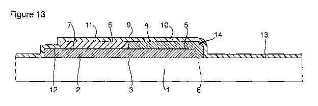
Figure 13 shows an example of a coated printed circuit board comprising a
substrate
1, a plurality of electrically conductive tracks 2 located on at least one
surface 3 of the
substrate, a solder mask 4 coating at least a first area 5 of the plurality of
electrically
conductive tracks, a surface finish 6 coating at least a second area 7 of the
plurality of
electrically conductive tracks, and a plasma-polymerized fluorohydrocarbon
coating 9
CA 02816840 2013-05-02
WO 2012/066273
PCT/GB2011/001579
12
on at least part 10 of the solder mask, at least part 11 of the surface finish
and
optionally at least a third area 12 of the plurality of electrically
conductive tracks
which is not coated with solder mask or surface finish. The plasma-polymerized
fluorohydrocarbon also optionally coats at least part 13 of the substrate.
Aspects of the invention will now be described with reference to the Examples
EXAMPLES
Sulfur clay test method
The sulfur clay test method is a technique for simulating conditions, such as
a clay
modelling studio, where creep corrosion is very aggressive. This method is a
well-
known technique in the art for assessing the effects of creep corrosion and
uses a
sulfur bearing clay as a source of sulfur compounds (see, for example, Creep
corrosion on lead-free printed circuit boards in high sulfur environments,
Randy
Schueller, Published in SMTA Int '1 Proceedings, Orlando, FL, Oct 2007).
Plasteline sulphur bearing modelling clay (marketed by Chavant) was wetted
with
water and heated inside a container. Test printed circuit boards were
immediately
placed in the container with the hot clay. Sulfur compounds from the clay
condensed
onto the surfaces of the printed circuit boards and created suitable
conditions for creep
corrosion.
Coating A
A printed circuit board was introduced to a plasma chamber. The chamber was
pumped down to an operating pressure of 50 mTorr and C3F6 gas was introduced
at a
flow rate of 100 sccm. The gas was allowed to flow through the chamber for 30
seconds and then the plasma generator was switched on at a frequency of
13.56MHz
and a power of 2.4 kW. The printed circuit board was exposed to the active
plasma for
a time period of 7 minutes, after which the plasma generator was switched off,
the
chamber brought back to atmospheric pressure, and the coated printed circuit
board
removed from the chamber.
CA 02816840 2013-05-02
WO 2012/066273
PCT/GB2011/001579
13
Coating B
A printed circuit board was introduced to a plasma chamber. The chamber was
pumped down to an operating pressure of 70 mTorr and C3F6 gas was introduced
at a
flow rate of 750 sccm. The gas was allowed to flow through the chamber for 30
seconds and then the plasma generator was switched on at a frequency of 40 KHz
and
a power of 7 kW. The printed circuit board was exposed to the active plasma
for a
time period of 10 minutes, after which the plasma generator was switched off,
the
chamber brought back to atmospheric pressure, and the coated printed circuit
board
removed from the chamber.
Coating C
A printed circuit board was introduced to a plasma chamber. The chamber was
pumped down to an operating pressure of 60 mTorr and C3F6 gas was introduced
at a
flow rate of 750 sccm. A second gas, helium, was added to the chamber at a
flow rate
of 100 scorn through a second mass flow controller. The gas mixture was
allowed to
flow through the chamber for 30 seconds and then the plasma generator was
switched
on at a frequency of 40 KHz and a power of 7 kW. The printed circuit board was
exposed to the active plasma for a time period of 10 minutes, after which the
plasma
generator was switched off, the chamber brought back to atmospheric pressure,
and
the coated printed circuit board removed from the chamber.
Evaluation of test printed circuit boards
Starting from standard blank printed circuit boards with copper tracks and
solder
mask, a series of test printed circuit boards were prepared. These had the
features set
out in Tables 1 and 2 below.
In particular, a surface finish of immersion silver (ImAg) or organic
solderability
preservative (OSP) was optionally applied to each printed circuit board.
Coating A
was then optionally deposited onto the printed circuit board. Next, electrical
components were optionally connected to the printed circuit board. Finally, an
CA 02816840 2013-05-02
WO 2012/066273
PCT/GB2011/001579
14
overcoat of Coating A, Coating B or Coating C was optionally applied over the
printed circuit board and electrical components.
Example I Surface Creep corrosion Components Overcoat Evaluation
finish reduction coating in situ
1 No Coating A No No
2 No Coating A Yes No
3 No Coating A Yes Coating A +
4 ImAg Coating A Yes No
No Coating A Yes Coating B +
6 No Coating A Yes Coating C
7 OSP Coating A Yes No
5 TABLE 1
Comparative Surface Creep Components Overcoat Evaluation
Example finish corrosion in situ
reduction
coating
1 ImAg No No No
2 ImAg No Yes No
3 ImAg No Yes Coating A --
4 OSP No Yes No
TABLE 2
The printed circuit boards of Examples 1 to 7 and Comparative Examples 1 to 4
were
subjected to the sulfur clay test for 7 days. After 7 days, the printed
circuit boards
were removed and examined for the presence of creep corrosion.
Figures 1 to 11 show equivalent portions of the printed circuit boards of
Example 1 to
7 and Comparative Examples 1 to 4 respectively. As shown in Tables 1 and 2,
the
printed circuit boards were categorised as follows:
No creep corrosion (++)
CA 02816840 2013-05-02
WO 2012/066273
PCT/GB2011/001579
Low levels creep corrosion (+)
High levels of creep corrosion (--)
Conclusions
5
The application by plasma-polymerization of a fluorohydrocarbon onto a printed
circuit board prior to addition of electronic components significantly reduced
the
incidence of creep corrosion.