Note : Les descriptions sont présentées dans la langue officielle dans laquelle elles ont été soumises.
CA 02821707 2013-06-13
SPECIFICATION
Title of Invention
LINE LIGHT IRRADIATION DEVICE
Technical Field
[0001]
Background Art
[0002]
In recent years, there have been many integrated circuits which are
low-voltage driven and an output voltage required for a switching power
supply device is also being lowered in voltage. As a result, a specification
of
a power supply device has a tendency to be lower in voltage but larger in
current, and in order to suppress an electric resistance of not only an output
circuit of the power supply device but also each current path inside the power
supply device, a bus bar (power-feeding member) is used as a conductive
member having a necessary but not a sufficient cross-section area, as shown
in Patent Literature 1.
[0003]
And the present applicant considers to provide a bus bar on each
LED wiring substrate in a line light irradiation device having a plurality of
substantially long sized LED wiring substrates and a casing for
accommodating the LED wiring substrates. It is noted that, in an LED
wiring substrate without using a bus bar, since a width of the LED wiring
substrate is restricted to an accommodation width of a casing, the
power-feeding line becomes thin and there may arise a problem that the line
may be burned and disconnected in the case where required electric capacity
1
CA 02821707 2013-06-13
becomes larger.
[0004]
Conventionally, connection of bas bars provided on the LED wiring
substrates is performed by co-fastening the end portions of the bus bars of
the adjacent LED wiring substrates with screw members via a connection
plate (for example, copper plate) having conductivity at each end portion.
[0005]
However, in a structure of co-fastening with screw members, there is
a problem that the number of parts such as connection plate and screw
member etc. is increased and the number of assembling man-hours is
increased. Further, in a configuration that the end portions of the bus bar
of the adjacent LED wiring substrates are connected to each other via the
connection plate, there is a problem that the connection becomes difficult in
the case where a position of a screw hole formed in the bus bar and a position
of a screw hole of the connection plate are displaced at the time of
connection,
the connection becomes difficult. In the assembly of connecting the
connection plate to the bus bar after fixing the LED wiring substrate to the
casing, there is a problem that a working space for connecting the bus bar is
narrow and workability becomes extremely bad.
Citation List
Patent Literature
[0006]
Patent Literature I: JP-A2000-252664
Summary of Invention
Technical Problem
2
CA 02821707 2013-06-13
[0007]
Therefore, the present invention has been made in order to solve the
above problem at a stroke and a main expected object thereof is to allow to
make a width of an LED wiring substrate compact and to reduce the number
of assembly parts and assembly man-hours.
Solution to Problem
[0008]
That is, a line light irradiation device according to the present
invention is a light irradiation device comprising a plurality of
substantially
long-sized LED wiring substrates arranged in a longitudinal direction, each
of the LED wiring substrates including: a plurality of LEDs provided in a
line shape along the longitudinal direction; and power-feeding line members
provided in parallel with an arrangement direction of the plurality of LEDs
for supplying electric power to the plurality of LEDs, wherein the
power-feeding line members are provided above an LED mounting surface of
each of the LED wiring substrates, and in the adjacent LED wiring
substrates, the power-feeding line members provided in one of the adjacent
LED wiring substrates include contact terminals provided to extend outward
in the longitudinal direction and contact with the power-feeding line
members of the other LED wiring substrate. Here, the phrase "provided to
extend outward in the longitudinal direction" means that the contact
terminals are protruding outward the LED wiring substrate in plan view.
[0009]
With a configuration like this, since the power-feeding line member is
provided above the LED mounting surface, the power-feeding line member
3
CA 02821707 2013-06-13
_
can be made thick in accordance with a required electric capacity
irrespective of a width of the LED wiring substrate, and the width of the
LED wiring substrate can be made compact. In addition, since the contact
terminals provided in the power-feeding line members provided in one of the
adjacent LED wiring substrates contact with the power-feeding line
members of the other LED wiring substrate, parts of a connection plate and
a screw member required for a co-fastening structure can be made
unnecessary, and the number of parts can be reduced. Further, since the
power-feeding line members of the adjacent LED wiring substrates are
electrically connected to each other by the contact terminals, the number of
assembling man-hours can be also reduced.
[0010]
It is desirable that the contact terminals are integrally formed with
the power-feeding line members and elastically deformed to be pressed in
contact with the power-feeding line members of the adjacent LED wiring
substrate. With this, since the power-feeding line members and the contact
terminals are integrally formed, the number of parts of the LED wiring
substrate can be reduced and the number of assembling man-hours of the
LED wiring substrate can be also reduced. Further, since the contact
terminals are elastically deformed to be pressed in contact with the
power-feeding line members, the electric contact between the power-feeding
line members of the adjacent LED wiring substrates can be surely
performed.
[0011]
It is desirable to provide a casing having a bottom wall part
4
CA 02821707 2013-06-13
extending in the longitudinal direction and a pair of left and right side wall
parts extending upward from both sides in the longitudinal direction of the
bottom wall part, with the plurality of LED wiring substrates being arranged
on the bottom wall part, wherein, by fixing the plurality of LED wiring
substrates to the bottom wall part, the contact terminals are elastically
deformed to be pressed in contact with upper surfaces of the power-feeding
line members of the adjacent LED wiring substrate. With this, at the same
time of fixing the LED wiring substrate to the bottom wall part, a power
caused by the fixing can be effectively used and the contact terminals can be
surely brought into contact with the power-feeding line members of the
adjacent LED wiring substrate.
[0012]
It is desirable that one of the pair of power-feeding line members has
the contact terminal at one end part in the longitudinal direction and the
other of the pair of power-feeding line members has the contact terminal at
the other end part in the longitudinal direction. With this, the structure of
each LED wiring substrate can be commonly shared and the number of parts
can be reduced. Further, since a reaction force (force leaving from the
bottom wall part) received by pressing one of the power-feeding line
members in contact with the power-feeding line member of the adjacent LED
wiring substrate and a force (force toward the bottom wall part) which the
other power-feeding line members receive from the contact terminals of the
power-feeding line members of the adjacent LED wiring substrate counteract
as cancelling each other, the LED wiring substrate can be stably fixed.
[0013]
CA 02821707 2013-06-13
,.
=
Further, it may be also considered that each of the pair of
power-feeding line members has the contact terminal at one end part in the
longitudinal direction. With this, the structure of each LED wiring
substrate can be commonly shared and the number of parts can be reduced,
and in the case where some of the plurality of LED wiring substrates
accommodated in the casing are exchanged, it can be made easy to exchange.
[0014]
In order to effectively use both sides of the plurality of LEDs to be
able to withstand larger current in the LED wiring substrate, it is desirable
that the power-feeding line members are paired so as to interpose the
plurality of LEDs therebetween.
[0015]
It is desirable that the power-feeding line members are fixed with
screws to a surface implementing spacer soldered to the LED mounting
surface of the LED wiring substrate. With this, the power-feeding line
members can be made detachable with respect to the LED wiring substrate
and the power-feeding line members can be variously exchanged.
Advantageous Effects of Invention
[0016]
According to the present invention like this, the width of the LED
wiring substrate can be made compact and the number of assembly parts
and number of assembling man-hours can be reduced.
Brief Description of Drawings
[0017]
[Fig. 1] Fig. 1 is a perspective view showing a line light irradiation
6
CA 02821707 2013-06-13
device of the present embodiment.
[Fig. 21 Fig. 2 is a cross sectional view of the line light irradiation
device of the same embodiment.
[Fig. 31 Fig. 3 is a partially expanded sectional view showing details
of a fixing mechanism of the same embodiment.
[Fig. 4] Fig. 4 is a cross sectional view of an LED wiring substrate of
the same embodiment.
[Fig. 51 Fig. 5 is a side view of the LED wiring substrate of the same
embodiment.
[Fig. 6] Fig. 6 is a plan view of the LED wiring substrate of the same
embodiment.
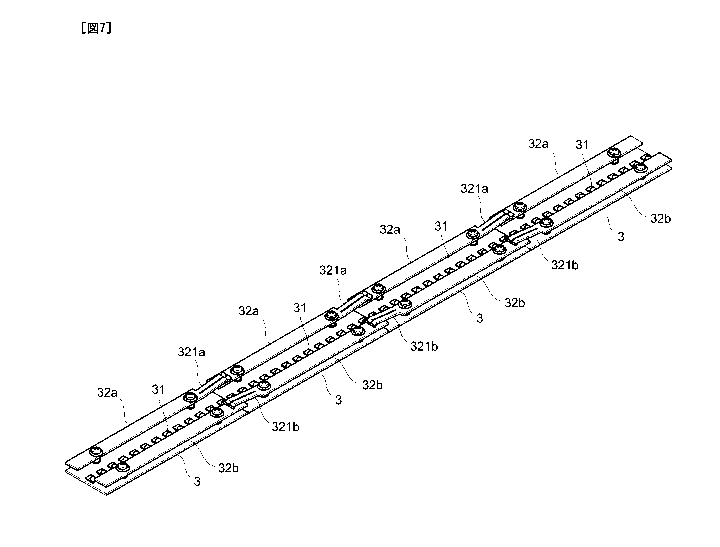
[Fig. 7] Fig. 7 is a perspective view of the LED wiring substrate of the
same embodiment.
[Fig. 81 Fig. 8 is a plan view showing a modification of an LED wiring
substrate.
[Fig. 91 Fig. 9 is a plan view showing a modification of the LED
wiring substrate.
[Fig. 101 Fig. 10 is a plan view showing a modification of the LED
wiring substrate.
[Fig. 11] Fig. 11 is a plan view showing a modification of the LED
wiring substrate.
[Fig. 121 Fig. 12 is a schematic diagram showing a modification of a
contact terminal.
[Fig. 13] Fig. 13 is a side view showing a modification of the LED
wiring substrate.
7
CA 02821707 2013-06-13
[Fig. 14] Fig. 14 is a side view showing a modification of the LED
wiring substrate.
Reference Signs List
[0018]
100 ... Line light irradiation device
2 ... Casing
21 ... Bottom wall part
22, 23 ... Side wall part
3 ... LED wiring substrate
31 ...LED
3b ... LED mounting surface
32a, 32b ... Power-feeding line member
321a, 321b ... Contact terminal
33 ...Surface implementing spacer
Description of Embodiments
[0019]
Next, one embodiment of a line light irradiation device 100 according
to the present invention is described referring to drawings.
[0020]
The line light irradiation device 100 according to the present
embodiment is adapted to irradiate line shaped light to, for example, a
predetermined irradiation region of an inspection object (work) and it is used
for such as a product inspection system etc. which photographs the
predetermined irradiation region with a photographing device (not shown),
captures obtained image data with an image processing device (not shown) to
8
CA 02821707 2013-06-13
perform an automatic inspection of checking presence or absence of a defect
such as, e.g., a crack or dirt, a foreign matter in liquid, or mark
inspection.
[0021]
Specifically, as shown in Figs. 1 and 2, this device is provided with: a
casing 2; a LED substrate 3 accommodated in the casing 2; a rod lens 4
which is a rod-like lens accommodated in the casing 2; and a fixing
mechanism 5 for fixing the rod lens 4 to the casing 2.
[0022]
As shown in Fig. 2, the casing 2 is adapted to accommodate the LED
substrate 3, rod lens 4 and a light transmission plate 6 such as a diffusion
plate and a protection cover. Specifically, the casing 2 is long sized metal
one and is formed in a generally U-character shape in section
perpendicularly intersecting in a longitudinal direction (extending
direction),
and includes a bottom wall part 21 extending in the longitudinal direction
and a pair of left and right side wall parts 22 and 23 extending upward from
longitudinal-directed both sides of this bottom wall part 21. This casing 2 is
integrally formed one by extrusion molding or pultrusion molding, and on a
back surface of the bottom wall part 21, there are provided plural sheets of
radiator fins F along the longitudinal direction for radiating heat to the
outside from the LED substrate 3. Further, in the bottom wall part 21, and
left and right side wall parts 22 and 23, there are provided attachment
grooves 2M for attaching the line light irradiation device 100 to an external
member (e.g., rack etc.). Further, front and rear side walls 24 and 25 are
fixed to one end and the other end in the longitudinal direction of the casing
2 with screws and the like. Thus, the casing 2 is formed with a generally
9
CA 02821707 2013-06-13
rectangular shaped light outgoing port 2H in the upper part thereof. In
addition, an electrical cable 8 is extended from the rear side wall 25 for
supplying electric power to the LED.
[00231
The LED substrate 3 is a long sized substrate mounting a plurality of
LEDs 31. Specifically, the LED substrate 3 is formed by machine-mounting
the plurality of LEDs 31 to be arranged in one or more lines (one line in Fig.
2) in a shorted side direction on a surface of a long sized print circuit
substrate so as to align optical axes Cl thereof in a generally constant
direction to be in a straight line state in a longer side direction. The LEDs
31 are surface mount typed ones of arranging LED elements in a center of a
package which forms, for example, a thin rectangular plate shape. Such
LEDs 31 are arranged so as to arrange the LED elements, for example, at
predetermined intervals in the longer side direction and shorter side
direction, respectively.
[00241
This LED substrate 3 is fixed to an upper surface of the bottom wall
part 21 of the casing 2. And regarding this LED substrate 3, a longer side
direction side surface 3a of the LED substrate 3 contacts with a substrate
contacting surface 211 which is a substrate positioning structure provided
along the longitudinal direction on the bottom wall part 21, and the LED
substrate 3 is thereby positioned to the casing 2 in a lateral direction (a
direction perpendicular to the longitudinal direction).
[00251
The rod lens 4 is a condenser lens of a generally circular shape with
CA 02821707 2013-06-13
_
an equal cross-section having a generally same length as a length of each of
the left and right side walls 22 and 23 of the casing 2. This rod lens 4 is
provided along the longitudinal direction above the LED substrate 3 inside
the casing 2 and is fixed to be in a predetermined position with respect to
the
plurality of LEDs 31 mounted on the LED substrate 3 by a fixing mechanism
to be described later. Specifically, the rod lens 4 is fixed by the
fixing
mechanism 5 in a manner such that an optical axis C2 of the rod lens 4
coincides with the optical axes Cl of the plurality of LEDs 31 and that the
rod lens 4 is spaced a predetermined distance with respect to the plurality of
LEDs 31. In addition, the light transmission plate 6 such as a diffusion
plate and a protection cover is provided in a front (upper portion) in a light
outgoing side of the rod lens 4, and since this light transmission plate 6 is
thermally expanded, it is attached by a slide groove 7 with a slight play
formed in an inner surface of each of the left and right side walls 22 and 23.
[0026]
As shown in Fig. 3, the fixing mechanism 5 is intended to fix the rod
lens 4 to the pair of left and right side wall parts 22 and 23 of the casing
2,
and it includes a projected rim part 51 provided along the longitudinal
direction in an inner surface of each of the left and right side wall parts 22
and 23, two notch portions 52 provided along the longitudinal direction in
side peripheral surfaces of the rod lens 4, a concave groove 53 provided along
the longitudinal direction above the projected rim part 51 in the inner
surface of each of the left and right side wall parts 22 and 23, and an
elastic
body 54 detachably provided in each of the concave grooves 53.
[0027]
11
CA 02821707 2013-06-13
4
Especially, as shown in Fig. 3, each projected rim part 51 is provided
to be projected inward from the inner surface and extending over from one
end to the other end in the longitudinal direction of each of the left and
right
side wall parts 22 and 23, and it includes an upward surface 51a which is a
generally horizontal plane and an inward surface 51b which is a plane
generally perpendicular to the upward surface 51a. Further, the two
projected rim parts 51 provided in the respective left and right side wall
parts 22 and 23 have the same shape laterally symmetrical with respect to
the optical axis C2. In addition, a distance between the upper side portions
above the projected rim parts 51 in the pair of left and right side wall parts
22 and 23 is configured to be larger than the outer diameter of the rod lens 4
and configured to be able to accommodate the rod lens 4 from an upper
opening of the casing 2. Thus, the accommodating work of the rod lens 4
into the casing 2 is facilitated.
[0028]
Especially, as shown in Fig. 3, each notch potion 52 is formed to
extend over from one end to the other end in the longitudinal direction in
each of the side peripheral surfaces of the rod lens 4, and it includes a
downward surface 52a which is a plane contacting with the upward surface
51a of the projected rim part 51 and an outward surface 52b which is a plane
generally perpendicular to the downward surface 52a. The two notch
portions 52 formed in the rod lens 4 have the same shape laterally
symmetrical with respect to the optical axis C2.
[0029]
And a distance between the inward surfaces 51b of the two projected
12
CA 02821707 2013-06-13
rim parts 51 is generally identical to the distance between the outward
surfaces 52b of the two notch portions 52, and the inward surfaces 51b of the
projected rim parts 51 are in contact with the outward surfaces 52b of the
notch portions 52 in a state that the upward surfaces 51a of the projected rim
parts 51 are in contact with the downward surfaces 52a of the notch portions
52. Thus, the rod lens 4 can be positioned with respect to the casing 2 in the
vertical direction as well as in the horizontal direction. That is, the
optical
axis Cl of each LED 31 on the LED substrate 3 positioned in the lateral
direction with respect to the casing 2 coincides with the optical axis C2 of
the
rod lens 4 positioned in the lateral direction with respect to the casing 2.
[0030]
The concave groove 53 is provided along the longitudinal direction
above the projected rim part 51 to extend over from one end to the other end
in the longitudinal direction in the inner surface of each of the left and
right
side wall parts 22 and 23. This concave groove 53 is formed in a manner
such that the elastic body 54 is fit thereto in a state that the downward
surface 52a of the notch portion 52 is in contact with the upward surface 51a
of the projected rim part 51 and is formed in a position where the elastic
body
54 contacts with the side peripheral surface of the rod lens 4.
[0031]
The elastic body 54 is a linear tube having flexibility which is
detachably provided in the concave groove 53 and which is a silicon tube
excellent in heat resistance and corrosion resistance in the present
embodiment. This elastic body is fit to the concave groove 53 in a state that
the downward surface 52a of the notch portion 52 is in contact with the
13
CA 02821707 2013-06-13
,
upward surface 51a of the projected rim part 51 and is brought into contact
with the side peripheral surface of the upper side portion above the notch 52
in the rod lens 4 to thereby press the notch portion 52 to the projected rim
part 51.
[0032]
Thus, the plurality of LED wiring substrates 3 of the present
embodiment are arranged in the longitudinal direction on an upper surface
of the bottom wall part 21 of the casing 2, and as shown in Figs. 4 to 7, the
plurality of LED wiring substrates 3 are provided in parallel with an
arrangement direction of the plurality of LEDs 31 so as to interpose the
plurality of LEDs 31 therebetween provided in a line shape along the
longitudinal direction and have a pair of power-feeding line members 32a
and 32b for supplying electric power to the plurality of LEDs 31.
[00331
The pair of power-feeding line members 32a and 32b are provided
above an LED mounting surface (upper surface 3b of the wiring substrate) of
the LED wiring substrate 3 so as to be separated from the LED mounting
surface 3b, and each of the power-feeding line members 32a and 32b is
formed to have a long-sized shape provided along each of the longitudinal
side surfaces of the LED wiring substrate 3.
[00341
As shown in Figs. 5 and 6, each of the power-feeding line members
32a and 32b is formed of a conductive member such as, for example, copper
plate and is fixed with screws to surface implementing spacers 33 soldered to
the LED mounting surface 3b of the LED wiring substrate 3. It is noted
14
CA 02821707 2013-06-13
_
that the pair of power-feeding line members 32a and 32b are electrically
connected to a pattern wiring (not shown) provided on the LED wiring
substrate 3 via the surface implementing spacers 33.
[0035]
In addition, each of the power-feeding line members 32a and 32b is
arranged between the longitudinal side surface of the LED wiring substrate
3 and the LEDs 31 in a transverse direction in plan view (see Figs. 4 and 6).
Thus, it is possible to prevent a problem that the power-feeding line
members 32a and 32b come into contact with the left and right side wall
parts 22 and 23 to make the assembling work difficult at the time of
accommodating the LED wiring substrate 3 in the casing 2. More
preferably, the power-feeding line members 32a and 32b are arranged so as
not to interrupt the light directly incident to the rod lens 4 from the LEDs
31.
Thus, a light quantity loss of the LEDs 31 due to the power-feeding line
members 32a and 32b can be prevented.
[0036]
And as shown in Figs. 5 to 7, the power-feeding line member 32a
(upper side power-feeding line member in Fig. 6) which is one of the two
power-feeding line members 32a and 32b provided on each LED wiring
substrate 3 includes contact terminals 321a each of which is a spring contact
part extended outward in the longitudinal direction from one end part in the
longitudinal direction. Also, the other power-feeding line member 32b
(lower side power-feeding line member in Fig. 6) includes contact terminals
321b each of which is a spring contact part extended outward in the
longitudinal direction from the other end part in the longitudinal direction.
CA 02821707 2013-06-13
These contact terminals 321a and 321b are integrally formed with the
power-feeding line members 32a and 32b and elastically deformed to be
pressed in contact with the power-feeding line members 32a and 32b of the
adjacent LED wiring substrate 3.
[0037]
Further, the contact terminals 321a and 321b are provided to be
slightly bent upward from the end parts of the power-feeding line members
32a and 32b, and there are formed contact portions 322a and 322b contacting
with the power-feeding line members 32a and 32b adjacent to the tip end
portions thereof. A distance Li between the lower end portions of these
contact portions 322a and 322b and the upper surface 3b of the LED wiring
substrate 3 is set to be slightly smaller than a distance L2 between the upper
surfaces of the power-feeding line members 32a and 32b and the upper
surface 3b of the LED wiring substrate 3.
[0038]
Specifically, as shown in Figs. 6 and 7, in a state of adjacently
arranging the plurality of LED wiring substrates 3 in the longitudinal
direction, the contact terminal 321a of the one side power-feeding line
member 32a (upper side power-feeding line member) is pressed in contact
with an upper surface of the other end portion (left side end portion in Fig.
6)
in the longitudinal direction of the one side power-feeding line member 32a
of the LED wiring substrate 3 adjacent to one side (right side in Fig. 6).
Also, the contact terminal 321b of the other power-feeding line member 32b
(lower side power-feeding line member) is pressed in contact with an upper
surface of the one end portion (right side end portion in Fig. 6) in the
16
CA 02821707 2013-06-13
1
longitudinal direction of the other power-feeding line member 32b (lower side
power-feeding line member) of the LED wiring substrate 3 adjacent to the
other side (left side in Fig. 6).
[0039]
In more details, since the distance Li between the contact portions
322a and 322b and the LED wiring substrate 3 is set to be slightly smaller
than the distance L2 between the power-feeding line members 32a and 32b
and the LED wiring substrate 3, in the case where the LED wiring substrate
3 is fastened with screws to the bottom wall part 21, the contact terminals
321a and 321b are elastically deformed and the contact portions 322a and
322b thereof are pressed in contact with an upper surface of the
power-feeding line member of the adjacent LED wiring substrate 3. It is
noted that, since a reaction force (force leaving from the bottom wall part
21)
received by pressing the one side power-feeding line member 32a in contact
with the power-feeding line member 32a of the adjacent LED wiring
substrate 3 and a force (force toward the bottom wall part 21) which the
other power-feeding line member 32b receives from the contact terminal
321b of the power-feeding line member 32b of the adjacent LED wiring
substrate 3 counteract as cancelling each other, therefore it becomes possible
to stably fix the LED wiring substrate 3.
[0040]
It is noted that, as shown in Fig. 7, the LED wiring substrates 3
positioning at both end portions among the LED wiring substrates 3
adjacently arranged in the longitudinal direction are provided with the
contact terminals 321a and 321b at the end portions of the power-feeding
17
CA 02821707 2013-06-13
line members 32a and 32b only in the sides where the adjacent LED wiring
substrates 3 exist. That is, the LED wiring substrates 3 positioning at both
end portions among the plurality of LED wiring substrates 3 have mutually
the same shape. Also, the other LED wiring substrates 3 except the LED
wiring substrates 3 positioning at both end portions have mutually the same
shape.
[0041]
Next, an assembling procedure of the line light irradiation device 100
configured like this is described referring to Fig. 4.
[0042]
First, pultrusion-molding or extrusion-molding is performed, and the
plurality of LED wiring substrates 3 are accommodated in the casing 2 which
has been subjected to a prescribed process for fixing the front and rear side
walls 24 and 25 to both end portions. As a method of accommodating these
LED wiring substrates 3, the LED wiring substrates 3 are accommodated in
the casing 2 one by one. In the case of accommodating a 2nd LED wiring
substrate 3 and thereafter, the accommodation is performed in a manner
such that the contact terminal 321a (or 321b) of the previously
accommodated LED wiring substrate 3 and the contact terminal 321b (or
321a) of the LED wiring substrate 3 to be accommodated are slid to be in
contact with the upper surfaces of the power-feeding line members 32a and
32b, respectively. After all of the LED wiring substrates 3 are accommodate
in this way, each LED wiring substrate 3 is fastened to the bottom wall part
21 with screws. Thus, the electrical connection of each LED wiring
substrate 3 can be made sure. Then, the rod lens 4 is accommodated, for
18
CA 02821707 2013-06-13
example, through an upper part opening of the casing 2. In a state of
accommodating this rod lens 4 in the casing, the notch portion 52 of the rod
lens 4 and the projected rim part 51 of the casing 2 are contacted, whereby
the rod lens 2 is vertically and laterally positioned to the casing 2.
[0043]
Then, the silicon tubes 54 formed of two elastic bodies are fit into the
concave grooves 53 of the left and right side walls 22 and 23.
[0044]
And after fitting the silicon tubes 54 to fix the rod lens 4, the light
transmission plate 6 is slid to be attached to the sliding groove 7, and
thereafter the rear side wall 25 is fastened to the left and right side walls
22
and 23 with screws to thereby assemble the line light irradiation device 100.
[00451
According to the line light irradiation device 100 according to the
present embodiment configured like this, since the power-feeding line
members 32a and 32b are provided above the LED mounting surface 3b, by
making the power-feeding line members 32a and 32b thick irrespective of a
width of the LED wiring substrate 3, it is possible to meet a required
electric
capacity, and the width of the LED wiring substrate 3 can be made compact.
In addition, since the contact terminals 321a and 321b provided in the
power-feeding line members 32a and 32b provided in one of the adjacent
LED wiring substrates 3 are pressed in contact with the power-feeding line
members 32a and 32b of the other LED wiring substrate 3, parts of a
connection plate and a screw member required for a co-fastening structure
can be made unnecessary, and the number of parts can be reduced. Further,
19
CA 02821707 2013-06-13
_
since the power-feeding line members 32a and 32b of the adjacent LED
wiring substrates 3 are electrically connected to each other by the contact
terminals 321a and 321b, the number of assembling man-hours can be also
reduced.
[0046]
It is noted that the present invention should not be limited to the
embodiment described above. For example, as shown in Fig. 8, it may be
configured that the pair of power-feeding line members 32a and 32b
respectively include the contact terminals 321a and 321b at one end portion
(right side end portion in Fig. 8) in the longitudinal direction in each LED
wiring substrate 3. With this, the structure of each LED wiring substrate 3
can be commonly shared and the number of parts can be reduced. Further,
in the case where some LED wiring substrates 3 broken or the like are
exchanged among the plurality of LED wiring substrates 3 accommodated in
the casing 2, since there is no member contacting with one end portion in the
longitudinal direction of the LED wiring substrate 3 from the upper part, the
broken LED wiring substrates 3 can be easily exchanged by raising the one
end portion in the longitudinal direction.
[0047]
Further, as shown in Fig. 9, in such a case of arranging three LED
wiring substrates, it may be configured that contact terminals 321a1, 321a2,
321b1 and 321b2 are provided at both end portions in the longitudinal
direction of a pair of power-feeding line members 32 of the LED wiring
substrate 3 which is positioned in the middle.
[0048]
CA 02821707 2013-06-13
Further, in the embodiment, although an example of providing a pair
of power-feeding line members on the LED wiring substrate is shown, it may
be configured that one power-feeding line member 32c is provided on the
LED wiring substrate 3 as shown in Fig. 10. In this case, the power-feeding
line member 32c is provided in a side of one longitudinal side of the LED
wiring substrate 3 so as to be in parallel with the arrangement direction of
the plurality of LEDs 31. It is noted that, in Fig. 10, although there is
shown an example of providing the contact terminal 321c at one end portion
in the longitudinal direction of the power-feeding line member 32c, it may be
configured the contact terminals are provided at both end portions in the
longitudinal direction.
[0049]
Moreover, as shown in Fig. 11, it may be configured to provide
asperities in a side surface in the transverse direction of the adjacent LED
wiring substrates 3. Specifically, a protruding part 3x is provided in a
generally center portion of one side surface (left side surface in Fig. 11) in
the
transverse direction of the LED wiring substrate 3 and a concave part 3y is
provided in a generally center portion of the other side surface (right side
surface in Fig. 11) in the transverse direction. And the contact terminals
321a and 321b of the power-feeding line members 32a and 32b are protruded
outward the LED wiring substrate 3 to thereby extend outward in the
longitudinal direction. With this, in the case of arranging the adjacent LED
wiring substrates 3, by arranging such that the protruding part 3x or
concave part 3y provided in one LED wiring substrate 3 and the concave part
3y or protruding part 3x of the other LED wiring substrate 3 are fitted to
21
CA 02821707 2013-06-13
each other, it becomes easy to arrange the LED wiring substrates while
positioning the both of them.
[0050]
In addition, although the contact terminals of the embodiment are
provided to be bent upward from the end portion of the power-feeding line
member to be pressed in contact with the upper surface of the power-feeding
line member of the adjacent LED wiring substrate, it is not limited to this.
For example, as shown in Fig. 12, it may be considered to configure that an
upper side contact terminal 32d is provided on an upper surface of an end
portion of a power-feeding bus line 32a and a lower side contact terminal 32e
is provided on a lower surface thereof so as to interpose the end portions of
the power-feeding line members 32a of the adjacent LED wiring substrates 3
between the upper and lower two contact terminals 32d and 32e. This
structure can be appropriately used for such as a large-sized line light
irradiation device etc. and the electric contact of the adjacent LED wiring
substrates 3 can be made much more reliable.
[0051]
Furthermore, as shown in Fig. 13, it may be configured such that the
contact terminals 321a and 321b are slightly bent downward from the end
portions of the power-feeding line members 32a and 32b to be pressed in
contact with the lower surfaces of the power-feeding members 32a and 32b of
the adjacent LED wiring substrates 3. In such a configuration, a space
thereof can be effectively utilized in such a case where a space between the
upper surface of the LED wiring substrate 3 and the power-feeding line
members 32a and 32b is comparatively vacant and the upper portions of the
22
CA 02821707 2013-06-13
-
power-feeding line members 32a and 32b can be space-saved. Also, as
shown in Fig. 14, a contact terminal provided at one end portion in the
longitudinal direction may be bent downward and a contact terminal
provided in the other end portion in the longitudinal direction may be bent
upward.
[0052]
In addition, it is needless to say that a part or a whole of the above
described embodiments and modifications may be appropriately combined
and the present invention is not limited to the above embodiments and
various modifications may be made in a range unless deviated from the spirit
thereof.
Industrial Applicability
[0053]
According to the present invention, a width of an LED wiring
substrate can be made compact and the number of assembling parts and
assembling man-hours can be reduces.
23