Note : Les descriptions sont présentées dans la langue officielle dans laquelle elles ont été soumises.
CA 02823547 2013-07-02
WO 2012/093391 PCT/1L2012/000001
COMPACT BROADBAND ANTENNA
REFERENCE TO RELATED APPLICATIONS
Reference is hereby made to U.S. Provisional Patent Application
61/429,240 entitled SLIT-FEED MULTIBAND ANTENNA, filed January 3, 2011, the
disclosure of which is hereby incorporated by reference and priority of which
is hereby
claimed pursuant to 37 CFR 1.78(a)(4) and (5)(i).
FIELD OF THE INVENTION
The present invention relates generally to antennas and more particularly
to antennas for use in wireless communication devices.
BACKGROUND OF THE INVENTION
The following publications are believed to represent the current state of
the art:
U.S. Patents: 7,843,390 and 7,825,863.
CA 02823547 2013-07-02
WO 2012/093391 PCT/1L2012/000001
SUMMARY OF THE INVENTION
The present invention seeks to provide a novel compact broadband
antenna, for use wireless communication devices.
There is thus provided in accordance with a preferred embodiment of the
present invention an antenna including a substrate formed of a non-conductive
material,
a ground plane disposed on the substrate, a wideband radiating element having
one end
connected to an edge of the ground plane and an elongate feed arm feeding the
wideband radiating element and having a maximum width of 1/100 of a
predetermined
wavelength, the predetermined wavelength being defined by
1
A=
Er +1) (sr ¨1\ u -0.5
f '2 j '2 __ [1+12J]1
wherein Xi, is the predetermined wavelength, f is a lowest operating frequency
of the
wideband radiating element, 1,t is a permeability of the substrate, sr is a
relative bulk
permittivity of the substrate, W is a width of a conductive trace disposed
above the
substrate and H is a thickness of the substrate, wherein ¨
In accordance with a preferred embodiment of the present invention, a
feed point is located on the feed arm.
Preferably, the antenna also includes a second radiating element
galvanically connected to and fed by the feed point.
Preferably, the feed arm is disposed in proximity to but offset from the
wideband radiating element and the edge of the ground plane.
In accordance with another preferred embodiment of the present
invention, the wideband radiating element includes a first portion and a
second portion.
Preferably, the first and second portions are generally parallel to each
other and to the edge of the ground plane.
Preferably, the first portion is separated from the edge of the ground
plane by a distance of less than 1/80 of the predetermined wavelength.
In accordance with a further preferred embodiment of the present
invention, the substrate has at least an upper surface and a lower surface.
2
CA 02823547 2013-07-02
WO 2012/093391 PCT/1L2012/000001
Preferably, at least the ground plane and the wideband radiating element
are located on one of the upper and lower surfaces.
Preferably, at least the feed arm is located on the other one of the upper
and lower surfaces.
Alternatively, at least the ground plane, the wideband radiating element
and the feed arm are located on a common surface of the substrate.
In accordance with yet another preferred embodiment of the present
invention, the wideband radiating element radiates in a low-frequency band.
Preferably, the low-frequency band includes at least one of LTE 700,
LTE 750, GSM 850, GSM 900 and 700-960 MHz.
Preferably, a length of the wideband radiating element is generally equal
to a quarter of a wavelength corresponding to the low-frequency band.
Preferably, the second radiating element radiates in a high-frequency
band.
Preferably, a frequency of radiation of the wideband radiating element
exhibits negligible dependency upon a frequency of radiation of the second
radiating
element.
3
CA 02823547 2013-07-02
WO 2012/093391 PCT/IL2012/000001
BRIEF DESCRIPTION OF THE DRAWINGS
The present invention will be understood and appreciated more fully
from the following detailed description, taken in conjunction with the
drawings in
which:
Figs. 1A and 1B are simplified respective top and underside view
illustrations of an antenna, constructed and operative in accordance with a
preferred
embodiment of the present invention;
Fig. 2 is a simplified graph showing the return loss of an antenna of the
type illustrated in Figs. 1A. and IB;
Figs. 3A, 3B and 3C are simplified respective top, underside and side
view illustrations of an antenna, constructed and operative in accordance with
another
preferred embodiment of the present .invention; and
Fig. 4 is a simplified graph showing the return loss of an antenna of the
type illustrated in Figs. 3A, 3B and 3C.
4
CA 02823547 2013-07-02
WO 2012/093391 PCT/1L2012/000001
DETAILED DESCRIPTION OF PREFERRED EMBODIMENTS
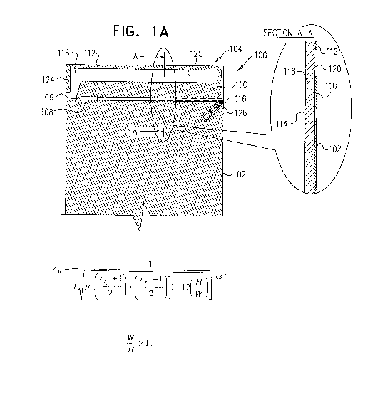
Reference is now made to Figs. 1A and 1B, which are simplified
respective top and underside view illustrations of an antenna, constructed and
operative
in accordance with a preferred embodiment of the present invention.
As seen in Figs. 1A and 1B, there is provided an antenna 100, including a
ground plane 102 and a radiating element 104, an end 106 of which radiating
element
104 is preferably connected to an edge 108 of the ground plane 102.
Preferably,
radiating element 104 is galvanically connected to the edge 108 of the ground
plane
102. Alternatively, radiating element 104 may be non-galvanically connected to
the
edge 108 of the ground plane 102.
As seen most clearly in Fig. 1A, radiating element 104 preferably has a
compact folded configuration including a first portion 110 and a second
portion 112,
which first and second portions 110 and 112 preferably extend generally
parallel to each
other and to the edge 108 of ground plane 102. It is appreciated, however,
that other
configurations of radiating element 104 are also possible and are included
within the
scope of the present invention.
Radiating element 104 is fed by an elongate feed arm 114, which feed
arm 114 is preferably disposed in proximity to but offset from both the first
portion 110
of radiating element 104 and from the edge 108 of the ground plane 102. As
seen most
clearly in section A ¨ A of Fig. 1A, in accordance with a particularly
preferred
embodiment of the present invention, feed arm 114 is disposed in a plane
offset from
the plane in which the radiating element 104 and ground plane 102 are
disposed. Feed
arm 114 receives a radio-frequency (RF) input signal by way of a feed point
116
preferably located thereon. Preferably, feed arm 114 has an open-ended
structure.
Alternatively, feed arm 114 may terminate in other configurations, including a
galvanic
connection to the ground plane 102.
As best seen at section A - A of Fig. 1A, feed arm 114 is very narrow.
The extremely narrow width of feed arm 114 is a particular feature of a
preferred
embodiment of the present invention and confers significant operational
advantages on
antenna 100. The narrow width of feed arm 114 serves, among other features, to
CA 02823547 2013-07-02
WO 2012/093391 PCT/IL2012/000001
distinguish the antenna of the present invention over conventional, seemingly
comparable antennas that typically utilize significantly wider feeding
elements.
Due to its narrow elongate structure, feed arm 114 has a high series
inductance. Furthermore, the close proximity of feed arm 114 to the edge 108
of ground
plane 102 confers a significant shunt capacitance on the ground plane 10/ The
compensatory interaction of these two reactances, namely the series inductance
and
shunt capacitance, leads to improved impedance matching between radiating
element
104 and feed point 116. This improved impedance matching allows radiating
element
104 to operate as a wideband radiating element, capable of radiating
efficiently over a
broad range of frequencies despite its compact folded structure. The mechanism
via
which the elongate narrow feed arm 114 contributes to the wideband operation
of
radiating element 104 will be further detailed henceforth.
Antenna 100 is preferably supported by a non-conductive substrate 118.
Substrate 118 is preferably a printed circuit board (PCB) substrate and may be
formed
of any suitable non-conductive material, including, by way of example, FR-4.
As seen most clearly in sections A ¨ A and B - B of Figs. 1A and 1B
respectively, ground plane 102 and radiating element 104 are preferably
disposed on an
upper surface 120 of substrate 118 and feed arm 114 is preferably disposed on
an
opposite lower surface 122 of substrate 118. However, it is appreciated that
the
reference to upper and lower surfaces 120 and 122 is exemplary only and that
feed arm
114 may alternatively be located on upper surface 120 of substrate 118 and
ground
plane 102 and radiating element 104 located on lower surface 122 of substrate
118. It is
further appreciated that, depending on design requirements, feed arm 114 may
optionally be disposed on the same surface of substrate 118 as that of ground
plane 102
and radiating element 104, provided that feed arm 114 remains offset from both
the
edge 108 of ground plane 102 and radiating element 104.
In operation of antenna 100, feed arm 114 receives an RF input signal by
way of feed point 116. Consequently, near field coupling occurs between feed
arm 114,
the adjacent edge 108 of ground plane 102 and the adjacent first portion 110
of the
radiating element 104. This near field coupling is both capacitive and
inductive in its
nature, its inductive component arising due to the narrow elongate structure
of feed arm
6
= CA 02823547 2013-07-02
WO 2012/093391 PCT/IL2012/000001
114. The near field inductive and capacitive coupling controls the impedance
match of
radiating element 104 to feed point 116.
In effect, feed arm 114, the edge 108 of ground plane 102 and the lower
portion 110 of radiating element 104 function in combination as a loosely
coupled
transmission line terminated in a short circuit by end 106, which loosely
coupled
transmission line feeds the upper portion 112 of the radiating element 104.
The loosely
coupled nature of the transmission line is attributable to the feed arm 114
being
disposed in proximity to but offset from the radiating element 104 and ground
plane
102. The loosely coupled nature of the transmission line is further enhanced
by the gap
between the lower portion 110 of radiating element 104 and the edge 108 of the
ground
plane, which gap is preferably conductor-free, save for the connection of the
lower
portion 110 at end 106 to the edge 108.
The loosely coupled transmission line thus formed acts as a distributed
matching circuit, leading to improved impedance matching over the frequency
band of
radiation of radiating element 104 and hence endowing radiating element 104
with
wideband performance.
It is appreciated that the improved impedance matching between
radiating element 104 and feed point 116 is due in large part to the
compensatory
interaction of the significant series inductive coupling component arising
from the
narrow elongate structure of the feed arm 114 and the shunt capacitive
coupling
component arising from the close proximity of feed arm 114 to the ground plane
edge
108. In the absence of the series inductive coupling component, near field
capacitive
coupling alone would provide a poorer impedance match and hence narrower
bandwidth
of performance of radiating element 104.
Feed arm 114 preferably has a maximum width of 1/100 of a
predetermined wavelength?,, which predetermined wavelength Xp is preferably
defined
by:
A. = ______________________________________________________
-ler +1\ (Cr(e ("
f lli 2 + '2 1+121¨
II -
7
CA 02823547 2013-07-02
WO 2012/093391 PCT/1L2012/000001
wherein f is a lowest operating frequency of radiating element 104, 11 is the
permeability
of substrate 118, sr is the relative bulk permittivity of substrate 118, W is
the width of a
conductive trace disposed above substrate 118, forming a microstrip
transmission line
bounded by air, and H is the thickness of substrate 118. The expression
-0.5
r''24-1)-1-[er' __ [ 1+12 ¨ 11
1 corresponds to the effective dielectric constant
2 L W
for the substrate system. This definition of Xi, assumes that ¨ 1 and is based
upon
equations derived by I. J. Bahl and D. K. Trivedi in "A Designer's Guide to
Microstrip
Line", Microwaves, May 1977, pp. 174-182.
It is appreciated that the conductive trace referenced in the above
equation is simply an entity of computational convenience, used in order to
define the
substrate-specific wavelength corresponding the lowest operating frequency of
radiating
element 104 and hence the preferable maximum width of feed arm 114. It is
understood
that such a conductive trace is not necessarily actually formed in a preferred
embodiment of substrate 118.
Wideband radiating element 104 preferably operates as a low-band
radiating element, preferably capable of radiating in at least one of the LTE
700, LIE
750, GSM 850, GSM 900 and 700-960 MHz frequency bands. Thus, by way of
example, when wideband radiating element 104 operates at a lowest frequency of
700
MHz, the predetermined wavelength Xi, corresponding to 700 MHz and defined
with
respect to a 50 Ohm microstrip transmission line formed of a 1mm thick FR-4
PCB
substrate 118 is approximately 230 mm. The maximum width of feed arm 114
according to this exemplary embodiment is approximately 2.3 mm.
Radiating element 104 preferably has a total physical length
approximately equal to a quarter of its operating wavelength. It is
appreciated that the
first portion 110 of radiating element 104 thus has a dual function, in that
it both
contributes to the near field coupling between the feed arm 114 and the
radiating
element 104, as described above, and constitutes a portion of the total length
of
radiating element 104. A second end 124 of radiating element 104, distal from
its first
end 106 connected to ground plane 102, is preferably bent in a direction
towards edge
8
CA 02823547 2013-07-02
WO 2012/093391 PCT/IL2012/000001
108 of ground plane 102, whereby radiating element 104 is arranged in a
compact
fashion.
Antenna 100 operates optimally when radiating element 104 is located in
close proximity to the edge 108 of ground plane 102, due to the contribution
of the edge
108 of the ground plane 102 to the above-described effective matching circuit.
Particularly preferably, first portion 110 of radiating element 104 is
separated from the
edge 108 of the ground plane 102 by a distance of less than 1/80 of the above-
defined
predetermined wavelength kp. Thus, by way of example, when wideband radiating
element 104 operates at a lowest frequency of 700 MHz, the predetermined
wavelength
corresponding to 700 MHz and defined with respect to a 50 Ohm microstrip
transmission line formed of a lmm thick FR-4 PCB substrate 118 is
approximately 230
mm. The separation of first portion 110 of radiating element 104 from the edge
108 of
the ground plane, according to this exemplary embodiment, is less than
approximately
2.8 mm.
The close proximity of radiating element 104 to the ground plane 102 is a
highly unusual feature of antenna 100 in comparison to conventional antennas
that
typically require the radiating element to be at a greater distance from the
ground plane,
in order to prevent degradation of the operating bandwidth and radiating
efficiency of
the antenna. The location of the radiating element 104 in such close proximity
to the
ground plane 102 in antenna 100 allows antenna 100 to be advantageously
compact.
The extent of the coupling between feed arm 114, the edge 108 of the
ground plane 102 and the first portion 110 of the radiating element 104 is
influenced by
various geometric parameters of antenna 100, including the length and width of
the feed
arm 114, the configuration of the first and second portions 110 and 112 of
radiating
element 104 and the respective separations of first portion 110 and second end
124 of
radiating element 104 from the edge 108 of the ground plane 102.
Feed arm 114 and radiating element 104 may be embodied as three-
dimensional conductive traces bonded to substrate 118, or as two-dimensional
conductive structures printed on the surfaces 120 and 122 of substrate 118. A
discrete
passive component matching circuit, such as a matching circuit 126, may
optionally be
included within the RF feedline driving antenna 100, prior to the feed point
116.
9
CA 02823547 2013-07-02
WO 2012/093391 PCT/IL2012/000001
Reference is now made to Fig. 2, which is a simplified graph showing the
return loss of an antenna of the type illustrated in Figs. 1A and 1B.
First local minima A of the graph generally corresponds to the frequency
response of antenna 100 provided by radiating element 104. As is evident from
consideration of the width of region A, the response of antenna 100 is
wideband and
spans, by way of example, a range of 700 ¨ 960 MHz with a return loss of
better than ¨5
dB. As described above with reference to Figs. 1A and 1B, the wideband low-
frequency
response of antenna 100 is due to the improved impedance match of radiating
element
104 to feed point 116, as a result of the narrow elongate structure of feed
arm 114.
As is evident from consideration of region B of the graph, antenna 100
does not exhibit a significant high-band response. This is because feed arm
114 does not
have a significant high-frequency resonant response associated with it, due to
its narrow
structure and very close proximity to the ground plane 102. The poor radiating
performance of feed arm 114 is an advantageous feature of antenna 100, since
it allows
the addition of a separate high-band radiating element, capable of operating
with
negligible dependence on low-band radiating element 104, as will be detailed
below
with reference to Figs. 3A ¨ 3C.
Reference is now made to Figs. 3A, 3B and 3C which are simplified
respective top, underside and side view illustrations of an antenna,
constructed and
operative in accordance with another preferred embodiment of the present
invention.
As seen in Figs. 3A ¨ 3C, there is provided an antenna 300, including a
ground plane 302 and a first wideband radiating element 304, connected at one
end 306
thereof with an edge 308 of the ground plane 302 and including a first portion
310 and a
second portion 312. First wideband radiating element 304 is fed by a narrow
feed arm
314 preferably having a feed point 316 located thereon. As seen most clearly
in sections
A ¨A and B- B of Figs. 3A and 3B respectively, feed arm 314 is preferably
disposed in
proximity to but offset from ground plane 302 and first portion 310 of
radiating element
304. Particularly preferably, feed arm 314 is disposed in a plane offset from
the plane in
which radiating element 304 and ground plane 302 are disposed.
Antenna 300 is preferably supported by a non-conductive substrate 318
having respective upper and lower surfaces 320 and 322, on which upper surface
320
= CA 02823547 2013-07-02
WO 2012/093391 PCT/1L2012/000001
ground plane 302 and radiating element 304 are preferably located and on which
lower
surface 322 feed arm 314 is preferably located.
Feed arm 314 preferably has a maximum width of 1/100 of a
predetermined wavelength 4, which predetermined wavelength 4 is preferably
defined
by:
1
A=
r Er +1\ er l
f i`2 ________________________________ + ____ 1+121¨
2
wherein f is a lowest operating frequency of radiating element 304,1A is the
permeability
of substrate 318, Cr 15 the relative bulk permittivity of substrate 318, W is
the width of a
conductive trace disposed above the substrate 318, forming a microstrip
transmission
line bounded by air, and H is the thickness of substrate 318. The expression
(E, +1) ( 2 er ¨1 u. -0 5
________________ ' II
1+12( corresponds to the effective dielectric constant
2
for the substrate system. This definition of 4 assumes that ¨ 1 and is based
upon
equations derived by I. J. Bahl and D. K. Trivedi in "A Designer's Guide to
Microstrip
Line", Microwaves, May 1977, pp. 174-182.
First portion 310 of radiating element 304 is preferably separated from
the edge 308 of the ground plane 302 by a distance of less than 1/80 the above-
defined
predetermined wavelength Xv.
It is appreciated that antenna 300 may resemble antenna 100 in every
relevant respect, with the exception of the inclusion of a second radiating
element 330
in antenna 300. Second radiating element 330 shares feed point 316 with feed
arm 314
and is preferably galvanically connected to feed point 316, as seen most
clearly in Fig.
3B.
As seen most clearly in Fig. 3C, second radiating element 330 is
preferably disposed in a plane offset from the plane defined by substrate 318.
In
accordance with a particularly preferred embodiment of the present invention,
second
radiating element 330 is disposed in a plane offset from the plane defined by
substrate
318 by a distance of 4 mm. In accordance with another particularly preferred=
11
CA 02823547 2013-07-02
WO 2012/093391 PCT/1L2012/000001
embodiment of the present invention, second radiating element 330 is disposed
in a
plane offset from the plane defined by substrate 318 by a distance of 7 mm.
In operation of antenna 300, first radiating element 304 preferably
operates as a wideband low-frequency radiating element, generally in
accordance with
the mechanism described above in reference to low-frequency wideband radiating
element 104 of antenna 100. Additionally, second radiating element 330
preferably
operates as a high-frequency radiating element fed by feed point 316. Antenna
300 thus
operates as a multiband antenna, capable of radiating in low- and high-
frequency bands,
respectively provided by first and second radiating elements 304 and 330.
It is a particular feature of a preferred embodiment of the present
invention that respective first and second radiating elements 304 and 330
operate with
an exceptionally low degree of mutual interdependence, despite being fed by
way of a
common feed point 316. The low and high operating frequencies of antenna 300
thus
may be adjusted freely, due to the almost complete absence of the strong low-
band and
high-band tuning interdependencies exhibited by conventional multi-band
antennas.
As described above with reference to Fig. 2, the comparatively
independent operation of the low- and high-frequency radiating elements 304
and 330
of antenna 300 is attributable to the narrow elongate structure of feed arm
314 and its
location in close proximity to the ground plane 302, which features prevent
feed arm
314 from acting as a high-band radiating element in its own right and
therefore from
interfering with the operation of high-band radiating element 330.
Second high-band radiating element 330 may have an inverted L-shaped
configuration, as seen most clearly in Figs. 3A and 3B. It is appreciated,
however, that
the illustrated configuration of second radiating element 330 is exemplary
only and that
other compact configurations are also possible.
Other features and advantages of antenna 300, including its wideband
response due to the improved impedance matching provided by elongate narrow
feed
arm 314, are generally as described above in reference to antenna 100.
Reference is now made to Fig. 4, which is a simplified graph showing the
return loss of an antenna of the type illustrated in Figs. 3A ¨ 3C.
First local minima A of the graph generally corresponds to the wideband
low-frequency band of radiation provided by first radiating element 304 and
second
12
CA 02823547 2013-07-02
WO 2012/093391 PCT/1L2012/000001
local minima B generally corresponds to the high-frequency band of radiation
preferably provided by second radiating element 330.
As is evident from comparison of region A of Fig. 4 to region A of Fig.
2, which regions respectively correspond to the frequency responses of low-
band
radiating element 104 in antenna 100 and low-band radiating element 304 in
antenna
300, the addition of high-band radiating element 330 in antenna 300 does not
detract
from the wideband response of the low-band radiating element.
As shown in Fig. 4, by way of example, the operating frequencies of
second radiating element 330 may be centered around 1800 MHz. However, it is
appreciated that the operating frequencies of second radiating element 330 may
be
adjusted by way of modifications to various geometric parameters of radiating
element
330, including, but not limited to, its total length and separation from the
ground plane
302.
It will be appreciated by persons skilled in the art that the present
invention is not limited by what has been particularly claimed hereinbelow.
Rather, the
scope of the invention includes various combinations and subcombinations of
the
features described hereinabove as well as modifications and variations thereof
as would
occur to persons skilled in the art upon reading the forgoing description with
reference
to the drawings and which are not in the prior art. In particular, it will be
appreciated
that although embodiments including only single ones of the antennas of the
present
invention have been described herein, the inclusion of multiple ones of the
antennas of
the present invention on a single antenna substrate is also possible.
13