Note : Les descriptions sont présentées dans la langue officielle dans laquelle elles ont été soumises.
CA 02823706 2013-07-03
WO 2012/099598
PCT/US2011/022012
1
Z-DIRECTED CAPACITOR COMPONENTS FOR PRINTED CIRCUIT BOARDS
CROSS REFERENCES TO RELATED APPLICATIONS
[0001] This patent application is related to United States Patent
Applications Serial
No. 12,508,131 (Attorney Docket No. 2008-0295.01) entitled "Z-directed
Components for
Printed Circuits Boards"; Serial No. 12,508,145 (Attorney Docket No. 2009-
0117.00) entitled
"Z-directed Pass-Through Components For Printed Circuits Boards"; Serial No.
12,508,188
(Attorney Docket No. 2009-0119.00) entitled "Z-directed Delay Line Components
For
Printed Circuits Boards"; Serial No. 12,508,199 (Attorney Docket No. 2009-
0120.00) entitled
"Z-directed Filter Components For Printed Circuits Boards"; Serial No.
12,508,204 (Attorney
Docket No. 2009-0121.00) entitled "Z-directed Ferrite Bead Components For
Printed Circuits
Boards"; Serial No. 12,508,215 (Attorney Docket No. 2009-0122.00) entitled "Z-
directed
Switch Components For Printed Circuits Boards"; Serial No. 12,508,236
(Attorney Docket
No. 2009-0123.00) entitled "Z-directed Connector Components For Printed
Circuits Boards";
Serial No. 12,508,248 (Attorney Docket No. 2009-0124.00) entitled "Z-directed
Variable
Value Components For Printed Circuits Boards"; each filed July 23, 2009 and
all assigned to
the assignee of the present application.
STATEMENT REGARDING FEDERALLY SPONSORED RESEARCH OR
DEVELOPMENT
[0002] None.
REFERENCE TO SEQUENTIAL LISTING, ETC.
[0003] None.
BACKGROUND
1. Field of the Invention
[0004] The present invention relates electronic components, and more
particularly to
those for insertion into a printed circuit board and methods of assembly.
2. Description of the Related Art
[0005] Printed Circuit Board ("PCB") manufacturing primarily uses two
types of
components. The first type is pin through-hole parts that use metallic leads
that are soldered
into a plated through-hole in the PCB. The second type of component is a
surface mount part
that sits on the surface of a PCB and it attached by soldering to pads on the
surface. As
CA 02823706 2013-07-03
WO 2012/099598
PCT/US2011/022012
2
densities of components have increased and higher frequencies of operation are
used, some
circuits' designs have become very difficult to achieve. The presented
invention improves
the component densities and frequencies of operation.
[0006] Currently resistors can be embedded between layers of a PCB by
applying a
resistive material between two copper traces after the etching step in the
manufacturing
process. A typical 4 layer PCB is made up of two assemblies that are each two
layer PCBs.
These are glued together with a material to become the completed assembly. The
resistive
area can be applied to any layer making it possible to have the resistive
elements on the
interior layers. However this approach is more time consuming and makes
changes difficult
to to implement. The present invention removes these difficulties by
allowing for insertion of
the part to occur after the multilayered PCB is assembled.
SUMMARY OF THE INVENTION
[0007] A Z-directed capacitive component for mounting in a PCB having
a mounting
hole having a depth D therein , comprises an insulative body having a top
surface, a bottom
surface and side surface, a length L, and a cross-sectional shape that is
insertable into the
mounting hole in the PCB; a first and a second electrically conductive channel
on the side
surface with the first channel extending from one of the top and bottom
surfaces and the
second channel extending from the other of the top and bottom surfaces; a
first semi-
cylindrical metallic sheet positioned within the body, extending along the
length of the body
and electrically connected to the first channel, the first sheet extending
toward the second
channel; and a second semi-cylindrical metallic sheet positioned within the
body concentric
with the first metallic sheet and positioned inside of and substantially
uniformly spaced apart
from the first metallic sheet, the second metallic sheet extending along the
length of the body
and toward the first channel wherein a portion of the first and second sheets
overlap one
another with the second sheet electrically connected to the second channel
wherein the first
and second sheets forming a capacitor. The Z-directed component further
comprising a semi-
cylindrical sheet of dielectric material positioned between the first and
second metallic
sheets.
[0008] In another form a Z-directed component for mounting in a PCB
having a
mounting hole having a depth D therein , comprises a body comprising a top
surface, a
bottom surface, side surface, a cross-sectional shape that is insertable into
the mounting hole
in the PCB, a top portion, a bottom portion. Also provided are a plurality of
support
CA 02823706 2013-07-03
WO 2012/099598
PCT/US2011/022012
3
members intermediate the top and bottom portions of the body wherein the top
portion and
bottom portion of the body and each support member has a center opening and a
pair of
opposed openings on a edge thereof with the opposed openings of the top and
bottom
portions and the plurality of support members forming a pair of opposed
channels on the side
surface of the body, each support member comprises an annular plate mounted on
a surface
of the support member, the annular plate having a center opening having a
dimension that is
larger than the center opening in the support member and an outer dimension
that is less than
the outer dimension of the support member on which it is mounted, the annular
plate connects
with one opening in the pair of opposed openings in the support member. A
conductor
to extends the length of the body between the top and bottom surfaces of
the body and passes
through the center openings of the plurality of support plates and the top and
bottom portions
of the body; and a pair of conductive traces, one on each of the top and
bottom surfaces of the
body electrically connected to an end of the conductor adjacent thereto and
extending
therefrom to an edge of the body, the conductive traces and conductor creating
a signal path
through the Z-directed component, wherein the plurality of support members are
arranged
such that the annular plate of one support member electrically contacts one of
the opposed
channels while the annular plate on the next support member electrically
contacts the other
one of the opposed channels.
[0009] In a further embodiment a plurality of dielectric disks is
interleaved with the
support members, each dielectric disk having center opening therethrough for
receiving the
conductor therein and a pair of opposed openings on a edge thereof with the
opposed
openings of the top and bottom portions, the plurality of dielectric disks and
the plurality of
support members forming the pair of opposed channels on the side surface of
the body.
[0010] In another embodiment, an electrical connector is provided
between the
conductor and at least one of the annular plates. Here the conductive traces
on the top and
bottom surfaces of the body do not extend to the edge of the body.
[0011] In another form a Z-directed component for mounting in a PCB
having a
mounting hole having a depth D therein , comprises a body comprising a top
surface, a
bottom surface, side surface, a cross-sectional shape that is insertable into
the mounting hole
in the PCB, a top portion, a bottom portion; and a plurality of support
members intermediate
the top and bottom portions of the body wherein the top portion and bottom
portion of the
body and each support member has a center opening and a pair of opposed
openings on a
edge thereof with the opposed openings of the top and bottom portions and the
plurality of
CA 02823706 2013-07-03
WO 2012/099598
PCT/US2011/022012
4
support members forming a pair of opposed channels on the side surface of the
body. Each
support member comprises an annular plate mounted on a surface of the support
member, the
annular plate having a center opening having a dimension that is larger than
the center
opening in the support member and an outer dimension that is less than the
outer dimension
of the support member on which it is mounted. A first conductor extends the
length of the
body between the top and bottom surfaces of the body and passes through the
center openings
of the plurality of support plates and the top and bottom portions of the
body; and a pair of
conductive traces, one on each of the top and bottom surfaces of the body
electrically
connected to an end of the first conductor adjacent thereto and extending
therefrom to an
to edge of the body, the conductive traces and first conductor creating a
signal path through the
Z-directed component. An at least one second conductor disposed within the
body having
one end electrically connected to one of the annular plates and the other end
extending to the
side surface of the body. A plurality of dielectric disks interleaved with the
support members
may also be provided, each dielectric disk having a center opening
therethrough for receiving
the first conductor therein and a pair of opposed openings on a edge thereof
with the opposed
openings of the top and bottom portions, the plurality of dielectric disks and
the plurality of
support members forming the pair of opposed channels on the side surface of
the body.
[0012] In another form, the at least one second conductor further
comprises a
plurality of conductors corresponding to the plurality of annular rings, each
of the plurality of
conductors having one end electrically connected to a corresponding one of the
plurality of
annular rings and the other end extending to the side surface of the body and
can be aligned
along the length of the body.
BRIEF DESCRIPTION OF THE DRAWINGS
[0013] The above-mentioned and other features and advantages of the
various
embodiments of the invention, and the manner of attaining them, will become
more apparent
will be better understood by reference to the accompanying drawings, wherein:
Figure 1 is an illustration of one embodiment of a Z-directed component;
Figure 2 is an illustrates the internal arrangement of elements comprising one
embodiment of the Z-directed component of Figure 1;
Figures 3A ¨ 3F illustrate various shapes for the body of a Z-directed
component;
CA 02823706 2013-07-03
WO 2012/099598
PCT/US2011/022012
Figures 4A ¨ 4C illustrate various channel configurations for a Z-directed
component;
Figures 5A ¨ 5H illustrate various channel and conductor configurations for
the body of a Z-directed component;
5 Figures 6A ¨ 6D illustrate various orienting locating or connection
features of
a Z-directed component;
Figures 7A and 7B illustrate a Z-directed component having 0-rings for
connecting to internal layers of a PCB and having a body having regions
comprised of similar
and or dissimilar materials;
Figure 8 illustrates various elements or electronic components such as a
resistor, diode, capacitor that may be provided within the body of a Z-
directed component in
series with a conductor;
Figure 9 illustrates a Z-directed component having a 3-terminal transistor
connected to two conductors;
Figure 10 illustrates an alternate embodiment of a Z-directed component
having a 3-terminal transistor connected to a conductor and a plated channel;
Figure 11 illustrates a cross-sectional view of the embodiment of a Z-directed
component flush mounted within a PCB shown in Figure 12;
Figure 12 illustrates a top view of the PCB and the Z-directed component of
Figure 11 showing the conductive traces and connections to the Z-directed
component;
Figure 13 illustrates ground loops for the Z-directed component of Figures 11
and 12 with the Z-directed component further comprising with a decoupling
capacitor within
the body of the Z-directed component;
Figure 14 is an illustration of a Z-directed component for transferring a
signal
trace from one internal layer of a PCB to another internal layer of that PCB;
Figure 15 is an illustration of one embodiment of a Z-directed capacitor
comprising semi-cylindrical sheets;
Figure 16 is an exploded view illustration of another embodiment of a Z-
directed capacitor comprising stacked discs;
CA 02823706 2013-09-09
6
Figures 17A ¨ 17C illustrate alternate embodiments of a Z-directed delay line
with transparent surfaces to display connections;
Figure 18 illustrates a programmable Z-directed delay line circuit having
multiple Z-directed delay lines with transparent surfaces to display
connections;
Figures 19A ¨ 19C illustrate sectional views of a single conductor
differential
Z-directed ferrite bead, a 2 conductor differential mode Z-directed ferrite
bead, and a 2
conductor common mode Z-directed ferrite bead;
Figures 20A and 20B illustrate a Z-directed switch component that can be
rotated to connect predetermined circuit paths in a PCB;
to Figure 20B is a sectional illustration of the PCB taken along line
20B-20B of
Figure 20A with the Z-directed switch component removed to show internal
connection
points of the PCB;
Figure 20C is an illustration of the Z-directed switch component of Figure
20A having an internal electronic component;
Figure 20D is a top view of the Z-directed switch component of Figure 20C
showing alternate configurations of the channel shapes and conductive member
and radial
projections;
Figures 21A ¨ 21D illustrate a Z-directed component utilized for making
internal connections between traces on different internal layers or between
traces on a given
internal layer of a PCB along with an additional feature of a testing path for
checking the
connections;
Figures 22A and 22B illustrate the use of a plateable side strip and partial
insertion of Z-directed components to alter value or function of the Z-
directed component;
Figure 23 is an illustration of a system for inserting Z-directed components
into a PCB;
Figure 24 is an illustration of a Z-directed component having a glue strip and
a
glue dot for mounting of the Z-directed component in a PCB; and
Figure 25 is an illustration of a Z-directed component showing copper seed
material and resist material used when plating a Z-directed component.
DETAILED DESCRIPTION
CA 02823706 2013-07-03
WO 2012/099598
PCT/US2011/022012
7
[0014] The present invention will now be described more fully
hereinafter with
reference to the accompanying drawing figures, in which some, but not all
embodiments of
the invention are shown. It is to be understood that the invention is not
limited in its
application to the details of construction and the arrangement of components
set forth in the
following description or illustrated in the drawings. The invention may be
embodied in many
different forms and should not be construed as limited to the embodiments set
forth herein;
rather, these embodiments are provided so that this disclosure will satisfy
applicable legal
requirements.
[0015] The phraseology and terminology used herein is for the purpose
of description
to and should not be regarded as limiting. The use of "including,"
"comprising," or "having"
and variations thereof herein is meant to encompass the items listed
thereafter and
equivalents thereof as well as additional items. Unless limited otherwise, the
terms
"connected," "coupled," and "mounted," and variations thereof herein are used
broadly and
encompass direct and indirect connections, couplings, and mountings. In
addition, the terms
"connected" and "coupled" and variations thereof are not restricted to
physical or mechanical
connections or couplings.
[0016] As described in subsequent paragraphs, the specific mechanical
configurations
illustrated in the drawings are intended to exemplify embodiments of the
invention and that
other alternative mechanical configurations are possible.
[0017] This specification describes a family of components that are
intended to be
embedded or inserted into a PCB. These components are termed Z-directed
components and
have been modeled and basic prototypes of many of the components described
herein, but
lacking the surface channels, were made to establish proof of concept. Not all
embodiments
described herein have been constructed. An overview of how Z-directed
components are
intended to be formed is presented initially followed by configurations for Z-
directed
component designs including but not limited to capacitors, delay lines,
transistors, switches,
and connectors. This is followed by techniques believed to be useful for
assembling PCBs
with Z-directed components. Z-directed components occupy less space on the
surface of a
PCB and for high frequency circuits (e.g. clock rates greater than 1000MHz)
allow for higher
frequency of operation.
Overview
CA 02823706 2013-07-03
WO 2012/099598
PCT/US2011/022012
8
[0018] As used here in an X-Y-Z frame of reference is used. The X and
Y axes
describe the plane of a printed circuit board. The Z-axis describes a
direction perpendicular
to the plane of the circuit board. The top surface of the PCB has a zero Z-
value. A
component with a negative Z-direction value indicates that the component is
inserted into the
top surface of the PCB. Such a component may be above (extend past), flush
with, or
recessed below either the top surface and/or the bottom surface of the PCB. A
component
having both a positive and negative Z-direction value indicates that the
component is partially
inserted into the surface of the PCB. Z-directed components are intended to be
inserted into a
hole or recess in a printed circuit board. Depending on its shape and length
more than one Z-
directed component may be inserted into a single mounting hole in the PCB,
such as being
stacked together or positioned side by side. The hole may be a through hole (a
hole from the
top surface through to the bottom surface) or a well (an opening or recess
through either the
top or bottom surface into an interior portion or internal layer of the PCB.
[0019] As described herein the Z-directed components are illustrated
as being inserted
into the top surface of the PCB. For a PCB having conductive traces on both
external layers,
one external layer is termed the top surface and the other the bottom surface.
Also where
only one external layer has conductive traces, that external surface is
referred to as the top
surface. The Z-directed component is referred to as having a top surface, a
bottom surface
and a side surface. The references to top and bottom surfaces of the Z-
directed component
conform to the convention used to refer to the top and bottom surfaces of the
PCB. The side
surface of a Z-directed component is in the Z-direction and would be adjacent
to the wall of
the mounting hole in the PCB which is also in the Z-direction. This use of
top, bottom and
side should not be taken as limiting how a Z-directed component may be mounted
into a
PCB. Although the components are described herein as being mounted in a Z-
direction, this
does not mean that such components are limited to being inserted into a PCB
only along the
Z-axis. Z-directed components may be mounted normal to the plane of the PCB
from the top
or bottom surfaces or both surfaces, mounted at an angle thereto or, depending
on the
thickness of the PCB and the dimensions of the Z-directed component and even
inserted into
the edge of the PCB between to the top and bottom surfaces of the PCB.
[0020] The Z-directed components may be made from various combinations of
materials commonly used in electronic components. The signal connection paths
will be
made from conductors which are materials that have high conductivity.
Conducting materials
include, but are not limited to, copper, gold, aluminum, silver, tin, lead and
many others. Z-
CA 02823706 2013-07-03
WO 2012/099598
PCT/US2011/022012
9
directed components will have areas that need to be insulated from other areas
by using
materials that have low conductivity like plastic, glass, FR4 (epoxy &
fiberglass), air, mica,
ceramic and others. A Z-directed component that is constructed as a resistor
requires
materials that have properties that are between a conductor and insulator
which have a finite
amount of resistivity which is the reciprocal of conductivity. Materials like
carbon, doped
semiconductor, nichrome, tin-oxide and others are used for their resistive
properties.
Capacitors are typically made of two conducting plates separated by an
insulating material
that has a high permittivity (dielectric constant). Permittivity is a
parameter that shows the
ability to store electric fields in the materials like ceramic, mica, tantalum
and others.
to Inductors are typically made of coils of wires or conductors wrapped
around a material with
high permeability. Permeability is a parameter that shows the ability to store
magnetic fields
in the material which are iron and alloys like nickel-zinc, manganese-zinc,
nickel-iron and
others. Transistors and FET are electronic devices that are made from
semiconductors that
behave in a nonlinear fashion and are made from silicon, germanium, gallium
arsenide and
others. Throughout the application there are references that discuss different
materials,
properties of materials or terminology interchangeably as currently used in
the art of material
science and electrical component design. Because of the flexibility in how a Z-
directed
component is constructed and the number of materials that may be used, it is
also
contemplated that Z-directed components may be constructed of materials that
have not been
discovered or created to date. The body of a Z-directed component will in
general be
comprised of a non-conductive material unless otherwise called out in the
description for a
particular design of a Z-directed component such as a capacitor.
[0021] The PCB which uses a Z-directed component may be constructed to
have a
single conductive layer or multiple conductive layers as is known. The PCB may
have
conductive traces on the top surface only, on the bottom surface only, on both
the top and
bottom surfaces. In addition one or more intermediate internal conductive
trace layers may
also be present in the PCB.
[0022] Connections between a Z-directed component and the traces in or
on a PCB
may be accomplished by soldering techniques, screening techniques, extruding
techniques or
plating techniques as are known in the art. Depending upon application, solder
pastes and
component adhesives may be used. In some configurations, compressive
conductive
members may be used to interconnect a Z-directed component to conductive
traces found on
the PCB.
CA 02823706 2013-07-03
WO 2012/099598
PCT/US2011/022012
Z-directed Components
[0023] The most general form a Z-directed component comprises a body
having a top
surface, a bottom surface and a side surface, a cross-sectional shape that is
insertable into a
mounting hole of a given depth D within a PCB with a portion of the body
comprising an
5 insulator. All of the embodiments described herein for Z-directed
components are based on
this general form.
[0024] Figures 1 and 2 show an embodiment of a Z-directed component.
There Z-
directed component 10 comprises a generally cylindrical body 12 having a top
surface 12t, a
bottom surface 12b, a side surface 12s, and a length L generally corresponding
to the depth D
to of the mounting hole. The length L can be less than, equal to or greater
than the depth D. In
the former two cases, Z-directed component 10 would in one case be below at
least one of the
top and bottom surfaces of the PCB and in the other it would be flush with the
two surfaces
of the PCB. Where length L is greater than depth D, Z-directed component 10
would not be
flush mounted. However with this non-flush mount, Z-directed component 10
would be
capable of being used to interconnect to another component or another PCB that
is positioned
nearby. The mounting hole is typically a through-hole extending between the
top and bottom
surfaces of the PCB but it may also be a blind hole. When recessed below the
surface of the
PCB additional resist areas may be required in the hole of the PCB to keep
from plating the
entire circumferential area around the hole.
[0025] Z-directed component 10 in one form may have at least one conductor
14
extending through the length of body 12. At the top and bottom ends 14t and
14b of
conductor 14 top and bottom conductive traces 16t, 16b are provided on the top
and bottom
end surfaces 12t, 12b of body 12 and extend from respective ends of the
conductor 14 to the
edge of Z-directed component 10. In this embodiment body 12 comprises a non-
conductive
material. Depending on its function, body 12 of Z-directed component 10 may be
made of
variety of materials having different properties. These properties include
being conductive,
resistive, magnetic, dielectric, or semiconductive or various combinations of
properties as
described herein. Examples of materials that have the properties are copper,
carbon, iron,
ceramic or silicon, respectively. Body 12 of Z-directed component 10 may also
comprise a
number of different networks needed to operate a circuit that will be
discussed later.
[0026] One or more longitudinally extending channels or wells may be
provided on
the side surface of body of Z-directed component 10. The channel may extend
from one of
CA 02823706 2013-07-03
WO 2012/099598
PCT/US2011/022012
11
the top surface and the bottom surface of body 12 toward the opposite surface.
As illustrated
two concave wells or channels 18 and 20 are provided in the outer surface of Z-
directed
component 10 extending the length of body 12. When plated or soldered, these
channels
allow electrical connections to be made to Z-directed component 10, through
the PCB, as
well as to internal conductive layers within the PCB. The length of the
channels 18 or 20
may extend less than the entire length of body 12.
[0027] Figure 2 shows the same component as in Figure 1 but with all
the surfaces
transparent. The conductor 14 is shown as a cylinder extending through the
center of Z-
directed component 10. Other shapes may also be used for conductor 14. Traces
16t and 16b
to can be seen extending from conductor ends 14t and 14b, respectively to
the edge of body 12
is a conductor that connects the top trace 16t to the bottom trace 16b. While
traces 16t and
16b are shown as being in alignment with one another (zero degrees apart) this
is not a
requirement and they may be positioned as needed for a particular design. For
example
traces 16t and 16b may be 180 degrees apart or 90 degrees apart and any all
increments
therein.
[0028] Body shape may be any shape that can fit into a mounting hole
in a PCB.
Figures 3A ¨ 3F illustrate possible body shapes for a Z-directed component.
Figure 3A
shows a triangular cross-sectional body 40; Figure 3B a rectangular cross
sectional body 42;
Figure 3C a frusto-conical body 44; Figure 3D an ovate cross sectional
cylindrical body 46;
and Figure 3E a cylindrical body 48. Figure 3F is a stepped cylindrical body
50 where one
portion 52 has a larger diameter than another portion 54. With this
arrangement the Z-
directed component may be mounted on the surface of the PCB while having a
section being
inserted into the mounting hole provided in the PCB. The edges of Z-directed
component
may be beveled to help with aligning the Z-directed component for insertion
into a through-
hole in a PCB. Other shapes and combinations of those illustrated may also be
used for a Z-
directed component.
[0029] For a Z-directed component, the channels for plating can be of
various cross-
sectional shapes and lengths. The only requirement is that plating or solder
material make the
proper connections to the Z-directed component and corresponding conductive
traces in or on
the PCB. Channels 18 or 20 may have, for example, V-, C- or U-shaped cross
sections, semi-
circular or elliptical cross sections. Where more than one channel is
provided, each channel
may have a different cross-sectional shape. Figures 4A ¨ 4C illustrate three
channel shapes.
CA 02823706 2013-07-03
WO 2012/099598
PCT/US2011/022012
12
In Figure 4A V- shaped channels 60 are shown. In Figure 4B, U- or C-shaped
channels 62
are shown. In Figure 4C, wavy or irregular cross-sectional channel shapes 65
are shown.
[0030] The numbers of layers in a PCB varies from being single sided
to being over
22 layers and may have different overall thickness that range from less than
0.051 inch to
over 0.093 inch or more. Where a flush mount is desired the length of the Z-
directed
component will depend on of the thickness of the PCB into which is intended to
be inserted.
The Z-directed component's length may also vary depending of the intended
function and
tolerance of a process. The preferred lengths will be where the Z-directed
component is
either flush the surfaces or extends slightly beyond the surface of the PCB.
This would keep
to the plating solution from plating completely around the interior of the
PCB hole that may
cause a short in some cases. It is possible to add a resist material around
the interior of a
PCB hole to only allow plating in the desired areas. However, there are some
cases where it
is desired to completely plate around the interior of a PCB hole above and
below the Z-
directed component. For example if the top layer of the PCB was a Vcc plane
and the bottom
layer is a GND plane then a decoupling capacitor would have lower impedance if
the
connection used a greater volume of copper to make the connection.
[0031] There are number of features that can be added to a Z-directed
component to
create different mechanical and electrical characteristics. The number of
channels or
conductors can be varied from zero to any number that can maintain enough
strength to take
the stresses of insertion, plating, manufacturing processes and operation of
the PCB in its
intended environment. The outer surface of a Z-directed component may have a
coating that
glues it in place. Flanges or radial projections may also be used to prevent
over or under
insertion of a Z-directed component into the mounting hole, particular where
the mounting
hole is a through-hole. A surface coating material may also be used to promote
or impede
migration of the plating or solder material.
[0032] A Z-directed component may take on several roles depending on
the number
of ports or terminals needed to make connections to the PCB. Some
possibilities are shown
in Figures 5A ¨ H. Figure 5A is a Z-directed component configured as 0-port
device 70A
used as a plug so that if a filter or a component is optional then the plug
stops the hole from
being plated. After the PCB has been manufactured, the 0-port device 70A may
be removed
and another Z-directed component may be inserted, plated and connected to the
circuit.
Figures 5B ¨ 5H illustrate various configurations useful for multi-terminal
devices such as
resistor, diode, transistor, clock circuit. Figure 5B shows a 1-port or single
signal Z-directed
CA 02823706 2013-07-03
WO 2012/099598
PCT/US2011/022012
13
component 70B having a conductor 71 connected to top and bottom conductive
traces 72t,
72b. Figure 5C shows a 1-port 1-channel Z-directed component 70C where one
plated well
or channel 73 is provided in addition to conductor 71 and top and bottom
conductive traces
72t and 72b. Figure 5D shows a Z-directed component 70D having two wells 73
and 75 in
addition to conductor 71 and top and bottom traces 72t, 72b. The Z-directed
component 70E
of Figure 5E has three wells 73, 75 and 76 in addition to conductor 71 and top
and bottom
traces 72t, 72b. Figure 5F shows Z-directed component 70F having two
conductors 71 and
77 each with their respective top and bottom traces 72t, 72b and 78t, 78b and
no channels or
wells. Z-directed component 70F is a two signal device to be primarily used
for differential
to signaling. Figure 5G shows a Z-directed component 70G having one well 73
and two
conductors 71 and 77 each with their respective top and bottom traces 72t, 72b
and 78t, 78b.
Figure 5H shows Z-directed component 70H having one conductor 71 with top and
bottom
traces 72t, 72b and a blind well or partial well 78 extending from the top
surface along a
portion of the side surface that will allow the plating material or solder to
stop at a given
depth. For one skilled in the art, the number of wells and signals is only
limited by the space,
required well size and conductor sizes.
[0033] In most cases Z-directed components will need to be orientated
correctly when
inserted into a PCB. Accordingly, locating or orienting features and
connections features
may be provided. Figures 6A ¨ 6C illustrate examples of such locating features
while Figure
6D illustrate a connection feature. In Figure 6A, Z-directed component 80A has
a V-notch
81 on an end surface extending radially outward. In Figure 6B, Z-directed
component 80B
has a recess 83 on an end surface of Z-directed component 80B having an
orienting surface
84. Figure 6C shows Z-directed component 80C having an axial projection, peg
85,
extending axially outward from an end surface and having an orienting surface
86. An ink
mark or other visual or magnetic indicator on an end surface or on the side of
a Z-directed
component may also be used to orient a Z-directed component such as when using
a camera.
[0034] As shown in Figure 6D, Z-directed component 80D may be fitted
with a
connection feature such as a conductive pad, a spring loaded style pogo-pin or
even a simple
spring 88 that may be used to add an additional electrical connection (such as
frame ground)
point to a printed circuit board. Spring 88 is illustrated as being connected
to conductor 89 of
Z-directed component 80D.
[0035] Figures 7A and 7B illustrate another configuration for a Z-
directed component
utilizing 0-rings for use in a PCB having a top and bottom conductive layer
and at least one
CA 02823706 2013-07-03
WO 2012/099598
PCT/US2011/022012
14
internal conductive layer. Z-directed component 150 is shown having on its top
surface 150t,
a locating feature 152 and conductive top trace 154t extending between
conductor 156 and
the edge of body 150d on its top surface 150t. (A conductive bottom trace not
shown is
provided on the bottom surface). Conductor 156 extends through a portion of
the body 150d
as previously described. Located on the side surface 150s of body 150d is a
least one semi-
circular channel or grove. As shown a pair of axially spaced apart
circumferential channels
158a, 158b are provided having 0-rings 160a, 160b, respectively disposed
within channels
158a, 158b. A portion of the 0-rings extend out beyond the side surface 150s
of the body
150d. 0-rings 160a, 160b would be positioned adjacent one or more of the
internal layers of
to the PCB to make electrical contract to one or more traces provided at
that point in the
mounting hole for the Z-directed component. Depending on the design an 0-ring
would not
have to be provided adjacent every internal layer.
[0036] 0-rings 160a, 160b may be conductive or non-conductive
depending on the
design of the circuit in which they are used. 0-rings 160a, 160b preferably
would be
compressive helping to secure Z-directed component 150 within the mounting
hole. The
region 162 of body 150d intermediate 0-rings 160a, 160b may be comprised of
different
material than the regions 164 and 166 of the body 150d outside of the 0-rings.
For example
if the material of region 162 is of a resistive material and 0-rings 160a,
160b are conductive,
then internal circuit board traces in contact with the 0-rings see a resistive
load.
[0037] Regions 164 and 166 may also be comprised of a material having
different
properties from each other and region 162. For example region 164 may be
resistive, region
162 capacitive and region 166 inductive. Each of these regions can be
electrically connected
to the adjoining layers of the PCB. Further conductor 156 and traces 154t,
154b do not need
to be provided. So for the illustrated construction, between the top layer of
the PCB and the
first internal layer from the top, a resistive element may be present in
region 164, a capacitive
element between the first internal layer and the second internal layer in
region 162 and an
inductive element between the second internal layer and the bottom layer of
the PCB in
region 166. Accordingly, for a signal transmitted from an internal trace
contacting
conductive 0-ring 160a and to a second internal trace contacting conductive 0-
ring 160b, the
signal would see an inductive load. The material for regions 162, 164, 166 may
have
properties selected from a group comprising conductive, resistive, magnetic,
dielectric,
capacitive or semiconductive and combinations thereof. The design may be
extended to
CA 02823706 2013-07-03
WO 2012/099598
PCT/US2011/022012
circuit boards having fewer or more internal layers than that described
without departing
from the spirit of the invention.
[0038] In addition regions 162, 164, 166 may have electronic
components 167, 169,
171 embedded therein and connected as described herein with respect to Figures
7 ¨ 9. Also
5 as illustrated for component 171 a component may be found within one or
more regions
within the body of a Z-directed component. Internal connections may be
provided from
embedded components to 0-rings 160a, 160b. Alternatively internal connections
may be
provided from the embedded components to plateable pads provided on the side
surface 150s.
[0039] The various embodiments discuss for a Z-directed component are
meant to be
to illustrative and not limiting. A Z-directed component may be made of a
bulk material that
performs a network function or may have other parts embedded into its body.
Z-directed Component Examples
[0040] Given that a Z-directed component may be a multi-terminal
device, it is clear
that it may be used to perform, but not limited to, the following functions:
transmission line;
15 delay line; T filter; decoupling capacitor; inductor; common mode choke;
resistor; differential
pair pass through; differential ferrite bead; diode; ESD protection devices
(varistors). Also
note that may combinations by be put together within one component.
General Z-directed Component Design
[0041] Figure 8 illustrates various configurations for a conductor in
a Z-directed
component. As shown conductor 90 has a region 92 intermediate the ends
comprising a
material having properties selected from a group comprising conductive,
resistive, magnetic,
dielectric, capacitive or semiconductive properties and combinations thereof.
These materials
form a variety of components. Additionally a component may be inserted or
embedded into
region 92 with portions of the conductor extending from the terminals of the
component. A
capacitor 92a may be provided in region 92. Similarly a diode 92b, a
transistor 92c, a mosfet
92d, a zener diode 92e, an inductor 92f, a surge suppressor 92g, a resistor
92h, a diac 92i and
a varactor 92j and combinations of these items are further examples of
materials that
provided in region 92 of conductor 90. While region 92 is shown as being
centered within
the conductor 90 it is not limited to that location.
[0042] For multi-terminal devices such as three terminal devices transistor
92c or
mosfet 92d, or integrated circuit 92k, or a transformer 921, one portion of
the conductor may
be between the top surface trace and to a first terminal of the device, the
other portion of the
CA 02823706 2013-07-03
WO 2012/099598
PCT/US2011/022012
16
conductor between the bottom surface trace and a second terminal of the
device. For
additional device terminals, additional conductors may be provide in the body
of the Z-
directed component to allow electrical connection to the remaining terminals
or additional
conductive traces may be provided within the body of the Z-directed component
between the
additional terminals and channels on the side surface of the body of a Z-
directed component
allowing electrical connection to an external conductive trace. Various
connection
configurations to a multiple terminal device may be used in a Z-directed
component.
[0043] Figures 9 and 10 illustrate two exemplary connection
configurations for a
transistor. In Figure 9, a Z-directed component, 100, similar to that shown in
Figure 5F,
to having two conductors 102 and 104 in body 105. Conductor 102 comprising
a top portion
102t, a bottom portion 102b and an intermediate region 102i wherein transistor
108 is
provided. The base 108b of transistor 108 is electrically connected to the top
portion 102t of
conductor 102 while the emitter 108e is connected to the bottom portion 102b
of conductor
102. The collector 108c is connected to conductor 104 via conductive trace
109. In Figure
10, Z-directed component 110, similar to that shown in Figure 5C, has body 115
including
conductor 112 and channel 114. Conductor 112 comprises a top portion 112t, a
bottom
portion 112b, and an intermediate region 112i wherein transistor 118 is
provided. The base
118b of transistor 118 is electrically connected to the top portion 112t of
conductor 112 while
the emitter 118e is connected to the bottom portion 112b of conductor 112. The
collector
118c is connected by conductive trace 119 to channel 114 which is plated. The
examples
shown in Figures 8 and 9 may be extended to additional channels and conductors
allowing
for use of multi-terminal circuits. The connections are intended only to
illustrate how
connections to a multi-terminal component may be accomplished and are not
meant to limit
how a transistor may be connected within a Z-directed component.
Z-directed Signal Pass-through Component
[0044] Reference is now made to Figures 11 and 12 illustrating a Z-
directed
component termed a signal pass-through that is used for passing a signal trace
from the top
surface of a PCB to the bottom surface. Figure 11 shows a sectional view taken
along line 11
¨ 11 in Figure 12 of a PCB 200 having 4 conductive planes or layers
comprising, from top to
bottom, a ground (GND) plane or trace 202, a voltage supply plane Vcc 204, a
second ground
GND plane 206 and a third ground GND plane or trace 208 separated by
nonconductive
material such as a phenolic plastic such as FR4 which is widely used as is
known in the art.
PCB 200 may be used for high frequency signals. The top and bottom ground
planes or
CA 02823706 2013-09-09
17
traces, 202 and 208 respectively, on the top and bottom surfaces 212 and 214,
respectively, of
PCB 200 are connected to conductive traces leading up to Z-directed component
220. A
mounting hole 216 having a depth D in a negative Z direction is provided in
PCB 200 for the
flush mounting of Z-directed component 220. Here depth D corresponds to the
thickness of
PCB 200; however depth D may be less than the thickness of PCB 200 creating a
blind hole
therein. Mounting hole 216, as illustrated, is a through-hole that is round in
cross-section to
accommodate Z-directed component 220 but may have cross sections to
accommodate the
insertion of Z-directed components having other body configurations. In other
words,
mounting holes are sized so that Z-directed components are insertable therein.
For example,
a Z-directed component having a cylindrical shape may be inserted into a
square mounting
hole and vice versa. In the cases where Z-directed component does not make a
tight fit, resist
materials will have to be added to the areas of the component and PCB where
copper plating
is not desired.
[0045] Z-directed component 220 is illustrated as a three lead
component that is flush
mounted with respect to both the top surface 212 and bottom surface 214 of PCB
200. Z-
directed component 220 is illustrated as having a generally cylindrical body
222 of a length
L. A center conductor or lead 224, illustrated as being cylindrical, is shown
extending the
length of body 222. Two concave wells or channels 226 and 228, that define the
other two
leads, are provided on the side surface of Z-directed component 220 extending
the length of
body 222. Channels 226 and 228 are plated for making electrical connections to
Z-directed
component 220 from various layers of PCB 200. As shown the ground plane traces
on layers
202, 206, and 208 of PCB 200 are electrically connected to channels 226 and
228. Vcc plane
204 does not connect to Z-directed component 220 as shown by the gap 219
between Vcc
plane 204 and wall 217 of mounting hole 216.
[0046] Figure 12 illustrates a top view of Z-directed component 220 in PCB
200.
Three conductive traces 250, 252 and 254 leading up to the edge of wall 217 of
mounting
hole 216. As illustrated, trace 252 serves as a high-frequency signal trace to
be passed from
the top surface 212 to the bottom surface 214 of PCB 200 via Z-directed
component 220.
Conductive traces 250 and 254 serve as ground nets. Center lead or conductor
224 is
electrically connected to trace 252 on the top surface 212 of PCB 200 by a top
trace 245 and
plating bridge 230. Top trace 245 on the top surface of Z-directed component
220 extends
from the top end 224t of conductor 224 to the edge of Z-directed component
220. Although
not shown, the bottom side of Z-directed component 220 and bottom surface 214
of PCB 200
CA 02823706 2013-07-03
WO 2012/099598
PCT/US2011/022012
18
is configured in a similar arrangement of traces as shown on top surface 212
of PCB 200
illustrated in Figure 12. A bottom trace on the bottom surface of Z-directed
component 220
extends from bottom of conductor 224 to the edge of Z-directed component 220.
A plating
bridge is used to make the electrical connection between the bottom trace and
another high
frequency signal trace provide on the bottom surface of PCB 200. The
transmission line
impedance of the Z-directed component can be adjusted to match the PCB trace
impedance
by controlling the conductor sizes and distances between each conductor which
improves the
high speed performance of the PCB.
[0047] During the plating process, wells 256 and 258 formed between
wall 217 of
to mounting hole 216 and channels 226 and 228 allow plating material or
solder pass from the
top surface 212 to the bottom surface 214 electrically interconnecting traces
250 and 254,
respectively to channels 226 and 228, respectively, of Z-directed component
220 and also to
similarly situated traces provided on the bottom surface 214 of PCB 200
interconnecting
ground planes or traces 202, 206 and 208. The plating is not shown for
purposes of
illustrating the structure. In this embodiment Vcc plane 204 does not connect
to Z-directed
component 220.
[0048] One of the challenges for high frequency signal speeds is the
reflections and
discontinuities due to signal trace transmission line impedances changes. Many
PCB layouts
try to keep high frequency signals on one layer because of these
discontinuities caused by the
routing of signal traces through the PCB. Standard vias through a PCB have to
be spaced
some distance apart which creates high impedance between the signal via and
the return
signal via or ground via. As illustrated in Figures 11 and 12, the Z-directed
component and
the return ground or signals have a very close and controlled proximity that
allows essentially
constant impedance from the top surface 212 to the bottom surface 214 of PCB
200.
[0049] A Z-directed signal pass through component may also comprise a
decoupling
capacitor that will allow the reference plane of a signal to switch from a
ground plane,
designated GND, to a voltage supply plane, designated Vcc, without having a
high frequency
discontinuity. Figure 13 shows a cross-sectional view of a typical 4-layer PCB
300 with a
signal trace 302 transferring between the top layer 304 and the bottom layer
306. Z-directed
component 310, similar to that shown in Figure 5D, having body 312 connects
signal trace
302 through center conductor 314. Z-directed component 310 also comprises
plated channels
316 and 318 extending along the side surface 312s of the body 312. The top
314t and bottom
314b of conductor 314 are connected to conductive traces 318t and 318b on the
top 312t and
CA 02823706 2013-07-03
WO 2012/099598
PCT/US2011/022012
19
bottom 312b of body 312. These in turn are connected to signal trace 302 via
top and bottom
plating bridges 330t and 330b. Channels 316 and 318 will be plated to GND
plane 332 and
Vcc plane 334, respectively. Connection points 336 and 338, respectively,
illustrate this
electrical connection. Schematically illustrated decoupling capacitor 350 is
internal to body
312 and is connected between channels 316 and 318. Decoupling capacitor 350
may be a
separate capacitor integrated into the body 312 of Z-directed component 310 or
it can be
formed by fabricating a portion of the body 312 of Z-directed component 310
from the
required materials with dielectric properties between conductive surfaces.
[0050] The path for signal trace 302 is illustrated with diagonal
hatching and can be
seen to run from top layer 304 to bottom layer 306. GND plane 332 and channel
316 are
electrically connected at 336 with the signal path return indicated by the
dark stippling 362.
Vcc plane 334 and channel 318 are electrically connected at 338 with the
signal path return
indicated by the light stippling 364 As is known in the art where a signal
plane or trace is not
to be connected to the inserted part those portions are spaced apart from the
component as
shown at 370. Where a signal plane or trace is to be connected to an inserted
component, the
signal plane or trace is provided at the wall or edge of the opening to allow
the plating
material or solder to bridge therebetween as illustrated at points 330t, 330b,
336, and 338.
[0051] The vertically hatched portion 380 shows the high speed loop
area between the
signal trace and return current path described by the signal trace 302 and the
GND plane 332
or Vcc plane 334. The signal trace 302 on the bottom surface 306 is referenced
to power
plane Vcc 334 that is coupled to the GND plane 332 through decoupling
capacitor 350. This
coupling between the two planes will keep the high frequency impedance close
to constant
for the transition from one return plane to another plane of a different DC
voltage.
[0052] Internally mounting Z-directed components in a PCB greatly
facilitate the
PCB technique of using outer ground planes for EMI reduction. With this
technique, signals
are routed on the inner layers as much as possible. Figure 14 illustrates one
embodiment of
this technique. PCB 400 is comprised of, from top to bottom, top ground layer
402, internal
signal layer 404, internal signal layer 406 and bottom ground layer 408.
Ground layers 402
and 408 are on the top and bottom surfaces 400t and 400b of PCB 400. A
mounting hole 410
shown as a through-hole extends between the top and bottom surfaces 400t and
400b. Z-
directed component 420 is shown flush mounted in PCB 400. Z-directed component
420
comprises body 422 having a center region 424 intermediate the top 422t and
bottom 422b of
body 422 and two channels 425 and 427 on side surface 422s.
CA 02823706 2013-09-09
[0053] The channels 425 and 427 and wall 411 of hole 410 form plating
wells 413
and 415 respectively. Center region 424 is positioned within body 422 and
extends a distance
approximately equal to the distance separating the two internal signal layers
404 and 406.
Channel 425 extends from the bottom surface 422b of body 422 to internal
signal layer 406
5 while channel 427 extends from top surface 422t of body 422 to internal
signal layer 404.
Here channels 425 and 427 extend only along a portion of side surface 422s of
body 422.
Conductor 426 extends through center region 424 but does not extend to the top
and bottom
surfaces 422t, 422b of body 422. Figure 5H illustrates a partial channel
similar to channel
427. Conductor 426 has conductive traces 428t and 428b extending from the top
426t and
10 bottom 426b of conductor 426 to channels 427 and 425, respectively.
While illustrated as
separate elements conductor 426 and traces 428t, 428b may be one integrated
conductor
electrically interconnecting channels 425, 427. As shown conductive trace 428b
is connected
to internal signal layer 406 via plated channel 425 and well 413 while trace
428t connects to
internal signal layer 404 via channel 427 and well 415. Ground layers 402 and
408 are not
15 connected to Z-directed component 420 and are spaced away from mounting
hole 410 as
previously described for Figures 11 and 13. As shown by double headed dashed
arrow 430, a
signal on signal layer 406 can be via'd to signal layer 404 (or vice versa)
via Z-directed
component through a path extending from well 413, channel 425, trace 428b,
conductor 426,
trace 428t, channel 427, and well 415 to allow the signal to remain on the
inner layers of PCB
20 400 with ground layers 402 and 408 providing shielding.
Z-directed Decoupling Capacitors
[0054] Capacitors having a Z-directed component body type may be
constructed in
several ways. In Figure 15 a Z-directed capacitor 500 is shown with body 502
having a
conductor 504 and two channels 506 and 508 extending its length similar to
those previously
described. Conductor 504 is shown connected to a signal 526. Vertically
oriented
interleaved partial cylindrical sheets 510, 512 forming the plates of Z-
directed capacitor 500
are connected to reference voltages such as voltage Vcc and ground (or any
other signals
requiring capacitance) are used with intervening layers of dielectric material
(not shown).
Partial cylindrical sheet 510 is connected to plated channel 506 which is
connected to Ground
520. Partial cylindrical sheet 512 is connected to plated channel 508 that is
shown connected
to supply voltage Vcc 522. The sheets 510, 512 may be formed of copper,
aluminum or other
material with high conductivity. The material between the partial cylindrical
sheets is a
material with dielectric properties. Only one partial cylindrical sheet is
shown connected to
CA 02823706 2013-07-03
WO 2012/099598
PCT/US2011/022012
21
each of Vcc 522 and ground 520, however additional partial cylindrical sheets
may be
provided to achieve the desired capacitance/voltage rating.
[0055] Another embodiment of a Z-directed capacitor is shown in Figure
16 using
stacked support members connected to voltage Vcc or ground. Z-directed
capacitor 600 is
comprised of center conductor 601, and a body 605 comprised of a top member
605t, a
bottom member 605b, plurality of support members 610 (illustrated as disks)
between the top
and bottom members 605t, 605b.
[0056] Center conductor 601 extends through openings 615 in the
assembled Z-
directed capacitor 600 and openings 602t and 602b, all of which are sized to
closely receive
to the center conductor. The center conductor is electrically connectable
to conductive traces
603t and 603b on the top and bottom portions 605t, 605b forming a signal path
for signal
626. This connection is made by plating or soldering. Conductor 601 is
connected to signal
626 via conductive trace 603t. The bottom end of conductor 601 is connected in
a similar
fashion to a signal trace (not shown) via conductive trace 603b.
[0057] Opposed openings 607t and 608t are provided at the edge on top
portion 605t.
Bottom portion 607 is of similar construction as top portion 605 having
opposed openings
607b and 608b provided at the edge. Between top and bottom portions 605, 609
are a
plurality of support members 610, which provide the capacitive feature.
Support members
610 each have at least one opening 613 at their outer edge and an inner hole
615 allowing for
passage of conductor 602 therethrough. As shown two opposed openings 613 are
provided in
each support member 610. When assembled the opposed openings 607t, 607b, 608t,
608b,
and 613 align to form opposed channels 604 and 608 extending along the side
surface of Z-
directed capacitor 600. Channel 604 is shown connected to reference voltage
such as ground
620 and channel 606 to another reference voltage such as Vcc 622. Support
members 610
may be fabricated from a dielectric material and may be all of the same or
varying thickness
allowing for choice in designing the desired properties for Z-directed
capacitor 600.
[0058] Annular plating 617 is provided on one of top and bottom
surfaces of support
member 610 or if desired on both surfaces. As shown annular plating is shown
on the top
surface of each support member but location of the annular plating can vary
from support
member to support member. Annular plating 617 generally conforms to the shape
of the
support member and extends from one of the edge opening 613 toward the other
if an
additional opening is provided. The annular plate 617 is of a diameter or
dimension or
CA 02823706 2013-07-03
WO 2012/099598
PCT/US2011/022012
22
overall size that is less than the diameter, dimension or overall size of
support member 610
on which it is affixed. While the plate 617 is described as annular, other
shapes may also be
used provided that the plating does not contact the center conductor or extend
to the edge of
the support member on which it is plated or otherwise affixed. The annular
plate does
contact one of the edge openings 613 but is spaced apart from the other
openings, if more
than one channel is present in the side surface of the body of Z-directed
capacitor 600. Also
there is an opening 619 in annular plate 617 having a larger diameter than
opening 615 in
annular plate 617 through which conductor 601 passes. Opening 619 has a larger
diameter
than that of conductor 602 leaving annular plate 617 spaced apart from
conductor 602.
to [0059] As illustrated the support members 610 are substantially
identical except that
when stacked alternate members are rotated 180 degrees with respect to the
member above or
below it. This may be referred to as a 1-1 configuration. In this way,
alternate members will
be connected to one or the other of the two channels. As shown in Figure 16,
the annular
plating on the upper one of the two support members 610 is connected to
channel 608 and
voltage Vcc 622 while the annular plating on the lower one of the two support
members 610
is connected to channel 604 and ground 620. Other support member arrangements
may also
be used such as having two adjacent members connected to the same channel with
the next
support member being connected to the opposite channel which may be referred
to as a 2-1
configuration. Other configurations may include 2-2, 3-1 and are a matter of
design choice.
The desired capacitance or voltage rating determines the number of support
members that are
inserted between top and bottom portions 605, 609. Although not shown,
dielectric members
comprised of dielectric material and similarly shaped to support members 610
may be
interleaved with support members 610. Based on design choice only a single
channel may be
used or more channels may be provided, the annular plating may be brought into
contact with
the center conductor and not in contact with the channels. Again the
embodiments for Z-
directed capacitors are for purposes of illustration and are not meant to be
limiting.
[0060] With either design for a Z-directed capacitor, a second
conductor may be
provided in parallel with the first conductor that is disposed within the
conductive plates to
create a differential decoupling capacitor. Another embodiment of a Z-directed
capacitor can
be constructed from Figure 15 or Figure 16 by connecting center conductor to
one of the
reference voltages at each support member that also has its annular plating
connected to the
same reference voltage. This may be accomplished simply by connecting the
conductor to
the annular plating as schematically illustrated by the jumper 621. In
practice the annular
CA 02823706 2013-09-09
23
opening 619 in the annular plate 617 would be sized so that the annular plate
and conductor
602 would be electrically connected. This component may be place directly
below a power
pin or ball of an integrated circuit or other surface mounted component for
optimum
decoupling placement. The conductive traces on the top and bottom surfaces
that are
electrically connected to the ends of the conductor would not extend to the
edge of the body
in this embodiment.
Z-directed Signal Delay Line
[0061] Figures 17A ¨ 17C and 18 illustrate embodiments of Z-directed
signal delay
line component. In general a Z-directed signal delay line comprises a body
having a signal
conductor routed therein with the signal conductor made from one of a
dielectric material,
and a magnetic material that slows down signals that travel through the delay
line. The signal
conductor has a length contained within the body and may be of the same length
as the length
of the body or may be longer in length than the length of the body.
Connections to the signal
conductor may be made via channels provided on the side surface of the Z-
directed
component or to conductive traces provided on the top and or bottom surfaces
or by a
combination of top and/bottom traces and channels. In Figure 17A, Z-directed
component
700A has a body 702a having conductive traces 703a and 703b on its top surface
702t.
Disposed within body 702a is delay line 704 comprised of a plurality of
conductive legs
comprising vertically oriented segments 704a ¨ 704d extending along a portion
of the length
of body 702a and connected by a plurality short horizontal bars 704e in a
serial fashion at
their respective top and bottom ends (roughly approximating a W-shape) forming
the delay
line 704 in an undulating or a zigzag manner. The top ends of segments 704a
and 704d (the
start and end of the conductor forming the delay line) are shown connected to
conductive
traces 703a and 703b respectively on the top surface 702t of the body 702a.
The additional
length of the conductor forming delay line 704 inserted into a signal path
causes the signal
travel a longer distance therefore delaying it. The connection to delay line
704 may also be
accomplished using a channel provided in the side 702s of body 702a either in
combination
with conductive traces on the top or bottom surfaces or in lieu of top and
bottom conductive
traces. Additional segments may be added to delay line 704 to increase the
amount of delay.
[0062] In Figure 17B, a Z-directed component delay line 700B has a body
702b with
conductive traces 703t and 703b on the top and bottom of body 702b. Within
body 702b is
delay line 705 comprised of a plurality of horizontally disposed (as viewed in
Figure 16B) C-
shaped conductors 705a ¨ 705d spaced apart from one another and serially
connected by a
CA 02823706 2013-09-09
24
plurality vertical leg segments 705e. The C-shaped conductors 705a ¨ 705d may
also be
described as being disposed approximately parallel to the top or bottom
surfaces, 702t, 702b
of the body 702b and the leg segments 705 as approximately parallel to the
side surface of the
body. The ends of leg segments 705e adjacent the top and bottom of body 702b
connect to
traces 703c and 703d on the top and bottom surfaces. Again the additional
length of delay
line 705 inserted into a signal path causes the signal travel longer, delaying
it. If there is
excessive capacitive coupling between adjacent C-shaped conductors then a
shielding
material (not shown) may be disposed within body 702b between adjacent C
shaped
conductors and grounded. It is expected that this should remove most of the
parasitic affects
of this geometry. The connections between adjacent C-shaped conductors are
made such that
the magnetic flux of one C-shaped conductor cancels the next. This reduces the
magnetic
coupling between the C-shaped conductors. Additional C-shaped conductors may
be added
to increase the delay. Alternatively, the delay line may be arranged in a
spiral configuration.
[0063] Figure 17C illustrates a programmable version of the Z-directed
delay line of
Figure 17B. Z-directed delay 700C has body 702b having top and bottom traces
703t. Delay
line 705 disposed within body 702b is comprised of a plurality of serially
connected C-
shaped conductors as previously described. A shorting mechanism for the C-
shaped
conductors is disposed within or on the body 702b and may be comprised of at
least one
shorting bar. By selectably removing portions of the shorting bar between
adjacent C-shaped
conductors the amount of delay provided by Z-directed component delay line
700C may be
adjusted or programmed. As illustrated two drillable shorting bars 708, 709
are shown and
used to program the delay time of the part. In this embodiment shorting bars
708, 709 extend
along the length of the body 702b and tangentially contact each of the C-
shaped conductors.
The shorting bars 708 and 709 are diametrically opposed to one another such
that a line
drawn between them would bisect each C-shaped conductor 705a ¨ 705d. If the
minimum
delay is desired then shorting bars 708, 709 are left in place. If the maximum
delay is desired
then shorting bars 708, 709 are removed by drilling or etching the conductive
material away.
As portions of shorting bars 708, 709 are removed between adjacent C-shaped
conductors,
the time delay will increase by 1/2 or whole turn increments at time. This
can be used in
development to easily determine the best signal delay for production purposes.
Also each
PCB may be tuned during functional testing to optimize the delay of signals to
compensate
for variation of other parameters in a design.
CA 02823706 2013-07-03
WO 2012/099598
PCT/US2011/022012
[0064] One or more shorting bars may also be used with Z-directed
delay line 700A
by placing the shorting bar horizontally across the vertical conductor
segments 704a ¨ 704d
as indicated by the line 710. However with this design the time delay would
have to be
adjusted prior to insertion of the part into a PCB. In yet another embodiment,
one or more
5 channels may be provided as a shorting mechanism in lieu of shorting bars
and by use of
selective plating techniques in plating such Z-directed delay lines portions
of delay lines 704
or 705 may be shorted together.
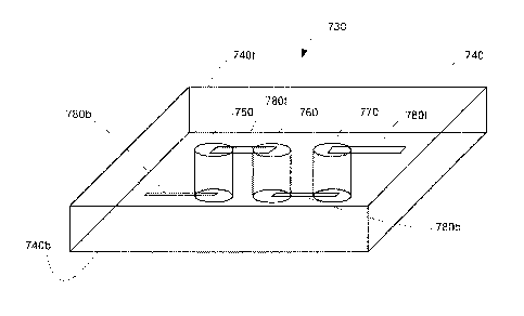
[0065] In Figure 18 a variable delay line 730 may be created by
connecting any
number of Z-directed delay line together by conductive traces on a PCB. These
surfaces are
to shown as transparent to illustrate the connections. Inserted in PCB 740
are cylinders 750,
760, and 770 which can represent either a Z-directed delay line, as
illustrated in Figures 17A
¨ 17C, or a conductive plug or Z-directed signal pass through component and
which are
connected in series fashion by top and bottom conductive traces 780t, 780b as
shown on the
top and bottom surfaces 740t, 740b of PCB 740. Cylinders 750, 760 and 770 may
also be
15 connected serially via conductive traces provided on internal layers of
PCB 740 if present or
by a combination of internal or external conductive traces. If cylinders 750,
760 and 770
each represent a Z-directed delay line element, then total delay across delay
line 730 may be
changed by replacing a Z-directed component delay line elements with a Z-
directed
component signal pass through device, previously described, that introduces no
significant
20 delay or with another Z-directed component delay line having a greater
delay. One
advantage of this configuration is that no changes are required to the PCB
layout design
while still allowing the total signal delay to be adjusted.
Z-directed T-Filter / PI Filter
[0066] A Z-directed T filter and a Z-directed Pi filter are three port
devices having an
25 input conductor, output conductor and a ground conductor. T filters are
generally comprised
of, for a low pass filter, two serial resistors connected between an input and
an output with a
capacitor connected between the resistors and to ground or, for a high pass
filter, two serial
capacitors connected between the input and an output and a resistor connected
between the
capacitors and to ground. Schematically these filters resemble the letter T.
Pi filters have
one component connected between input and output with a second component
connected
between input and ground and a third component connected between the output
and ground.
The first component may be a resistor and the second and third component may
be capacitors
CA 02823706 2013-07-03
WO 2012/099598
PCT/US2011/022012
26
and vice versa. Inductors may also be used. These devices may be mounted in a
Z-directed
component in a similar fashion as the transistor shown Figure 8 and 9.
Z-directed Ferrite Bead
[0067] Figures 19A ¨ 19C illustrate cross-sectional views of alternate
embodiments
of Z-directed ferrite beads. The construction of these devices is similar to
that shown and
described in Figures 5B ¨ 5H. Disposed, as shown in Figure 19A, in a portion
of the body
1000 is a cylinder 1001 of magnetic material having an opening through which
conductor
1002 passes. The conductor 1002 extends to the top and bottom surfaces of the
body 1000
where it is electrically connected to top and bottom traces. The conductor may
also be
to connected as previously described such as to a channel on the side
surface of the body or two
side channels etc. By varying the outside diameter cylinder 1001 the magnetic
properties are
varied controlling the characteristics of the ferrite bead. As shown cylinder
1001 is contained
within body 1000 but its outer circumference may also extend to the side
surface of body
1000. This construction creates a single conductor differential Z-directed
ferrite bead.
[0068] In Figure 19b two conductors 1002-1 and 1002-2 pass through two
openings
provided in cylinder 1001 in the body 1000 forming a two conductor
differential mode Z-
directed ferrite bead. The two parallel spaced apart conductors 1002-1 and
1002-2 are
enclosed by cylinder 1001 comprised of magnetic material. By varying the
outside diameter
cylinder 1001 the magnetic properties are varied controlling the
characteristics of the ferrite
bead. As shown cylinder 1001 is contained within body 1000 but its outer
circumference
may also extend to the side surface of body 1000.
[0069] Shown in Figure 19C, is a two conductor common mode Z-directed
ferrite
bead that is substantially similar to a two conductor differential mode Z-
directed ferrite bead
but with both of the conductors 1002-1, 1002-2 within the cylinder 1001a
passing through a
common opening 1003 in the magnetic material forming cylinder 1001a. The
volume within
opening 1003 is not filled with magnetic material. The volume may be left
empty, i.e. air
filled, or another nonmagnetic material may be used to filled the portion not
filled by
conductors 1002-1, 1002-2.
Z-directed Switch
[0070] The Z-directed component acting a single pole single position, or a
multi-pole
multi position switch may be used to program different settings into a PCB by
rotating it to
different positions about its axis of insertion. Figures 20A and 20B
illustrate a PCB 1101
CA 02823706 2013-07-03
WO 2012/099598
PCT/US2011/022012
27
having a multiplicity of internal layers 1102 having one or more conductive
traces and a
multiplicity of conductive surface traces 1103, three of which are further
designated as a, b
and c, on outer surface 1104. Conductive traces may be provided on both outer
surfaces of
PCB 1101. In Figure 20A, Z-directed component 1105 is mounted in mounting hole
1106
shown as a through hole. A channel 1107 of Z-directed component 1105 is shown
aligned
with circuit trace 1103a. The channel 1107 extends along the side surface 1105
from the top
surface 1105t to bottom surface 1105b. However the length of the channel may
be less the
length of the body of the Z-directed component and may extend only from one of
the top and
bottom surfaces toward the other or may be disposed intermediate the top and
bottom
to surfaces such as, for example, extending only between the two internal
layers of PCB.
Shown inserted into channel 1107 is a compressive conductive member, such as
rod 1109.
Provided in top surface 1105t of Z-directed component 1105 is turning
structure, such as slot
1108 used to rotate Z-directed component 1105 into alignment with the desired
surface trace
1103. Other configurations such as a pair of holes or cross-shaped slots may
also be used in
lieu of slot 1108.
[0071] Referring now to Figure 20B which is a sectional view taken
along line 20B-
20B of Figure 20A with Z-directed component 1105 removed, a multiplicity of
internal
connection points 1110 ¨ 1113 are shown. With compressive conductive member
1109 of Z-
directed component 1105 aligned with trace 1103a, connection between trace
1103a and
connection point 1110 is made as indicated by the dashed line interconnecting
these two
points. If compressive conductive member 1109 of Z-directed component 1105 is
aligned
with trace 1103b, then trace 1103b will be connected to connection point 1111
as indicated
by the dashed line interconnecting these two points. Similarly if compressive
conductive
member 1109 of Z-directed component 1105 is aligned with trace 1103c, then
trace 1103c
will be connected to connection points 1112 and 1113 as indicated by the
dashed line shown
interconnecting these three points.
[0072] When the compressive conductive member is a rod it may have a
diameter that
is less than and preferably equal to or greater than the diameter of channel
1107. In Figures
20C and 20D, compressive conductive rod 1109 is shown having a diameter that
is larger
than the diameter of channel 1107. This is done to ensure that compressive rod
1109 will be
compressed when inserted in channel 1107 helping to ensure that compressive
conductive rod
1109 will be retained within the body of Z-directed component 1105 due to the
interference
fit between the rod and channel. Further, as illustrated in Figure 20D,
channel 1107 is
CA 02823706 2013-09-09
28
positioned at the edge of Z-directed component 1105 so that the center line
1109a of
compressive conductive rod 1109 will positioned at a distance that is within
or less than the
radius R of Z-directed component 1105 while still allowing a strip 1109s of
the outer side
surface of compressive conductive rod 1109 to extend beyond the side
surface1105s of Z-
directed component 1105 to make the desired electrical connections. This strip
or portion
1109s of the outer periphery is exaggeratedly shown in Figure 20D. It is
expected that this
will also aid in keeping Z-directed component 1105 inserted into PCB 1101.
Additional
channels and compressive conductive rods may also be provided in Z-directed
component
1105 and arranged about the periphery of Z-directed component 1105 as needed
to meet the
design requirements for the circuit forming a multi-pole switch.
[0073] It will be realized that if diameter of compressive conductive
rod 1109 is equal
to or less than the diameter of the channel 1107 and the centerline of the
compressive
conductive rod is at or beyond the side surface of the body of Z-directed
component 1105, the
rod will tend to fall out of the channel. Some means such as an adhesive on
the portion of the
compressive conduct rod within the channel or on the surface of the channel
will need to be
used to retain the rod 1109 in channel 1107 when inserted therein prior to the
insertion of Z-
directed component 1105 into PCB 1104. With compressive rod 1109 having a
diameter that
is less than the diameter of channel 1107 shims or other means such as raised
portions in the
channel wall inserted between the channel surface and the compressive
conductive rod may
be used to ensure the compressive conductive rod will have a portion extending
beyond the
side surface 1105s of Z-directed component 1105.
[0074] In general, the channel shape and the compressive conductive
member shape
should correspond to one another so that the rod will be held by the channel
when it is
inserted therein while still allowing a portion of the compressive member to
extend beyond
the side wall of the Z-directed component. While cylindrical channels and rods
are described
it is understood that other shapes may also be used. For example, as shown in
Figure 20D,
channel 1120 is generally triangular or trapezoidal in section with the open
apex aligned with
the side surface. Shown inserted in channel 1120 is a generally rectangular
compressive
conductive member 1122 which has pinched-in waist 1122w caused by the
sectional shape of
channel 1120. Member 1122 may also have a triangular section as well.
[0075] Use of Z-directed component 1105 in this manner allows PCB 1101
to be
configured with an identification indicia such as a serial number using a
minimal number of
components. Connections between the surface layers of PCB 1101 (either top
surface,
CA 02823706 2013-07-03
WO 2012/099598
PCT/US2011/022012
29
bottom surface or both) can also be made to inner layers by the use of a well
provided in Z-
directed component 1105 as previously described. Further one or more wells and
one or
more center conductors may be used to provide for a multiplicity of
connections between and
among the internal layers 1102 and surface layers of PCB 1101. Although it is
contemplated
that once Z-directed component 1105 is positioned and aligned with the desired
traces it
would be plated in place, Z-directed component 1105 may also be removably
inserted into
mounting hole 1106 allowing for it to be realigned similar to a single-gang or
multi-gang
rotary switch, depending on the number of layers in PCB 1101. A slot may be
provided in
one of the end surfaces of Z-directed component to allow it to be rotated by a
screwdriver or
to other similar means. To hold Z-directed component in the mounting hole
while still allowing
for rotation, compliant strips or other similar means may be provided on the
circumferential
surface of the Z-directed component. When the mounting hole is a through hole,
the top
surface 1105t may have radial projections 1130 or a flange that can be used to
prevent the Z-
directed component from sliding out of the mounting hole when being rotated.
[0076] Building upon a Z-directed switch, the Z-directed component 1105 may
have a
number of different circuits or values of components, indicated by dashed
block 1115 in
Figures 20C, incorporated into the body thereof and be used to connect one or
more traces on
a layer of the PCB (interior or exterior layer) with another one of more
traces on the same or
other surfaces in the PCB using channels or conductors as previously
described. By having
multiple paths through a Z-directed component different circuits can be
selected by rotating
the part to select which conductor(s) is/are bridged that have the desired
circuit component
between 2 or more connection points. For example one Z-directed component may
have a
range of resistive values therein that are selected by inserting the Z-
directed component and
aligning it with the desired conductive traces. The concept may be expanded to
any
combination of electronic components that will fit within the volume of the
body of the Z-
directed component along with the necessary conductive traces.
Z-directed Internal Connector
[0077] One
of the problems with very high speed signals is that transitioning between
PCB layers requires a via hole to make the transition. The via copper has a
significant
surface area as compared to the signal. This causes a transmission line
discontinuity that may
affect the signal quality. Current high speed PCB designs sometimes require
these vias to be
back drilled to reduce the surface area of the via. An example would be when a
signal
transitions between two inner layers then the outer segments of the via may
need to be
CA 02823706 2013-09-09
removed. A drill bit is used to remove the copper between the surfaces of the
PCB down to
the area that the signal is located in the PCB. Figure 21A, 21C, and 21D
illustrate another
configuration of an internal Z-directed component connector that can make the
internal
connections without the need for this back drilling process. This embodiment
also illustrates
5 the use of test paths with the body of the Z-directed component. This
interior connector may
be used anytime a plating well is not desired to the top or bottom layers of a
PCB.
[0078] In this embodiment a Z-directed component 1200 has at least two
recessed
areas or pockets 1202a, 1202b, 1202c, 1202d on the side surface 1200s that
will contain a
solder paste material (not shown) that will either expand or reflow when
heated to make the
10 desired connections. A conductor 1216a, 1216b, 1216c, 1216d is provided
between top
surface 1200t and each of pockets 1202a ¨ 1202d, respectively. The portions
1216a1 ¨
1216d1 of conductors 1216a ¨ 1202d on surface 1200t may be used as test points
by test
probes as described herein.
[0079] Shown in the Figure 21B is a sectional view of a four-layer PCB
1210 having
15 two internal layers 1211a, 1211b, each having two conductive signal
traces 1212a and 1212b,
1212c and 1212d, respectively, provided at four internal locations in the wall
1214w of
mounting hole 1214. For purposes of illustration only, it is desired to
interconnect trace
1212a to trace 1212c and trace 1212b to trace 1212d. Other numbers of internal
layers and
signal traces may also be connected in a similar fashion using an
appropriately designed Z-
20 directed component internal connector. In Z-directed component 1200 four
correspondingly
positioned pockets 1202a - 1202d are positioned on side surface 1200s so that
when Z-
directed component 1200 is inserted into mounting hole 1214 these pockets will
be adjacent
to traces 1212a¨ 1212d respectively on internal layers 1211a, 1211b.
[0080] The pockets may be interconnected by a variety of means as is
known in the
25 art. Two examples are illustrated in Figures 21A and 21C. One is a
channel 1220 cut into
side surface 1200s interconnecting pockets 1202b and 1202d that may be filled
with solder
paste or into which the solder paste in the pockets will flow when heating of
the PCB occurs.
Additional channels interconnecting all of the pockets together can be
provided and the
pockets may be selectably interconnected by use of removable dams indicated by
dashed
30 lines 1224 provided in the channel 1220. This permits the
interconnections to be determined
after the Z-directed connector has been fabricated. Where a connection is
desired between
two pockets the dam 1224 in the channel interconnecting these pockets would be
removed.
The other connection may be done by a conductor 1222 provided in the body
1200b
CA 02823706 2013-07-03
WO 2012/099598
PCT/US2011/022012
31
interconnecting pockets 1202a and 1202c. With this arrangement the manner of
the
interconnection would need to be predetermined so that the conductors are
positioned
between the desired interconnection points.
[0081] Once the Z-directed component 1200 is soldered in place the
internal
connections can be checked by test probes placed on test points 1216a1 ¨
1216d1. For the
illustrated pairs of connections only a single test point is needed for each
pair of
interconnected pockets; however it may be desired to have a test point for
each connection
pocket as shown.
[0082] Figures 21C and 21D show Z-directed component internal connect
1200
to having an optional multi-terminal component 1230 either embedded or
formed within the
body 1200b. Component 1230 may be an active or passive component may also be
inserted
in the connection path to the internal layers 1211a, 1211b of PCB 1210. As
shown one
terminal of component 1230 is connected to top surface 1200t of Z-directed
component 1200
via conductor 1232, a second terminal is shown connected to pocket 1202a via
conductor
1234 and a third terminal of component 1230 is shown connected to pocket 1202d
via
conductor 1236. Components having more or less terminals may also be
accommodated
within Z-directed component 1200 depending on volume available for the
internal component
and conductors.
[0083] The test paths 1216a ¨ 1216d may not be present in some
designs. However,
the testing paths may be used with any of the Z-directed parts described
herein to improve
testability. Also the top and or bottom surface of this Z-directed component
may have a
conductive coating substantially coextensive with the surface to provide
further shielding
when the Z-directed component is installed and plated in a PCB.
[0084] In some cases depending on the desired function, a Z-directed
component may
work best when partially inserted into the PCB. A Z-directed component may
have a
parameter, such as resistivity that can be controlled by the depth that it is
inserted into the
PCB. One example would be a resistor that normally has a fixed resistive value
between the
top and bottom surfaces by applying a uniform resistive film over the side
surface of the body
This is illustrated in figures 22A and 22B illustrating a PCB 1300 having a Z-
directed resistor
1320 inserted at two different depths into a mounting hole 1302 indicated by
the dashed lines.
The PCB 1300 is illustrated as having signal traces 1303, 1305 on one external
surface, top
surface 1300t and signal traces 1307, 1309 on the other external surface,
bottom surface
CA 02823706 2013-07-03
WO 2012/099598
PCT/US2011/022012
32
1300b. As shown in both figures Z-directed resistor 1320 interconnects signal
trace 1303 to
signal trace 1305. Two internal layers are shown for PCB 1300, a first voltage
reference
layer Vcc 1311, and a second voltage reference layer GND 1313. Side surface
1330s of body
1330 has two closed end or blind channels, 1332, 1334 extending from top
surface 1330 t.
These blind channels could also both extend from the bottom surface 1330b. A
plateable
strip 1340 is shown disposed on side surface 1330s of body 1330 between the
top and bottom
surfaces 1330t, 1330b. Disposed within body 1330 are conductors 1335, 1336
electrically
connected to respective ends of plateable strip 1340. The other ends of
conductors 1335,
1336 are electrically connected to channels 1332, 1334. Line 1350 indicates
the position of
top surface 1300t with respect to body 1330. Z-directed resistor 1320 is
inserted into
mounting hole 1302 a depth D1 where portion P1 represent the portion of
plateable strip 1340
below the top surface 1300t of PCB 1300 and portion P2 represents the portion
of plateable
strip 1340 above. When the circuit board 1300 is plated the exposed side
surface 1300s
above the top surface 1300t along with portion P2 of plateable strip 1340
would be plated
with copper shorting out the portion P2 and reducing the overall resistance of
Z-directed
resistor 1320. The channels 1332, 1334 are closed ended to prevent the plating
material from
shorting the two channels together. In Figure 22B, Z-directed resistor is
shown inserted at a
greater depth D2. Accordingly on plateable strip 1340 portion P1 has increased
and portion
P2 has decreased. At insertion depth D2 and after plating has occurred, the
overall resistive
value of Z-directed resistor 1320 is greater than that when inserted at depth
D1.
[0085] This concept may be used with any passive element that can have
its value
adjusted by plating over part of a surface. One example is a Z-directed
inductor wherein
portions of the windings are exposed along the length of the side surface.
Another example is
a Z-directed capacitor having stacked disks similar to those as shown in
Figure 15 but
modified so as not to have the annular plate 617 connected to either of the
side channels 604,
608. Instead one or more of the annular plates 617 would be electrically
connected to a
corresponding conductor disposed within the body 605 with the other end of the
conductor
being exposed on the side surface of the body 605. A further example is a
signal delay line
such as that shown in Figure 17B having a portion of C-shaped conductors 705a
¨ 705d
exposed in the side surface 702bs. Another use for this partial insertion
technique would be
where different electronic functions exist in regions between the top and
bottom surfaces of
the body of the Z-directed component. As shown in Figures 7B multiple devices
or circuits
may be provided in the body 150. Internal connections may be provided to
plateable pads
CA 02823706 2013-07-03
WO 2012/099598
PCT/US2011/022012
33
provided in the side surface. The exposed pads would be shorted out by the
copper plating in
a similar way to the resistor example. As discussed later, a Z-directed
component can be
adjusted after the PCB has been manufactured. A circuit design may call for a
Z-directed
component providing an optional function or feature to the circuit to be
partially inserted into
the PCB and make no connections at the time of manufacturing. Later if the Z-
directed
component is needed to add its new function to the circuit in the PCB it would
be pushed into
place while in the field.
[0086] In another embodiment the strip used in a Z-directed variable
value
component may also have one or more etchable portions 1360 having a conductor
connected
to to each end of the strip (see Figure 22A). The conductors may be
internal to the body of the
component, provided on an external surface or be a combination of external and
internal
connects as previously shown and described. The value of the Z-directed
variable value
component would be adjusted by selectively etching away etchable portions 1360
of the strip
while still maintaining a signal path between the two end conductors. For
example, if the
strip were comprised of a resistive material, removal of some of this material
by etching
would decrease the value of the resistance. Depending on the material within
the etchable
portions the value of the component may increase or decrease as the material
is etched away.
Depending on the depth to which such a component is mounted in the PCB, fewer
or more of
the etchable portions would be exposed to etching.
Installation of Z-directed Components in a PCB
[0087] Given the shape and intended placement of a Z-directed
component to be
within a recess or through-hole in a PCB one way of achieving this placement
is by use of an
insertion system 800 comprising an orienting fixture 802 and ram plate 804 as
shown in
Figure 23. Positioned on orienting fixture 802 are one or more Z-directed
components 806.
Orienting fixture 802 using locating surfaces or other indicia provided on Z-
directed
components 806 ram plate orients these components for insertion into PCB 850
shown
positioned over orienting fixture 802 and having one or more mounting holes
852 for
receiving Z-directed component 806 therein as previously described. PCB 850 is
held by a
fixture not shown. As shown mounting holes 852 are through-holes and the depth
D of the
holes corresponds to the length L of Z-directed components 806. As previously
described the
length L may be less than, equal to or greater than depth D allowing for
recessed mounting,
flush mounting or extended mounting. For recessed Z-directed components,
resist material
CA 02823706 2013-07-03
WO 2012/099598
PCT/US2011/022012
34
will be needed to ensure that only those portions of the recessed surface that
are to be plated
will be plated and to avoid plating of the entire recessed surface.
[0088] Ram plate 804 is raised as indicated by arrow 860 inserting Z-
directed
components 806 into corresponding mounting holes 852 in PCB 850 through the
bottom
surface of PCB 850. The ram plate may have cylinders that press each component
806
through the orienting fixture 802 into mounting holes 852 to the correct
depth. These
cylinders may be individually operated or any combination at one time.
[0089] To facilitate use of a Z-directed component, insertion
equipment that
orientates the part and inserts them into the PCB will be needed. Although not
shown it
to should be realized that pick and place equipment may also be used to
insert a Z-directed
component into a PCB. Such pick and place equipment may insert a Z-directed
component
from either the top or bottom surface of a PCB. A plunger device will be
needed to press the
Z-directed component into the PCB to the desired insertion depth.
[0090] Z-directed components may be press fit or glued in place in a
PCB. The PCB
and Z-directed component interface can include resist material to prohibit
plating or seed
material to help facilitate plating. Examples are shown in Figures 24 and 25.
In Figure 24 a
Z-directed component 900 having a body 902 and two channels 904a and 904b
extending
along side surface 902s and a conductive top trace 906 is shown having a glue
strip 910 or a
glue dot 911on side surface 902s allowing Z-directed component 900 to adhere
to the wall of
a mounting hole in a PCB prior to plating. In Figure 25 a Z-directed component
920 having a
body 922 and two channels 924a and 924b extending along side surface 920s and
a
conductive top trace 926 is shown having copper seed material 927 indicated by
the
horizontal lines on channels 924a, 924b conductive trace 926 with resist
material 928
indicated by the angled lines on the remaining portions of side surface 902s.
Compliant
materials may be used to keep plating material from migrating past desired
locations. For
parts that extend past the surface of the PCB, the seed copper may be taken
around the edge
of a Z-directed component down the side surface to the surface of the PCB.
[0091] Other surface mount parts may be mounted over the part and may
even have
pads or balls to have surface mount parts connected directly to them. For
example, for ball
gate array devices, the balls may be attached directly to the top surface of a
Z-directed
component. Z-directed components may also be contained in a tape and reel
packaging
material. A part can be extracted using a pick and place vacuum head and be
partially
CA 02823706 2013-07-03
WO 2012/099598
PCT/US2011/022012
inserted in to a PCB. A camera can then be used to check the orientation of
the Z-directed
component and the Z-directed component position adjusted before being fully
inserted into
the PCB.
[0092] The foregoing description of several embodiments of the
invention has been
5 presented for purposes of illustration. It is not intended to be
exhaustive or to limit the
invention to the precise forms disclosed, and obviously many modifications and
variations
are possible in light of the above teaching. It is intended that the scope of
the invention be
defined by the claims appended hereto.
[0093] What is claimed: