Note : Les descriptions sont présentées dans la langue officielle dans laquelle elles ont été soumises.
CA 02823713 2013-07-03
WO 2012/094268 PCT/US2012/020006
1
METHOD AND APPARATUS FOR RESONANT CONVERTER CONTROL
BACKGROUND OF THE INVENTION
Field of the Invention
[0001] Embodiments of the present disclosure relate generally to power
conversion, and, in particular, to controlling power conversion in a resonant
converter.
Description of the Related Art
[0002] Resonant power converters consist of a bridge (full or half), a
resonant L-
C network (i.e., tank), and a rectification circuit. The bridge excites a
current in the
resonant tank which is rectified into a direct current (DC) output. The
rectification
acts as a resistive-like load which changes the quality factor (Q) of the
resonant
tank. By changing the frequency of the bridge voltage, the impedance of the
tank
network seen by the bridge changes, thus varying the tank current and output
power. Tank networks with high Q or networks with a "load independent point"
will
have large power swings over a relatively narrow frequency range, which can
make
it difficult for a controller to maintain stability.
[0003] Series resonant converters are designed to operate above resonance.
At
frequencies above the resonant frequency, the tank impedance looks inductive
to
the bridge and causes a tank current to lag behind the bridge voltage. When a
bridge device turns off, this lagging current can be used to charge/discharge
parasitic device capacitances to create zero-voltage switching. This is a well
known
technique for decreasing switching losses and allowing efficient operation of
the
converter at higher switching frequencies.
[0004] In traditional duty cycle controlled converters, one form of cycle-
by-cycle
control is accomplished through the control of peak current. Because the
current
waveform in traditional converters is always in phase with the switches, peak
current
control is a stable method of modulating power. Such a method is not suitable
for
resonant converters because the phase of the current with respect to the
switch
CA 02823713 2013-07-03
WO 2012/094268 PCT/US2012/020006
2
turn-off is unknown.
[0005] Therefore, there is a need in the art for a method and apparatus for
cycle-
by-cycle control of a resonant power converter.
SUMMARY OF THE INVENTION
[0006] Embodiments of the present invention generally relate to a method
and
apparatus for controlling resonant converter power production. In one
embodiment,
the method comprises determining accumulated charge processed by a resonant
converter; dynamically determining a level of the accumulated charge that
generates
a predetermined output power; and controlling a switching cycle of the
resonant
converter based on the level of the accumulated charge.
BRIEF DESCRIPTION OF THE DRAWINGS
[0007] So that the manner in which the above recited features of the
present
invention can be understood in detail, a more particular description of the
invention,
briefly summarized above, may be had by reference to embodiments, some of
which
are illustrated in the appended drawings. It is to be noted, however, that the
appended drawings illustrate only typical embodiments of this invention and
are
therefore not to be considered limiting of its scope, for the invention may
admit to
other equally effective embodiments.
[0008] Figure 1 is a block diagram of a resonant converter in accordance with
one or
more embodiments of the present invention;
[0009] Figure 2 is a block diagram of a controller in accordance with one or
more
embodiments of the present invention;
[0010] Figure 3 is a graph depicting primary side current and voltage for a
resonant
converter in accordance with one or more embodiments of the present invention;
[0011] Figure 4 is a set of graphs depicting a plurality of waveforms
associated with
the operation of the resonant converter in accordance with one or more
embodiments of the present invention; and
CA 02823713 2013-07-03
WO 2012/094268 PCT/US2012/020006
3
[0012] Figure 5 is a flow diagram of a method for cycle-by-cycle control of a
resonant
power converter in accordance with one or more embodiments of the present
invention.
DETAILED DESCRIPTION
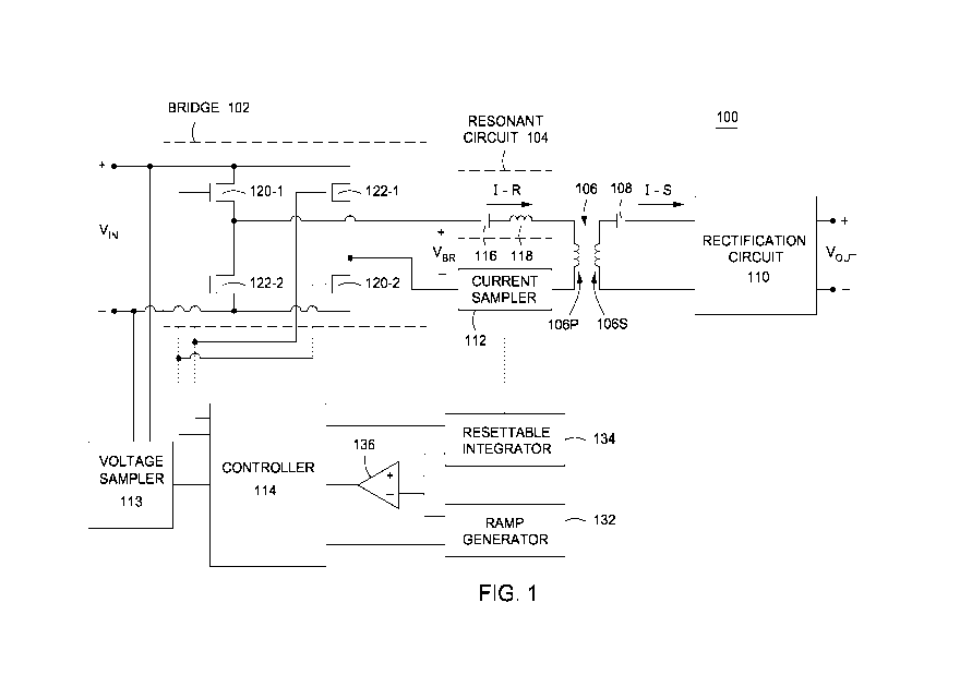
[0013] Figure 1 is a block diagram of a resonant converter 100 in
accordance
with one or more embodiments of the present invention. This diagram only
portrays
one variation of the myriad of possible system configurations. The present
invention
can function in a variety of power generation environments and systems.
[0014] The resonant converter 100 comprises an input bridge 102 ("bridge
102"),
a resonant circuit 104, a transformer 106, an output capacitor 108, a
rectification
circuit 110, a current sampler 112, a voltage sampler 113, a controller 114, a
ramp
generator 132, a resettable integrator 134, and a comparator 136. The bridge
102
comprises switches 120-1, 120-2, 122-1, and 122-2, arranged in an H-bridge
configuration such that switches 120-1/120-2 and 122-1/122-2 form first and
second
diagonals, respectively, of the H-bridge. Each of the switches 120-1, 120-2,
122-1,
and 122-2 is coupled to the controller 114 for operatively controlling the
switches.
The switches 120-1, 120-2, 122-1, and 122-2 may be any suitable electronic
switch,
such as insulated gate bipolar transistors (IGBTs), bipolar junction
transistors
(BJTs), metal¨oxide¨semiconductor field-effect transistors (MOSFET), gate
turnoff
thyristors (GT05), and the like. In some embodiments, the controller 114 may
be
coupled to both gate and source terminals of each of the switches 120-1, 120-
2,
122-1, and 122-2 for providing operative control. In other embodiments,
different
types of input bridge structures may be used for generating an appropriate
bridge
output voltage as described below.
[0015] A first output terminal of the bridge 102 is coupled between the
switches
120-1 and 122-2, and is also coupled to a first terminal of a capacitor 116. A
second
terminal of the capacitor 116 is coupled to a first terminal of an inductor
118, and a
second terminal of the inductor 118 is coupled to a first terminal of a
primary winding
106P of the transformer 106. The capacitor 116 and the inductor 118 form a
series
resonant circuit 104; in some alternative embodiments, other types of resonant
CA 02823713 2013-07-03
WO 2012/094268 PCT/US2012/020006
4
circuits (e.g., other types of series resonant circuits or parallel resonant
circuits) may
be utilized in place of the resonant circuit 104 within the resonant converter
100.
The current sampler 112 is coupled between a second terminal of the primary
winding 106P and a second output terminal of the bridge 102, which is coupled
between the switches 122-1 and 120-2. The current sampler 112 is further
coupled
to the resettable integrator 134. The voltage sampler 113 is coupled across
the
input to the bridge 102 and further to the controller 114.
[0016] On the
secondary side of the transformer 106, a first terminal of a
secondary winding 106S is coupled to a first terminal of the output capacitor
108.
The rectification circuit 110 is coupled between a second terminal of the
output
capacitor 108 and a second terminal of the secondary winding 106S. The
rectification circuit 110 may be any suitable circuit known in the art for
performing
rectification (e.g., a full wave rectifier or a half wave rectifier).
[0017] The
controller 114, in addition to being coupled to the switches 120-1,
120-2, 122-1, and 122-2, is coupled to the ramp generator 132, the resettable
integrator 134, and the comparator 136. The comparator 136 is also coupled to
the
ramp generator 132 and the resettable integrator 134.
[0018] The
bridge 102 receives an input voltage Vin from a DC voltage source,
such as one or more renewable energy sources (e.g., photovoltaic (PV) modules,
wind farms, hydroelectric systems, or the like), batteries, or any suitable
source of
DC power. The
controller 114 alternately activates/deactivates the H-bridge
diagonals (i.e., 180 out of phase) to generate a bridge output voltage Vbr
that is a
bipolar square wave having a duty cycle D. As a result of the voltage Vbr, a
sinusoidal current I-R flows through the resonant circuit 104 and the primary
winding
106P. The alternating current through the primary winding 106P induces an
alternating current I-S in the secondary winding 106S, which flows through the
rectification circuit 110 to generate a DC output voltage Vout, where
Vout=aVin and
a is proportional to the turns ratio between 106P and 106S.
CA 02823713 2013-07-03
WO 2012/094268 PCT/US2012/020006
[0019] The current sampler 112 samples the current I-R and generates values
indicative of the sampled current ("current samples"). In some embodiments,
the
current sampler 112 comprises an analog-to-digital converter (ADC) for
generating
the current samples in a digital format. The current sampler 112 couples the
current
samples to the resettable integrator 134 for integrating the current I-R over
time.
The voltage sampler 113 samples the input voltage Vin, generates values
indicative
of the sampled input voltage Vin ("input voltage samples"), and couples the
input
voltage samples to the controller 114. In some embodiments, the voltage
sampler
113 may comprise an ADC for generating the samples in a digital format
[0020] The resettable integrator 134 couples an output indicative of the
integrated current to a first input, e.g., a non-inverting input, of the
comparator 136.
The resettable integrator 134 receives an appropriate signal from the
controller 114
to reset the resettable integrator 134, for example during each switching
period.
[0021] The ramp generator 132 generates a ramp waveform with respect to
time,
i.e., a linearly increasing voltage, and couples an output signal indicative
of the ramp
waveform value to a second input, e.g., an inverting input, of the comparator
136.
The comparator 136 generates an output signal based upon the relative levels
of the
received integrated current and ramp waveform values. When the value of the
ramp
waveform exceeds the value of the integrated current, the comparator 136
generates a first output signal; when the value of the integrated current
becomes
equal to and exceeds the value of the ramp waveform, the comparator 136
generates a second output signal. The output from the comparator 136, which
indicates whether the integrated current or the ramp waveform is greater at a
given
time, is coupled to the controller 114.
[0022] In accordance with one or more embodiments of the present invention,
charge mode control is used to dynamically control cycle-by-cycle power
generation
from the converter 100, regardless of the phase of the current I-R through the
resonant circuit 104. During a first half of a switching period T, the
controller 114
activates the bridge 102 and monitors the accumulation of charge through the
resonant circuit 104 (i.e., the integrated current). Once the accumulated
charge
CA 02823713 2013-07-03
WO 2012/094268 PCT/US2012/020006
6
is sufficient to provide a desired output power Pout, the controller 114
deactivates
the bridge 102. As described in detail below with respect to Figure 3, the
accumulated charge is sufficient to produce the desired output power Pout when
it is
equal to (Pin*Ton))I(D*Vin), where Pin is the converter input power required
to
achieve the desired output power Pout (i.e., Pin is equal to the desired
output power
divided by the converter efficiency), Vin is the measured converter input
voltage, D
is the duty cycle for the bridge voltage waveform, and Ton is an "on" time for
the
bridge voltage waveform (i.e., an activation time for the bridge 102).
[0023] By modeling the instantaneous period (i.e., Ton) as a ramp waveform
via
the ramp generator 132, the slope of the generated ramp may be set as
PinI(D*Vin)
and the values of the ramp waveform and the integrated current may be compared
at the comparator 136 to determine when the charge accumulation is sufficient
to
produce the desired output power Pout. As the integrated current value
increases, it
eventually intersects and surpasses the ramp; at the point of intersection,
i.e., when
the corresponding values of the ramp waveform and the integrated current at a
particular time are equal, sufficient power has been put into the converter
100 for the
current switching half-period to achieve the desired output power Pout. As the
integrated current value increases, it eventually intersects and surpasses the
ramp,
causing the output from the comparator 136 to change and trigger the
controller 114
to deactivate the bridge 102 for the remainder of the switching half-period.
[0024] During the second half of the switching period T, the controller 114
may
activate the previously inactive bridge diagonal by any suitable technique to
generate an equal but opposite polarity bridge waveform. For example, in some
embodiments a simple mirror may be used (e.g., employing a timer) to drive the
bridge 102 during the latter half of the switching period T such that the
bridge
waveforms during the first and second switching period halves are equal but of
opposite polarity. In some other embodiments, the previously inactive bridge
diagonal may be activated during the second half of the switching period T
and,
analogous to the operation described above, the integrated resonant circuit
current
is compared to the generated ramp waveform to deactivate the bridge 102 when
the
CA 02823713 2013-07-03
WO 2012/094268 PCT/US2012/020006
7
two become equal. In such embodiments, the polarity of either the ramp
waveform
or the integrated current is reversed prior to the comparison; for example,
the
controller 114 may signal the resettable integrator 134 or the ramp generator
132 to
reverse the output polarity during the appropriate switching half-period. In
some
alternative embodiments, a second controller, analogous to the controller 114,
may
be used to drive the bridge 102 to generate the appropriate bridge voltage Vbr
during the second half of the switching period T.
[0025] In one particular embodiment, both the resettable integrator 134 and
the
ramp generator 132 are initialized at the beginning of a switching period T
and the
switches 120-1/120-2 are activated to produce a positive bridge voltage Vbr.
The
linear ramp waveform from the ramp generator 132 begins increasing positively
from
an initial value of zero and, as a result of the positive Vbr, the value of
the integrated
resonant current eventually increases positively at a rate greater than the
ramp
waveform. As the ramp waveform and the integrated current increase over time
they eventually intersect, thereby indicating that sufficient power has been
put into
the converter 100 for the current switching half-period. The point of
intersection may
be controlled by adjusting the slope of the ramp waveform; a steeper ramp
slope
results in a longer on-time for the switches 120-1/120-2 and a greater output
power
Pout. The output signal from the comparator 136 changes from one level to
another
as the value of the integrated current becomes equal to and begins to surpass
the
value of the ramp waveform, signaling the controller 114 to deactivate the
currently
active switch pair 120-1/120-2. The bridge 102 then remains inactive (i.e.,
Vbr is
equal to zero) for the remainder of the switching half-period as determined by
the
duty cycle D, which may be set in the controller 114.
[0026] In addition to controlling the operation of the bridge 102 based on
the
integrated resonant circuit current and the generated ramp waveform, the
controller
114 determines and adjusts the slope of the ramp waveform, for example during
each switching cycle, in order to dynamically achieve the cycle-by-cycle
control of
the power transferred to the output. As the ramp slope is increased, the
amount of
output power increases; as the ramp slope decreases, the amount of output
power
CA 02823713 2013-07-03
WO 2012/094268 PCT/US2012/020006
8
decreases. The ramp waveform slope may be adjusted to control each switching
cycle of the resonant converter 100 to achieve a desired output power Pout
based
on current operating parameters. For a known input voltage Vin, the slope of
the
ramp waveform may be determined based on a desired duty cycle D and a Pin that
will result in a desired output power level, as described below with respect
to Figure
3. The controller 114 is coupled to the ramp generator 132 and provides the
appropriate signals to the ramp generator 132 for adjusting the slope as
needed
during each switching cycle. In some alternative embodiments, the outputs from
the
ramp generator 132 and the resettable integrator 134 may be coupled to the
controller 114 and the controller 114 compares the integrated current to the
ramp.
[0027] Figure
2 is a block diagram of a controller 114 in accordance with one or
more embodiments of the present invention. The controller 114 comprises
support
circuits 204 and a memory 206, each coupled to a central processing unit (CPU)
202. The
CPU 202 may comprise one or more conventionally available
microprocessors or microcontrollers; alternatively, the CPU 202 may include
one or
more application specific integrated circuits (ASICs). The support circuits
204 are
well known circuits used to promote functionality of the CPU 202. Such
circuits
include, but are not limited to, a cache, power supplies, clock circuits,
buses,
input/output (I/O) circuits, and the like. The controller 114 may be
implemented
using a general purpose computer that, when executing particular software,
becomes a specific purpose computer for performing various embodiments of the
present invention.
[0028] The
memory 206 may comprise random access memory, read only
memory, removable disk memory, flash memory, and various combinations of these
types of memory. The memory 206 is sometimes referred to as main memory and
may, in part, be used as cache memory or buffer memory. The memory 206
generally stores the operating system (OS) 208 of the controller 114 that can
be
supported by the CPU capabilities.
[0029] The
memory 206 may store various forms of application software, such as
a converter control module 210 for controlling operation of the bridge 102
CA 02823713 2013-07-03
WO 2012/094268 PCT/US2012/020006
9
and performing functions related to the present invention, such as computing a
ramp
slope, setting a ramp slope in the ramp generator 132, activating/deactivating
the
bridge switches (e.g., based on signals received from the comparator 136),
resetting
the resettable integrator 134, initializing the ramp generator 132 (i.e., to
generate a
new ramp waveform from an initial value of zero), providing signals to the
resettable
integrator 134 and/or the ramp generator 132 for changing polarity of an
output, and
the like. The memory 206 may additionally store a database 212 for storing
data
related to the operation of the resonant converter 100 and/or the present
invention,
such as a duty cycle D, a desired output power Pout, a computed ramp slope, a
conversion efficiency e of the converter 100, and the like.
[0030] In other embodiments, the CPU 202 may be a microcontroller
comprising
internal memory for storing controller firmware that, when executed, provides
the
controller functionality described below.
[0031] Figure 3 is a graph 300 depicting primary side current and voltage
waveforms for a resonant converter 100 in accordance with one or more
embodiments of the present invention. The graph 300 can be utilized for
determining a formula for a slope of the ramp utilized in the switching
control of the
bridge 102.
[0032] The graph 300 comprises a bridge voltage waveform 302 depicting the
resonant converter bridge voltage Vbr over time, and a resonant circuit
current
waveform 304 (also referred to as "tank current waveform 304") depicting the
current
I-R through the resonant circuit 104 over time. The bridge voltage waveform
302 is
a bipolar square wave having a duty cycle D, and the tank current waveform 304
is a
substantially sinusoidal waveform phase-shifted with respect to the bridge
voltage
waveform 302.
[0033] At time TO, the switches 120-1/120-2 are activated while the
switches 122-
1/122-2 are inactive; the bridge voltage waveform 302 is at a positive value
and the
tank current waveform 304 is at a negative value increasing toward zero. At
time
T1, the bridge voltage waveform 302 remains at the positive value, and the
CA 02823713 2013-07-03
WO 2012/094268 PCT/US2012/020006
tank current waveform 304 crosses zero; a cross-hatched area Al depicts the
area
under the tank current waveform 304 from TO to TI. At time T2, the switch 120-
1 is
deactivated while the switch 120-2 remains activated and the switch 122-2 is
activated, effectively shorting the tank and resulting in a bridge voltage
waveform
302 of zero volts. The tank current waveform 304 is at a positive value, and a
cross-
hatched area A2 depicts the area under the tank current waveform 304 from T1
to
T2. At time T3, the switch 122-1 is activated, the switch 122-2 remains
activated,
the switch 120-1 remains inactive, the switch 120-2 is deactivated, and the
bridge
voltage waveform 302 drops to a negative value. The tank current waveform 304
is
at a positive value sinusoidally decreasing toward zero.
[0034] At time T4, the bridge voltage waveform 302 remains at the negative
value, and the tank current waveform 304 crosses zero; a cross-hatched area A3
depicts the area under the tank current waveform 304 from T3 to T4. At time
T5, the
switches 122-1/122-2 are deactivated and the bridge voltage waveform 302 rises
to
zero. The tank current waveform 304 is at a negative value, and a cross-
hatched
area A4 depicts the area under the tank current waveform 304 from T4 to T5. At
time T6, the switches 120-1/120-2 are activated while the switches 122-1/122-2
remain inactive; the bridge voltage waveform 302 rises to a positive value,
and the
tank current waveform 304 is at a negative value sinusoidally increasing
toward
zero.
[0035] The input power Pin to the resonant converter 100 can be expressed
based on the areas Al, A2, A3, and A4 as follows:
Vin*[(A2 + A4) ¨ (Al + A3)]
[0036] Pin= _________ T (1)
[0037] where Pin is an input power level that will result in a desired
output power
level Pout and [(A2-FA4)¨(A1-FA3)] is the accumulation of charge during the
switching period T. The relationship between the input power Pin and the
output
power Pout may be expressed as Pout = E * Pin, where E is a conversion
efficiency
of the resonant converter 100.
CA 02823713 2013-07-03
WO 2012/094268 PCT/US2012/020006
11
[0038] Since the resonant converter 100 is a full bridge converter
operating in
symmetric clamped mode, the bridge waveforms are running in symmetric mode
and the switches 120-1/120-2 and 122-1/122-2 are operating 1800 out of phase;
thus the area A2 is equivalent to the area A4, and the area Al is equivalent
to the
area A3. Further, the switch period T can be expressed in terms of an on time
Ton
for each diagonal and the duty cycle D, i.e., T=2* Ton/D, giving the equation:
Vin* D* [2(A2 ¨ Al)]
[0039] Pin = (2)
2 * Ton
[0040] Equation (2) can be rearranged as follows:
Pin* 2* Ton
[0041] = A 2 ¨ Al (3)
2* D*Vin
[0042] The difference between the areas A2 and Al is equivalent to the
integral
of the tank current waveform 304 from TO to T2:
Pin *2 * Ton
[0043] = j. Itank (4)
2* D* Vin
[0044] The on-time Ton can be approximated by a ramp function f-ramp that
models the instantaneous period:
Pin* framp
[0045] ¨ f /tank (5)
D*Vin
[0046] For a known (i.e., measured) input voltage Vin, a desired duty cycle
D,
and a required Pin to achieve a desired output power Pout, the ramp slope
Pin/D*Vin may be computed and utilized to achieve the desired output power
Pout
during a given switching cycle. In some embodiments, the controller 114 (e.g.,
the
converter control module 210) may compute a suitable value for the ramp slope
and
set the ramp slope in the ramp generator 132 based on the computed value. In
one
or more alternative embodiments, Equation (2) may be digitally implemented
(e.g., in
the converter control module 210) and the bridge 102 deactivated for a
switching
CA 02823713 2013-07-03
WO 2012/094268 PCT/US2012/020006
12
half-period when the desired Pin is reached.
[0047] Figure 4 is a set of graphs 400 depicting a plurality of waveforms
associated with the operation of the resonant converter 100 in accordance with
one
or more embodiments of the present invention. The set of graphs 400 comprises
a
graph 402, a graph 404, and a graph 406. The graph 402 comprises a bipolar
square waveform 408 depicting a voltage Vbr across the bridge 102 over time
("bridge voltage 408"). Graph 404 comprises a substantially sinusoidal
waveform
410 depicting a current I-R through the resonant circuit 104 over time ("tank
current
410"). Graph 406 comprises a waveform 412 depicting the integrated current I-R
over time ("integrated current 412") and a waveform 414 depicting the ramp
waveform over time ("ramp waveform 414").
[0048] At time TO, a first switching cycle begins and the switches 120-
1/120-2 are
activated while the switches 122-1/122-2 are inactive, generating a bridge
voltage
408 at a positive value. The tank current 410 is at a negative value that is
sinusoidally increasing toward zero. The integrated current 412 is zero and
begins
negatively increasing, and the ramp waveform 414 is zero and begins linearly
increasing with a slope as previously described with respect to Figure 3.
[0049] At time T1, the bridge voltage 408 remains steady. The tank current
410
crosses zero as it sinusoidally increases. The integrated current 412 is
negative
with a slope of zero as it begins to increase. The ramp waveform 414 is
positive and
continues to linearly increase.
[0050] At time T2, the bridge voltage 408 remains steady. The tank current
410
continues to sinusoidally increase. The integrated current 412 crosses zero
and
increases, while the ramp waveform 414 continues to linearly increase. At time
T3,
the integrated current 412 and the ramp waveform 414 are equal; the switch 120-
1
is deactivated while the switch 120-2 remains activated (although in other
embodiments both switches may be deactivated). The switch 122-2 is activated
once the bridge voltage 408 drops to zero (i.e., zero voltage switching). The
tank
current 410 is sinusoidally decreasing. The integrated current 412 and the
ramp
CA 02823713 2013-07-03
WO 2012/094268
PCT/US2012/020006
13
waveform 414 are reset to zero; in other embodiments, the integrated current
412
and/or the ramp waveform 414 may be reset to zero at a later time within the
current
switching period but prior to the beginning of the next switching period.
[0051] From T3 to T4, the bridge voltage 408, the integrated current 412,
and the
ramp waveform 414 remain at zero, while the tank current 410 continues
sinusoidally decreasing. At time T4, which is determined based on the duty
cycle D
being used, the switch 122-1 is activated, the switch 122-2 remains activated,
the
switch 120-1 remains inactive, and the switch 120-2 is deactivated, causing
the
bridge voltage 408 to drop to a negative value. The tank current 410 continues
sinusoidally decreasing, and the integrated current 412 and ramp waveform 414
remain at zero.
[0052] At time T5, the time from T4 to T5 being equal to the time from TO
to T3,
the switches 122-1/122-2 are deactivated and the bridge voltage 408 changes to
zero. The tank current 410 is negative and sinusoidally increasing. From T5 to
T6,
the time from T5 to T6 being equal to the time from T3 to T4, the bridge
voltage 408
is zero, the tank current 410 continues increasing, and both the integrated
current
412 and the ramp waveform 414 are equal to zero.
[0053] At time T6, a second switching cycle begins. The switches 120-1/120-
2
are activated and switches 122-1/122-2 remain deactivated to generate a
positive
bridge voltage 408. The tank current 410 is at a negative value that is
sinusoidally
increasing toward zero. The integrated current 412 is zero and begins
negatively
increasing, and the ramp waveform 414 is zero and begins linearly increasing.
Analogous to the operation during the time TO to T3, the switches 120-1/120-2
remain activated until the integrated current 412 and the ramp waveform 414
become equal at T7, at which time the switches 120-1/120-2 are deactivated.
The
slope of the ramp waveform 414 during the second switching cycle may be
different
from the slope of the ramp waveform 414 during the first switching cycle
(i.e., the
time from T6 to T7 may be less than or greater than the time from TO to T3)
based
on a desired change in output power during the second switching cycle.
CA 02823713 2013-07-03
WO 2012/094268 PCT/US2012/020006
14
[0054] Figure
5 is a flow diagram of a method 500 for dynamic cycle-by-cycle
control of a resonant power converter in accordance with one or more
embodiments
of the present invention. In some embodiments, such as the embodiment
described
below, the resonant converter is a full-bridge converter operating in a
symmetric
clamped mode (e.g., the resonant converter 100). The
resonant converter
comprises a resonant circuit, such as the series resonant circuit 104; in
other
embodiments, the resonant circuit may be another type of resonant circuit,
such as a
parallel resonant circuit. The resonant converter may further comprise a
resettable
integrator for integrating a current through the resonant circuit, a ramp
generator for
generating a linear ramp waveform, and a comparator for comparing the
integrated
current to the generated ramp (e.g., for comparing signals indicative of the
integrated current and ramp values), although in other embodiments other means
may be utilized for performing the functions with respect to the method 500.
[0055] The
method 500 begins at step 502 and proceeds to step 504. At step
504, converter operating parameters of desired output power, required input
power,
a desired switching waveform duty cycle, and input voltage are determined. The
required input power is the power to the resonant converter that will achieve
the
desired output power; i.e., the converter's efficiency e and the desired
output power
may be used to determine the required input power. The method 500 proceeds to
step 506, where a slope for the ramp waveform is computed. The ramp slope may
be determined as previously described with respect to Figure 3 based on the
required input power, the input voltage to the resonant converter, and the
desired
duty cycle for the switching period.
[0056] At
step 508, the slope of the ramp to be generated by the ramp generator
is set based on the computed value. The method 500 proceeds to step 510, where
a first switching cycle begins by activating a first diagonal of the resonant
converter's
input bridge to generate a bridge voltage of a first polarity, such as a
positive bridge
voltage. As a result of the bridge voltage, a substantially sinusoidal current
flows
through the resonant circuit on the primary side of the resonant converter.
The
resettable integrator begins integrating the current through the resonant
circuit (i.e.,
CA 02823713 2013-07-03
WO 2012/094268 PCT/US2012/020006
the resettable integrator determines the accumulated charge), and the ramp
generator begins generating the ramp waveform. The method 500 proceeds to step
512.
[0057] At step 512, the integrated current (i.e., the accumulated charge)
is
compared to the ramp waveform by comparing their corresponding values which
occur at a particular time. In some embodiments, values indicative of the
integrated
current and the ramp waveform are coupled to a comparator, such as comparator
136, for the comparison. At step 514, a determination is made whether the
values of
the integrated current and the ramp waveform are simultaneously equal. If, at
step
514, it is determined that the integrated current and the ramp waveform are
not
equal, the method 500 returns to step 512. If, at step 514, it is determined
that the
integrated current and the ramp waveform are equal, the method 500 proceeds to
step 516.
[0058] At step 516, the first diagonal is deactivated. As a result of both
bridge
diagonals being inactive, the bridge voltage drops to zero. In some
embodiments,
the integrator and the ramp are both reset (i.e., the values of each are reset
to zero);
in some alternative embodiments, the integrator and/or the ramp are reset at a
later
time during the switch period but prior to the next switch period. The method
500
proceeds to step 518, where the resonant converter input bridge remains
inactive for
a deadtime as determined by the selected duty cycle. The method 500 then
proceeds to step 520, where the second diagonal is activated to generate a
bridge
voltage of a second polarity, such as a negative bridge voltage. The second
diagonal remains activated for a time equivalent to the activation time of the
first
diagonal. As previously described above, the second diagonal may be activated
by
any suitable technique to generate a bridge waveform equal but opposite in
polarity
to the bridge waveform generated when the first diagonal was active. For
example,
in some embodiments a simple mirror may be used; in other embodiments, the
resonant circuit current may be integrated and compared to a generated ramp
waveform, where the polarity of either the ramp waveform or the integrated
current
is reversed prior to the comparison. The method 500 then proceeds to step 522
CA 02823713 2013-07-03
WO 2012/094268 PCT/US2012/020006
16
where the second diagonal is deactivated and the bridge remains inactive for a
deadtime, equivalent to the deadtime following deactivation of the first
diagonal, as
determined by the selected duty cycle.
[0059] The method 500 proceeds to step 524, where a determination is made
whether to continue operation of the resonant converter. If, at step 524, it
is
determined to continue operating the resonant converter, the method 500
returns to
step 504 to determine any operating parameter changes for the next switching
period and to adjust the ramp slope as necessary based on operating parameter
changes. The method 500 thus provides cycle-by-cycle control of the output
power
from the resonant converter.
[0060] If, at step 524, it is determined to discontinue operating the
resonant
converter, the method 500 proceeds to step 526 where it ends.
[0061] The foregoing description of embodiments of the invention comprises
a
number of elements, devices, circuits and/or assemblies that perform various
functions as described. These elements, devices, circuits, and/or assemblies
are
exemplary implementations of means for performing their respectively described
functions. For example, the integrator is an example of a means for
integrating a
current to determine accumulated charge processed by the resonant converter,
the
ramp generator is an example of a means for generating a ramp waveform, and
the
controller is an example of a means for controlling a switching cycle of the
resonant
converter based on a level of the accumulated charge that generates a
predetermined output power. Additionally, the comparator is an example of a
means
for comparing accumulated charge to a ramp waveform, and also for coupling a
signal to the controller based on a result of comparing the accumulated charge
to
the ramp waveform.
While the foregoing is directed to embodiments of the present invention, other
and
further embodiments of the invention may be devised without departing from the
basic scope thereof, and the scope thereof is determined by the claims that
follow.