Note : Les descriptions sont présentées dans la langue officielle dans laquelle elles ont été soumises.
CA 02824892 2013-07-16
WO 2012/098201
PCT/EP2012/050811
- 1 -
RESONANT POWER CONVERTER
The invention relates to a resonant power converter comprising a resonance
tank formed
by a capacitance component and an inductance component, at least two switches
con-
nected to the resonance tank and a voltage source in a bridge configuration, a
number of
snubber capacitors connected in parallel to each of the switches, and a
controller ad-
apted to control ON and OFF timings of the at least two switches so as to
excite the
resonance tank.
Power converters are used to transfer electrical energy from one circuit to
another. For
.. example, energy is transformed from the power grid to a load while
converting voltage
and current characteristics. Switching power converters are increasingly used
to replace
linear regulators and transformers because they offer high efficiency, small
size and
reduced weight.
A resonant converter of the type indicated above has been described by A.
Sokolow
"100-kW DC-DC Converter Employs Resonant-Filter", published on the Internet
site
http://powerelectronics.com in December 2010. Such converters are particularly
attrac-
tive for high power applications, i.e. for a power in the order of magnitude
of 10 - 100
kW.
Known resonant converters are typically operated at a fixed source voltage and
under
stable load conditions, so that it is possible to configure the converter such
that a Zero
Voltage Switching mode of operation (ZVS) is reached or at least approximated.
This
means that each switch should be switched to the ON state at a timing when the
voltage
drop across this switch crosses zero or at least reaches a minimum (valley
switching), so
that switching losses are reduced to minimum.
2
It is an object of the invention to provide a resonant converter that operates
with low
switching losses under varying operating conditions.
According to the invention, this object is achieved by resonant power
converter of the
type indicated above, wherein a voltage sensor is provided for sensing a
voltage drop
across at least one of the switches, and the controller is configured to
switch said at least
one of the switches to the ON state when the absolute value of the sensed
voltage drop
reaches a minimum.
Thus, when changes in the source voltage or changes of the load conditions
cause a shift
of the timings at which zero voltage switching or valley switching is to be
effected, the
converter according to the invention will automatically adapt to the changed
conditions.
More specific optional features of the invention are indicated herein. These
features
permit among others an efficient power conversion over a wide range of power
and
output current, an active power factor correction and a reduction of EMI.
In one embodiment, output current control is achieved by varying the switching
fre-
quency of the switches. In particular, the switching frequency is slightly
above the reso-
nance frequency of the resonant tank when the converter operates at full
power, and
when the switching frequency is increased further, the converted power and the
output
current will drop.
When the power demand decreases further, a continued increase of the switching
fre-
quency might result in increased switching losses and, correspondingly, a
reduced effi-
ciency of the converter. In these cases, it is possible to further reduce the
output current
by skipping some of the ON periods of the switches while keeping the resonance
tank in
resonance, or by operating the switches in a burst mode, where the periodic
pattern of
ON and OFF periods of the switches is chopped into a sequence of bursts
interrupted by
phases in which all switches are OFF.
CA 2824892 2018-04-17
CA 02824892 2013-07-16
WO 2012/098201
PCT/EP2012/050811
- 3 -
Next to controlling the output current, it is also possible to control the
input current, and
by employing nested feedback loops, it is also possible to control both, the
output cur-
rent and the input current. Control of the input current permits to maintain
an approxi-
mately sinusoidal input current curve and thereby to effect a power factor
correction.
Embodiments of the invention will now be described in conjunction with the
drawings,
wherein:
Fig. 1 is a
circuit diagram of a power converter according to a first
embodiment of the invention;
Fig. 2 shows wavefoi __________________________________ ins for
explaining the function of the power con-
verter shown in Fig. I;
Fig. 3 shows
waveforms illustrating a mode of operation with reduced
output current;
Fig. 4 is a
block diagram of a controller for controlling switches of the
converter shown in Fig. 1;
Figs. 5 and 6 show waveforms
illustrating different modes of operation of the
converter; and
Figs. 7 and 8 are
circuit diagrams of resonant converters according to modi-
fied embodiments of the invention.
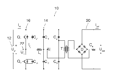
As is shown in Fig. 1, a resonant converter 10 is arranged to convert an input
voltage
Um into an output voltage U. The input voltage U,õ is a DC voltage or a
pulsating DC
voltage supplied by a voltage source 12.
CA 02824892 2013-07-16
WO 2012/098201
PCT/EP2012/050811
- 4 -
A resonant tank 14 is formed by an inductor Lr and two capacitor sets, one
capacitor set
being a parallel circuit of capacitors Cr, and Cr2, and the other set being a
parallel circuit
of capacitors C2 and C3 (LCC topology with parallel load). The resonant tank
14 is
connected to the voltage source 12 via a half bridge 16 formed by switches Qi
and Q2.
The switches Qi and Q2 are electronic switches, e.g. IGBTs. The gates of these
switches
are connected to an electronic controller 18 (Fig. 4) that will be described
later. A snub-
ber capacitor Cs1, Cs2 is connected in parallel to each of the switches Qi and
Q2.
The switches are alternatingly opened and closed at a switching frequency in
the order
of magnitude from 25 kHz to 50 kHz so as to cause the resonance tank 14, which
may
have a resonance frequency of 25 kHz, for example, to oscillate. The
capacitance com-
ponents of the resonance tank 14 are formed by the capacitors Cr' and Cr2
which are
arranged symmetrically with respect to the inductor Lr, just as the switches
Qi and Q2.
The capacitor Cri is connected between the plus pole of the voltage source 12
and the
inductor Lr, and the capacitor Ca is connected between the inductor L, and the
minus
pole of the voltage source.
The two capacitors C2 and C3 with equal capacity are connected in series
between the
plus and minus poles of the voltage source 12, in parallel with the resonance
tank 14.
When the resonance tank oscillates, a voltage Ur at the point connecting the
inductor L,
to the capacitors C2 and C3 will oscillate around a centre voltage that is
defined by the
mid-point between the capacitors C/ and C3. This voltage Ur drives the primary
side of
a transformer T the secondary side of which is connected to a rectifier 20
formed by a
diode full bridge D and capacitor C4. The voltage drop across the capacitor C4
forms the
output voltage U. When a load (not shown) is connected, a discharge circuit
for the
capacitor C4 is Closed, and an output current 'out may flow in this discharge
circuit.
When the switch Q1 is ON while the switch Q2 is OFF, an input current L will
flow
through the switch Qi and the inductor Lr to charge the capacitor Cr2. As long
as the
voltage drop across the inductor Lr is positive (Uin > Ur), a current Ir in
the resonance
CA 02824892 2013-07-16
WO 2012/098201
PCT/EP2012/050811
- 5 -
tank 14 will increase, and the capacitor Cri will be discharged. When
capacitor Cr has
been discharged completely, the inductor L, will cause the current I, to
continue, so that
capacitor Co will be charged further and capacitor Cri will be charged with
opposite
polarity. The voltage drop across inductor L, becomes negative and the current
I, de-
creases. Eventually, the current I, will change sign. Then, the switch Qi is
switched OFF
and switch Q2 is switched ON, so that the capacitors Cri and Ca will be
discharged via
the inductor Li- and the switch Q2. The current will increase until the
capacitor Ca is
discharged, and the current will gradually drop to zero while the voltage U,
becomes
negative relative to the minus pole of the voltage source 12. Then, the switch
Q2 will be
switched off and switch Qi will be switched ON again, so that another cycle
may start.
In this way, a primary current in the transformer T is kept oscillating, and
when the
switching frequency of the switches Q1 and Q2 is close to the resonance
frequency of
the resonance tank 14, a maximum of power will be transferred.
In order to prevent the voltage source 12 from being short-circuited via the
switches Qi
and Q2, the ON periods of these switches must always be separated by a certain
mini-
mum dead time. During these dead times, currents that would otherwise flow
through
the switches will be diverted into the snubber capacitors Co, Cs2 and, to a
smaller part,
into the device capacitances of the IGBTs.
Fig. 2(A) illustrates the sequence of ON and OFF periods of the switches Qi
and Q2. In
this example, the ON periods are separated by dead times Td which, for reasons
that will
become clear below, are larger than the minimum dead time mentioned above.
Fig. 2(B) illustrates a waveform of a voltage Us that is sensed by a voltage
sensor 22
(Fig. 1) at the junction point between the two switches Q1 and Q2. Thus, the
voltage Us
corresponds to the voltage drop across the switch Q2 whereas U1n - Us
represents the
.. voltage drop across the switch Qi. As a consequence of the symmetry of the
circuit
shown in Fig. 1, the waveform of the voltage Us shown in Fig 2(B) is point-
symmetric.
CA 02824892 2013-07-16
WO 2012/098201
PCT/EP2012/050811
- 6 -
Fig. 2(C) shows the voltage Ur of the resonance tank. In resonance, this
voltage is de-
layed by 90 relative to the voltage U.
Fig. 2(D) shows the current Jr in the resonance tank. This current is 90
ahead of the
voltage Ur and is thus at least approximately in phase with the (non-
sinusoidal) wave-
form of the voltage Us.
At the time t1 in Figs. 2(A)-(D), the switch Qi is ON, while the switch Q2 is
OFF. The
currentIr is supplied by the closed switch Qi, and the voltage Ur increases.
At the time
t2, the voltage Ur has reached its maximum and, accordingly, the current Ir
crosses zero.
At this instant, the switch Q1 is switched OFF. This zero current switching of
the switch
Q1 has the advantage that the detrimental effects of tail currents in the IGBT
switch Qi
are largely avoided.
The voltage U, which had been clamped to Uin is now allowed to drop, as shown
in Fig.
2(B). If the junction point between the switches Qi and Q2 were not connected
to the
resonance tank 14, the series connection of capacitors Cs1 and C52 would reach
an equi-
librium, and U, would drop to Uin/2. However, the snubber capacitors Cs1 and
Cs2 form
another oscillating circuit with the inductor Li., and this oscillating
circuit tends to dis-
charge C52 further. Ideally, U, would therefore drop to zero.
In order to reduce switching losses, the dead time Td should be selected such
that the
switch Q2 is switched ON in the very moment when Us reaches zero because,
then, no
energy that has been stored in the capacitor Cs2 would be dissipated when this
capacitor
is short-circuited. In practice, however, Us may not always reach exactly
zero, because
the oscillating circuit is subject to external influences such as fluctuations
of the input
voltage Uir, and changes of the load conditions. This is why the desirable
zero voltage
switching cannot always be achieved. What can be achieved, however, is a so-
called
valley switching, i.e. the switch Q2 is switched ON when Us (the absolute
value thereof)
reaches a minimum. The exact timing -(3 when this condition is fulfilled will
also depend
CA 02824892 2013-07-16
WO 2012/098201
PCT/EP2012/050811
- 7 -
upon the external influences mentioned above and may therefore vary for
varying oper-
ating conditions of the converter.
At the time t4, the switch Q2 will be switched OFF again (zero current
switching at
resonance), and the discharge process of the capacitor Cs, between t4 and t5
is the mirror
image of the process between t2 and t3. At t5, the switch Q1 is switched ON
again (valley
switching) and another cycle will start.
In the converter according to the invention, the controller 18 (Fig. 4) is
configured to
determine the ON switching timings t3 and t5 on the basis of the actual value
of the vol-
tage U, as measured by the voltage sensor 22, so that the ZVS condition or at
least the
valley switching condition can be fulfilled even under varying operating
conditions of
the converter.
In the example that is described here, the switching frequency of the switches
Qi and Q2
is varied in order to comply with varying demands for output current Tout. For
example,
the switching frequency may vary in an a range between 25 kHz and 50 kHz.
Fig. 3(A)-(C) show waveforms for a mode of operation in which the converter
operates
above resonance. Since the dead times Td are determined by the valley
switching condi-
tion, an increase of the switching frequency means that the duty cycle of the
ON periods
of the switches Qi and Q, becomes shorter, as has been shown in Fig. 3(B). The
switch-
ing frequency is determined by a clock signal CLK the waveform of which is
shown in
Fig. 3(A). The timings of the clock pulses correspond to the OFF switching
timings t2
and t4 in Fig. 2, i.e. the clock pulses alternatingly trigger the OFF
switching operations
of the switches Qi and Q2. The ON-switching operations will then be determined
by the
valley switching criterion.
Fig. 3(C) shows the voltage Ur of the resonance tank for the off-resonance
mode. Since
the switching frequency is higher than the resonance frequency, the phase
delay of the
CA 02824892 2013-07-16
WO 2012/098201
PCT/EP2012/050811
- a -
voltage Ur is larger than 90 , and the amplitude is smaller, so that less
power is trans-
ferred to the output side. The shortened duty cycles of the switches Ql and Q2
will also
contribute to the reduced power transfer (and also to a decrease of the input
current 'in).
The controller 18 will now be described in greater detail by reference to Fig.
4.
In this example, the voltage source 12 is formed by a power supply having a
diode full
bridge 12a for rectifying an AC grid voltage Ugrid. However, the power supply
does not
have a capacitor for smoothening the rectified voltage, so that the input
voltage Uli, for
the converter 10 has a waveform composed of sinusoidal positive half waves.
Further, it is assumed in this example that the converter 10 is current
controlled, i.e. the
output current 'our is controlled to a given target value designated by a
demand signal
'out setpoint that is supplied to the controller 18. The actual output current
Iout is measured
by a current sensor 24 and is delivered to the controller 18 as a feedback
signal.
A main unit 26 of the controller 18 compares the output current lout to the
demand signal
'out setpoint and generates a command signal Cmd that is supplied to a
multiplier 28. A
voltage sensor 30 detects the input voltage Uin and sends a signal
representing this input
voltage to another input of the multiplier 28. The product of the command
signal Cmd
and the input voltage Uin is supplied to a sub-unit 32 of the controller 18 as
a reference
signal Ijref. The sub-unit 32 compares this reference signal to the input
current Iill that is
detected by a current sensor 34. As a comparison result, the sub-unit 32
outputs a fre-
quency signal f to a clock generator 36. This clock generator further receives
a syn-
chronizing signal sync that is derived from the input voltage Uin and
generates the clock
signal CLK with the frequency f and synchronized with the pulsating input
voltage Uir,
and, indirectly, with the grid voltage Ugrid
The clock signal CLK is supplied to a switch controller 38 which further
receives the
voltage Us as sensed by the voltage sensor 22 and controls the gates of the
switches Q1
CA 02824892 2013-07-16
WO 2012/098201
PCT/EP2012/050811
- 9 -
and Q2. For example, the switch controller 38 may determine the ON-timings by
moni-
toring both, the absolute value and the time derivative of U. Thus, in a
normal mode of
operation, the switch controller 38 controls the OFF-timings of the switches
Qi and Q2
on the basis of the clock signal CLK and the ON timings of the switches on the
basis of
the sensed voltage U. The synchronisation of the clock signal CLK with the
grid vol-
tage has the advantage that undesirable interferences between the switching
frequency
and the grid frequency (50 Hz) are avoided and EMI is reduced
The frequency of the clock signal CLK is varied in order to control both, the
output cur-
rent 'out and the input current Iiõ. In an inner feedback loop comprising the
sub-unit 32,
the input current lin is controlled so as to preserve the sinusoidal waveform
of the input
current (power factor correction). The frequency of the clock signal CLK is
controlled
as to cause the input current lin to follow the reference value 'in ref which
is the product
of 15õ, and the constant (or slowly varying) command signal Cmd, so that Iiõ
is forced to
have the same sinusoidal half waves as Uin=
The amplitude of the half waves of Iiõ is determined by the command signal Cmd
which
is varied in an outer feedback loop comprising the main unit 26 and causing
the output
current Tont to follow the demand as specified by the demand signal lout
õtpoint=
The switch controller 38 has different modes of operation selectable by means
of a
mode signal Mod which the main unit 26 delivers to the switch controller 38.
For ex-
ample, since the clock signal CLK determines only the OFF timings of the
switches Qi
and Q2 and the ON timings are determined by the valley switching criterion, it
is clear
that a start mode should be provided for delivering the first or the first few
ON pulses to
the switches Qi and Q2 until the converter has started to resonate and a
meaningful vol-
tage Us can be derived. In a preferred embodiment, valley switching is only
allowed in a
pre-defined time window. If valley switching fails, outside the normal
operation condi-
tions, the switches are forced to switch on.
CA 02824892 2013-07-16
WO 2012/098201
PCT/EP2012/050811
- 10 -
When the demand represented by 'out sapoint decreases, the switching frequency
f may be
increased so as to reduce the output current Lull accordingly. However, when
the setpoint
is decreased further, a point will be reached where the switching frequency
must be so
high that even with the converter that is proposed here the residual switching
losses
would become predominant. This is why the switch controller 38 has additional
modes
of operation which permit to reduce the output current even beyond this point.
Fig. 5 illustrates, on a reduced time scale, the sequence of ON and OFF pulses
of the
switches Qi and Q2 for a mode of operation in which the power transfer is
reduced by
periodically skipping isolated ones of the ON pulses of both switches. In the
example
shown, one out of four ON-pulses of both switches is skipped, so that the
power transfer
will be reduced by 25%. The timings at which the ON-pulses of the two switches
are
skipped are offset relative to one another, which helps the resonance tank to
stay in the
resonant mode. Although random pulse skipping would be possible, it is
preferred to
use pre-defined regular pulse skipping patterns in order avoid random pulse
cancellation
and sub-harmonic output current variations.
Fig. 6 illustrates, on an even further reduced time scale, a mode of
operation, wherein
the sequence of ON pulses of both switches is chopped into bursts 40 that are
separated
by breaks 42. In practice, the number of pulses per burst will be
significantly larger than
shown in Fig. 6, large enough for the resonance tank to tune-in, and the
breaks 42 may
be so large that the resonance oscillations may decay until the next burst
begins. In this
way, the power transfer may be reduced to 50% or even less. Yet, given that
the switch-
ing frequency may be as high as 50 kHz, the repeat frequency of the bursts 40
may be
so large that the resulting ripple in the output current will be negligible.
Of course, it is also possible to combine the pulse skipping mode of Fig. 5
with the burst
mode of Fig. 6 in order to reduce the power transfer even further. Moreover it
is pos-
sible to vary the ratio between the skipped and the non-skipped pulses in the
pulse skip
mode and/or to vary the ratio between the length of the bursts and the length
of the
CA 02824892 2013-07-16
WO 2012/098201
PCT/EP2012/050811
- -
breaks in the burst mode, and all this may additionally be combined with
frequency con-
trol. For example, when switching from one mode to another, the converter
frequency
may be set to a pre-defined value, based on a frequency table or a suitable
algorithm, so
as to prevent a momentary step in the output current during the transition.
Fig. 7 shows a resonant converter 10' according to a modified embodiment. In
this em-
bodiment, the resonance tank has only a single capacitor Cr, so that the
circuit is less
symmetric than in the embodiment shown in Fig. 1. Nevertheless, the function
princi-
ples explained above can be applied. Further, the diode full bridge D that had
been
shown in Fig. 1 has been replaced by a half bridge of diodes D1, D2 and an
output in-
ductor Lf. The output capacitor C4 is connected to a centre tap of the
secondary winding
of the transformer T.
Fig. 8 shows another embodiment of a converter 10", wherein four switches Qi,
Q2, Q3
and Q4 form a full bridge, so that the converter can be powered directly by an
AC input
voltage Uin. In this full bridge configuration, the switches Qi and Q4 will
always be
switched simultaneously, just as the switches Q2 and Q. The resonance tank is
foitned
by the inductor Lr and a single capacitor Cr, and the voltage drop across the
capacitor Cr
is rectified by a diode full bridge D3 and a capacitor C4, so that a DC output
voltage is
applied to a load R.